

TEM A07A2200S Maintenance And Installation Manual
A07A2200S
TECHNICAL , MAINTENANCE
AND INSTALLATION MANUAL
2000 W FM TRANSMITTER
A07A2200S
380221

A07A2200S
ACCORDING TO R&TTE RULES
NOTIFIED BODY : 0523
All rights are strictly reserved
Reproduction or issue to third parties
in any form whatever
is not permitted without written authorization
380 221 R02 Pag. 2

Index
CHAPTER 1 : Safety Instructions pag.5
CHAPTER 2 : Electrical Specifications pag.7
CHAPTER 3 : General Description pag.10
CHAPTER 4 : Installation & Transmitter Setting pag.14
CHAPTER 5 : Circuit Description pag.30
CHAPTER 6 : Modulation Measurement pag.37
CHAPTER 7 : Remote Control pag.43
CHAPTER 8 : Internal Adjustment & Settings pag.50
CHAPTER 9 : Rear Connections & Settings pag.52
CHAPTER 10 : RF Amplifier Board pag.61
CHAPTER 11 : RF Filter pag.67

CHAPTER 12 : RF Detector
pag.68
CHAPTER 13 : Driver Exciter pag.70
CHAPTER 14 : Power Supply pag.71
CHAPTER 15 : Switch Front Pannel pag.76
CHAPTER 16 : AUDIO IN Board pag.77
CHAPTER 17 : DLCD Board pag.83
CHAPTER 18 : MBA Board pag.88
CHAPTER 19 : SINTD Board pag.95
CHAPTER 20 : DMPX Board pag.99
CHAPTER 21 : AGC Board pag.104
CHAPTER 22 : How to install GSM pag.108
CHAPTER 22 : How to use GSM pag.111
CHAPTER 23 : How to reach us pag.114

A07A2200S
SAFETY INSTRUCTIONS
1.1 Introduction
T.E.M. has always managed to improve the safety standard if its transmitting and receiving
equipment. All produced systems are tested in compliance with international EN60950 and
EN60215 rules.
Obviously this is not sufficient to avoid any accident during the installation and the use of our
equipment in compliance with EN60215 rule, the radio transmitters and the auxiliary equipment
must be used by qualified technical staff only and T.E.M.. declines any responsibility for damages
caused by an improper use or improper setting up performed by inexperienced staff, not qualified or
operating with instruments or tools not in compliance with safety set of rules.
WARNING
CURRENT AND VOLTAGE WORKING IN THIS EQUIPMENT ARE
DANGEROUS. THE STAFF MUST ALWAYS OBSERVE THE SAFETY
RULES, INSTRUCTIONS AND NORMS CONTAINED HEREIN.
WARNING
THE INSTRUCTIONS CONTAINED IN THIS MANUAL MUST BE READ
BEFORE SWITCHING ON OR SETTING THE TRANSMITTER
WARNING
ANY TRANSMITTER SERVICING, REPAIRING OR CHECKING
OPERATION REQUIRING THE OPENING OF THE TOP OR BOTTOM
COVER, MUST BE PERFORMED AFTER THE MAINS SUPPLY
DISCONNECTION WITHOUT REMOVING THE EARTH CONNECTION
WHICH THE EFFICIENCY MUST BE VERIFIED: THE CABLE MUST BE
IN GOOD CONDITIONS AND WELL CONNECTED.
WARNING
STAFF OPERATING UPON THE TRANSMITTER SYSTEM MUST NOT
BE TIRED: AFTER HEAVY WORKS OR CARRYING HEAVY
MACHINES BY HAND, IT IS NECESSARY TO RESPECT A PERIOD OF
REST BEFORE WORKING WITH SYSTEMS WHICH COULD HAVE
DANGEROUS ELECTRIC VOLTAGE IF THEY ARE NOT
DISCONNECTED.
380 221 R02 Pag. 5

A07A2200S
WARNING
SEVERAL SYMBOLS, INSIDE THE TYPICAL TRIANGLE SHOWING
DANGER, HAVE BEEN PRINTED ON SEVERAL TRANSMITTER
PARTS. ATTENTION SHOULD BE PAID, BECAUSE THERE COULD BE
THE DANGER DUE TO HOT SURFACES, ELECTRIC VOLTAGE
HIGHER THAN 50VOLT OR OTHER SPECIFIED DANGERS.
Certain devices (for example the RF final circuits mosfets) contain Beryllium Oxide BeO; these
components must not be broken, crashed or heated. This oxide passes through the common systems
of filtering, including the respiratory apparatus. The prolonged inhalation at high degrees causes
poisoning with respiratory apparatus paralysis, till death.
WARNING
ALL THE MODULES CONTAINING BeO ARE MARKED WITH THE
TRIANGULAR WARNING SYMBOL INDICATING THE NOTICE:
WARNING ! TOXIC HAZARD
THESE DEVICES CONTAIN BERYLLIUM OXIDE
OBSERVE SAFETY INSTRUCTIONS !
The staff in charge, besides being technically qualified, must have a practice of the first aid in case
of emergency or accident (reanimation, heart massage, mouth to mouth respiration, etc.).
Before going on with the operations to be performed, it is necessary to know the position of the
general electric switch and the one of the extinguishers, which are to be used very quickly if
necessary.
380 221 R02 Pag. 6

A07A2200S
A07A2200S FM BROADCASTING
TRANSMITTER
ELECTRICAL SPECIFICATION
2.1 FREQUENCY - POWER
Frequency range ------------------------------------------------------------------------------ 87.6 to 107.9MHz
Frequency setting ------------------------------------------------------------------------------------10 Khz steps
Internal setting mode -------------------------------------------------------------------------------------- by keys
External setting mode ---------------------------------------------------by remote control ( RS232-RS485 )
Frequency stability ----------------------------------------------------------------------------------±250Hz/year
Frequency generation ---------------------------------------------------------------------------PLL synthesizer
Modulation type------------------------------------------------------------ direct VCO frequency modulation
Nominal frequency deviation --------------------------------------------------------------------------- ±75KHz
Deviation linearity in all frequency range --------------------------------------------------------------±0.2dB
Peak detector error------------------------------------------------------------------------------------------<0.1dB
RF output power -------------------------------------------------------------------------------------- 0 to 2000W
Power resolution setting --------------------------------------------------------------------------------------- 1W
Power control limit setting ------------------------------------------------------------------------10 to 2000W
Power control stability ------------------------------------------------------------------------------------< 0.1dB
Reverse output power control limit ------------------------------------------------------------------1 to 200W
Reverse output power steps control-------------------------------------------------------------------------- 1W
Harmonics emission-------------------------------------------------------------------------------------- <-70dBc
Spurious emission ---------------------------------------------------------------------------------------- <-95dBc
Carrier reduction power ( carrier enable off ) --------------------------------------------------------- >70dBc
2.2 MODULATION CAPABILITY
MONO (left and right) -------------------------------------------------------------------------- 30Hz to 15KHz
STEREO (by internal stereo generator) ------------------------------------------------------ 30Hz to 53KHz
SCA (two channels) ----------------------------------------------------------------------------30Hz to 100KHz
COMPOSITE ----------------------------------------------------------------------MONO or STEREO + SCA
2.3 CHARACTERISTICS IN MONO
Signal input--------------------------------------------------------------------------------------------Left + Right
Input impedance --------------------------------------------------------------------- 600? (balanced) or 10k?
Unbalance rejection ----------------------------------------------------------------------------------------->40dB
Input level------------------------------------------------------------------------------------------- –6 to +12dBm
Pre-emphasis --------------------------------------------------------------------------------------------75 or 50? s
Audio frequency response (30Hz to 15KHz)--------------------------------------------------------- <0.15dB
Audio frequency response ( 19KHz to 100KHz) ------------------------------------------------------<-40dB
Modulation distortion ------------------------------------------------------------------------------------- <0.03%
Signal to noise ratio ----------------------------------------------------------------------------------------->85dB
380 221 R02 Pag. 7

A07A2200S
2.4 CHARACTERISTICS IN STEREO
Signal inputs------------------------------------------------------------------------------------------Left or Right
Input impedance --------------------------------------------------------------------- 600? (balanced) or 10k?
Unbalance rejection ----------------------------------------------------------------------------------------->40dB
Input level------------------------------------------------------------------------------------------- –6 to +12dBm
Pre-emphasis --------------------------------------------------------------------------------------------75 or 50? s
Audio frequency response (30Hz to 15KHz)--------------------------------------------------------- <0.15dB
Audio frequency response (19KHz to 100KHz) --------------------------------------------------------<40dB
Cross-talk between left and right channel --------------------------------------------------------------->50dB
Distortion at frequency deviation of 75KHz ---------------------------------------------------------- <0.03%
Distortion at frequency deviation of 100KHz --------------------------------------------------------- <0.03%
Signal to noise referred at deviation of 75KHz --------------------------------------------------------->80dB
Suppression of 38KHz -------------------------------------------------------------------------------------->70dB
Spurious suppression outside band -------------------------------------------.in according to ETS 300-384
Pilot reference for RDS encoder (19 Khz out) ----------------------------------------------------------- 1Vpp
2.5 SCA CHARACTERISTICS
Input (SCA1, SCA2) ---------------------------------------------------------------------------BNC unbalanced
Input impedance --------------------------------------------------------------------------------------------- 10K?
Frequency response (50KHz to 100KHz)---------------------------------------------------------------<0.1dB
Distortion -----------------------------------------------------------------------------------------------------<0.1%
Modulation capability------------------------------------------------------------------------------------0 to 10%
2.6 READOUT ON LCD DISPLAY (40x4 character )
Forward power resolution ------------------------------------------------------------------------------------10W
Reverse power resolution-------------------------------------------------------------------------------------- 1W
Modulation resolution----------------------------------------------------------------------------------------1KHz
Line voltage resolution ----------------------------------------------------------------------------------------- 1V
Power amplifier current resolution--------------------------------------------------------------------------0.5A
Heatsink temperature resolution------------------------------------------------------------------------------ 1°C
2.7 REMOTE CONTROL
COM1 (front panel) ---------------------------------------------------------------------------------------- RS232
COM2 (rear panel) ----------------------------------------------------------------------------------------- RS232
COM3 (rear panel) ----------------------------------------------------------------------------------------- RS485
Personal computer software ------------------------------------------- National Instruments LAB-VIEW ®
Transmission protocol ----------------------------------------------------------------------- AES-EBU SP 490
380 221 R02 Pag. 8

A07A2200S
2.8 POWER SUPPLY AND TEMPERATURE RANGE
Operating voltage---------------------------------------------------------------------------------230VAC ±15 %
Operating voltage(option)-----------------------------------------380VAC ±10 % Three phases + Neutral
Line power------------------------------------------------------------------------------------------------<3800VA
Nominal temperature range ----------------------------------------------------------------------- - -5° to 45°C
Operating temperature range---------------------------------------------------------------------- -10° to 50°C
Storage temperature range------------------------------------------------------------------------- -40° to 50°C
2.9 MECHANICAL SPECIFICATION
19” rackmount---------------------------------------------------------------------------------- 485x310x610mm
Weight---------------------------------------------------------------------------------------------------------- 47Kg
2.10 OPTIONS
Option A ------------------------------------------------------------------------------------------Stereo generator
Option B------------------------------------------------------------------------Automatic Audio Level Control
Option C------------------------------------------------------------------------------------------- Remote Control
2.11 STANDARDS COMPLYS ( R&TTE )
Electrical characteristics --------------------------------------------------------------------------- ETS 300-384
EMC characteristics -------------------------------------------------------------------------------- ETS 300-447
Safety characteristics---------------------------------------------------------------------EN-60950–EN-60215
380 221 R02 Pag. 9

A07A2200S
GENERAL DESCRIPTION
3.1 Main features
A07A2200S is a FM band broadcasting transmitter with modern conceiving and technology,
which by a simple design produces an output radio signal with high characteristics of quality,
reliability and security.
The simple manufacturing obtained with a hi integration of functions, has allowed to create
a machine with few controls and connections. Most printed circuits are multilayer with a surface
mounting technology component assembling. The eventual repairing can be done by simply
changing the fault involved board, without searching the defective component.
One of the most important characteristics is done by the high quality of the frequency
modulation and the high signal-to-noise ratio; moreover, the modulation is typically constant within
0.1dB throughout the whole FM band (88–108MHz ). A proper peak detector allows to perform
both traditional modulation measurements (usual bar-graph with peak), and modulation and power
modulation ones with long observation periods (even with many hours or days) according to the
latest international regulations, which properly cared to fix a limit scientifically measurable to the
peak and modulation power (CEPT 54-01).
An particular audio circuit can control the input audio level with a ±6dB dynamics referred
to the nominal value: this can be extremely useful when the audio signal level is not fixed or when
this one can be subject to fluctuations (usually very slow) due to thermal driftsbad systems
maintenance, possible damages along radio link paths etc. A proper board can be inserted to obtain
this function and a proper microprocessor follows constantly the modulation value correcting
through proper algorithms, implemented in its memory, the value of the modulator gain, keeping
this way the modulation very close to the maximum allowed value. The corrections take place at
very long periods of time; the board does not perform the audio compressing-limiting functions, but
just compensates possible drifts occurring on the systems carrying the audio channel before entering
in the FM transmitter. No measurable phase or amplitude distortion is introduced in the modulation
when the automatic gain control circuit is enabled. In addition an alarm which switches the power
off in case of modulation absence can be inserted since the unmodulated carrier transmission is
forbidden in many countries, with no chance to identify the radio.
The transmitter can be set like a modern signals generator so the output power is completely
managed by a device which guarantees that the values of forward power, reflected power,
maximum output power versus the temperature and loading conditions, are always the ones set or
the ones allowed by maximum limits. A directional wide band coupler with remarkable directivity
and large on board memory allows to obtain a power accuracy worthy of a good measurement
instrument.
All parameters (frequency, levels, mono/stereo, pre-emphasis, power) can be set by the
keyboard and stored in E
2
PROM in order to be kept even without electric supply. A great number of
events can be stored: each alarm is distinguished by a starting and an ending alarm date. The
controlled parameters are: modulation absence, heatsink temperature, mains supply voltage, RF
power final stage voltage and current, main oscillator fault.
380 221 R02 Pag. 10

A07A2200S
Besides the keyboard, the transmitter can be remotely controlled in different ways. A
personal computer can be connected as monitor to the DB9 socket placed on the front panel and by
a special program, to be load easily on the PC, all the transmitter parameters can be set and seen.
Furthermore it’s possible to perform all the modulation analysis provided by the CEPT 54-01
regulations and create the related graphics which can be stored as a file in the PC.
A second RS232 port placed in the transmitter rear part can be connected to the power
amplifier connected in series to the exciter, thus allowing the power data display on the same PC
connected to the front RS232.
A third RS485 port placed in the rear part can be connected to a MODEM which is
connected to the phone line thus assuring the transmitter telecontrol, remotely or from the studio.
The same RS485 port can be used for the connection N+1 of more transmitters (max 32). In
this case a transmitter acts as a “joker”, so it replaces the faulty equipment, automatically adapting
to all its parameters. Each transmitter is also provided with an output port (IN/OUT) suitable to
drive the antenna cable multiplexer and the one for the input audio signals switching.
3.2 Available options
a) STEREO ENCODER : additional board allowing the internal encoding of the
stereophonic signal
b) AGC : additional board allowing a frequency modulation
control
c1) REMOTE CONTROL : software for the PC connection
c2) N+1 system : software to obtain N+1 system
3.3 Block diagram
The transmitter can be modulated by five different audio signal.
The first two ones are made by monophonic left and right channels, which can be balanced
or unbalanced. The input dynamic goes from –6 to +12dBm with an input impedance which can be
high or low. On these channels either the European or American pre-emphasis value can be
inserted. A low pass filter on each of the two inputs assures a good attenuation of audio frequencies
higher than 15KHz which could interfere, in case of stereophonic transmission, with higher band
and with la subcarrier of the Multiplex signal; the out-of-band attenuation of the filter is not
excessive in order not to increase then phase distortion (group delay) of the in band audio signal:
60–70dB of attenuation, even with 0.1dB of amplitude linearity up to 15KHz, unavoidably creates a
distortion on the analogue signal that an experienced ear can perceive. Right or left signals can be
combined to generate monophonic transmission (should you only have one of the two signals, it
will be necessary to externally put in parallel the two inputs); in case of stereophonic transmission,
the two channels are fed inside the stereo code board.
380 221 R02 Pag. 11

A07A2200S
The mono signal or the stereo one, thus obtained, is combined with the other three possible
input audio signals: an external Multiplex signal and two SCA signals, one of which can be the
RDS one, which can be synchronized with a 19KHz one connected on the IN/OUT rear connector.
The composite signal can enter the AGC board, which has the task to check the its amplitude
and consequently to keep the modulation at the correct value, or it can follow its path and enter into
the frequency modulator after having passed through a limiter circuit (CLIPPER). This circuit must
became active just in cases of faults of previous circuits or in case of mistake in the setting of the
low frequency input nominal levels; this is to avoid to interfere with the adjacent channels. For not
activating this “fuse”, which produces remarkable distortions on the modulation, it is necessary to
take all proper cautions, that is the use of external compressor-limiters or by inserting the internal
AGC circuit which protects a lot against damages and drifts.
The oscillator, directly modulated by the composite signal, covers the whole FM band and
it’s synthesized in steps of 10KHz . The reference frequency is obtained by a 10MHz crystal kept at
constant temperature of 55°C, whilst the output frequency is set by the main microcontroller. The
oscillator phase noise is very good and it is in compliance with ETSI 300-384 regulations (<145dBc for a shifting of 1MHz from the carrier). The modulation linearity is typically contained
within 0.1dB without complicated corrections.
The RF final power circuit is wide band and it provides 2000W RF output controlled with
high accuracy; directional coupler has a directivity higher than 25dB on the whole band and an error
which is lower than 0.2dB, it is also compensated in temperature and totally shielded.
The power supply is of a switching type and it gives the four essential voltages, all obtained
with this technique. A small voltage measurement transformer allows to check the effective value of
mains supply voltage with accuracy and to interrupt the output power in case this value exits from
the normal operating window of the transmitter (10% respect the nominal value of 230VAC). The
mechanical position of the power supply and the final circuits of RF power allow to obtain a vent
flu just for cooling of the involved circuits, obtaining this way a really remarkable efficiency of that
function. In normal running conditions, when the transmitter is working in a full power at
environmental temperature, the radiator temperature is lower than 40°C, whereas the other circuits
temperature does not exceed 30°C. No components are involved with the air flow, in any case there
is a filter on the aspiration fan. The power supply is completely shielded both for internal circuits
and for its unavoidable emissions toward the outside.
Data displaying and setting is obtained by a board which is placed directly on the front panel
containing a microprocessor, memory, keyboard, LCD display. The displaying area is wide so
allowing to display and set needed data in a very easy way, thus making the transmitter-user
technician interaction extremely user friendly.
It’s possible to protect the transmitter input and output parameter settings with a password,
while all measurements can be done by whoever without interfering on its operation.
Two communication RS232 ports and a RS485 port can make possible the communication
between the transmitter and a PC, with the power amplifier and the driver exciter, or with a modem
connected with the telephone line.
Maintenance or repairing of damages do not require the soldering use for the replacement of
the parts to be changed; only six flat cables link all different boards.
380 221 R02 Pag. 12
A07A2200S
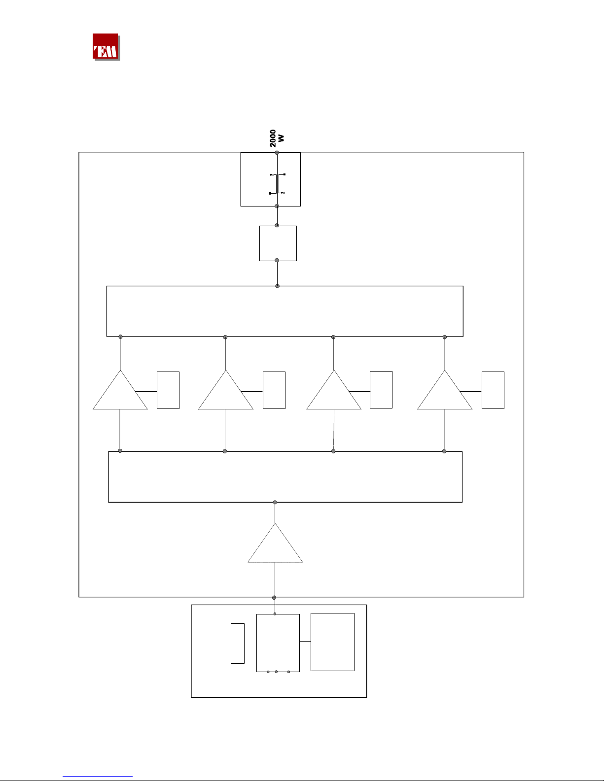
A07A2200S BLOCK DIAGRAM
380 221 R02
R.F. Wilkinson Divider.
Control Logic
Unit
R.F. Wilkinson Combiner
RF Exciter
Left
Right
MPX
R.F. Amp. 3
600 W
Forward
Reflected
RF
Output
R.F. Filter
Power Supply
R.F. Amp. 4
600 W
R.F. Amp. 2
600 W
R.F. Amp. 1
600 W
RF Amplifier Module
Pag. 13
48V 20A Power Supply
48V 20A Power Supply
48V 20A Power Supply
48V 20A Power Supply

A07A2200S
INSTALLATION
4.1 Unpacking and inspection
Immediately, after the transmitter has been delivered, please carefully check the package to
verify possible damages caused by shipment. Should be found some damages, please
immediately contact the T.E.M. dealer.
It is recommended to keep the original package for a future shipment due to, for instance, repairing
or setting. A return with a package which is different from the original one will make the warranty
rights lost.
4.2 Installation
The transmitter A07A2200S is composed of a 19 inches width rack which takes 7 units in height in
a vertical rack mount.
It is recommended to use 4 fixing plastic washers in order to avoid damages to the front panel
varnishing. We remind to carefully connect the earth both to the transmitter and to the rack mountnever disconnect it without having switched the supply voltage off by the mains switch.
Design has considered the new rules concerning the electromagnetic compatibility so there aren’t
problems to locate systems CE marked nearby.
4.3 Power supply
AC power supply at 50Hz can be at 230VAC single phase or option 380 V
AC
3 phases + neutral.
The switching on control (automatic type) is placed for security reasons on the rear panel with
exciter protection fuse, which must have the value 2 A for the higher voltage and 8 A (located on
the power supply modules, on the front) and it must be a delayed type.
BEFORE SWITCHING THE TRANSMITTER ON, MAKE SURE
THAT THE POWER SUPPLY IS CORRECT AND CONNECT
THE RIGHT LOAD OR ANTENNA!
380 221 R02 Pag. 14

A07A2200S
4.4 Ground loops
Sometimes connecting various ground sockets having different potentials may produce some
unwanted loops, which may create hum in the modulation: in this case it is essential to firstly
identify the origin of these currents, which normally spring from the antenna ground, mains
supply ground or from the input low frequency signals ground.
If the inconvenience can not be removed, the balanced input of the two channels LEFT and RIGHT
can be used, thus obtaining common mode noise rejection of 40dB approximately.
All the inputs and outputs are protected by diodes against the electrostatic discharges and they are
provided with filters against the RF noise.
4.5 Transmitter power up
After making sure about the proper earth socket connection, correct power supply and
connection of the load on the antenna output, the equipment can be switched on.
If there is the first switching on, problems of wrong setting can’t occur since the transmitter
contains some standard values and the output power will be set to 10W, in order to avoid any
problem of interference or driving for possible following amplifiers. The set values will be
displayed and changed according to your need before the RF power is emitted from the transmitter.
The equipment is provided with a memory which holds all settings even when the electric supply is
off, however it is recommended to set the power at 10 W when uninstalling the transmitter itself to
avoid any problem in case of a new setting up.
REMEMBER THE PASSWORD !
To enter the setting menu, knowing the password is mandatory. It’s a four digits number written on
the transmitter delivery document. Should it be forgotten, it will be possible to perform the set up
by setting the Z2 jumper placed on the board DLCD (vertical board placed behind the rear panel) on
the soldering side; the jumper is easy to identify through the close capture: PASSWORD ON/OFF.
In this case, this operation must be performed with the equipment switched off and it requires also
the opening of the top cover which, at ended operation, must be closed again with all its screws; it is
essential to use a proper cross point screwdriver.
4.6 Transmitter settings
4.6.1 At the switching on, the display will glow giving for few seconds the
following screen shot
380 221 R02 Pag. 15
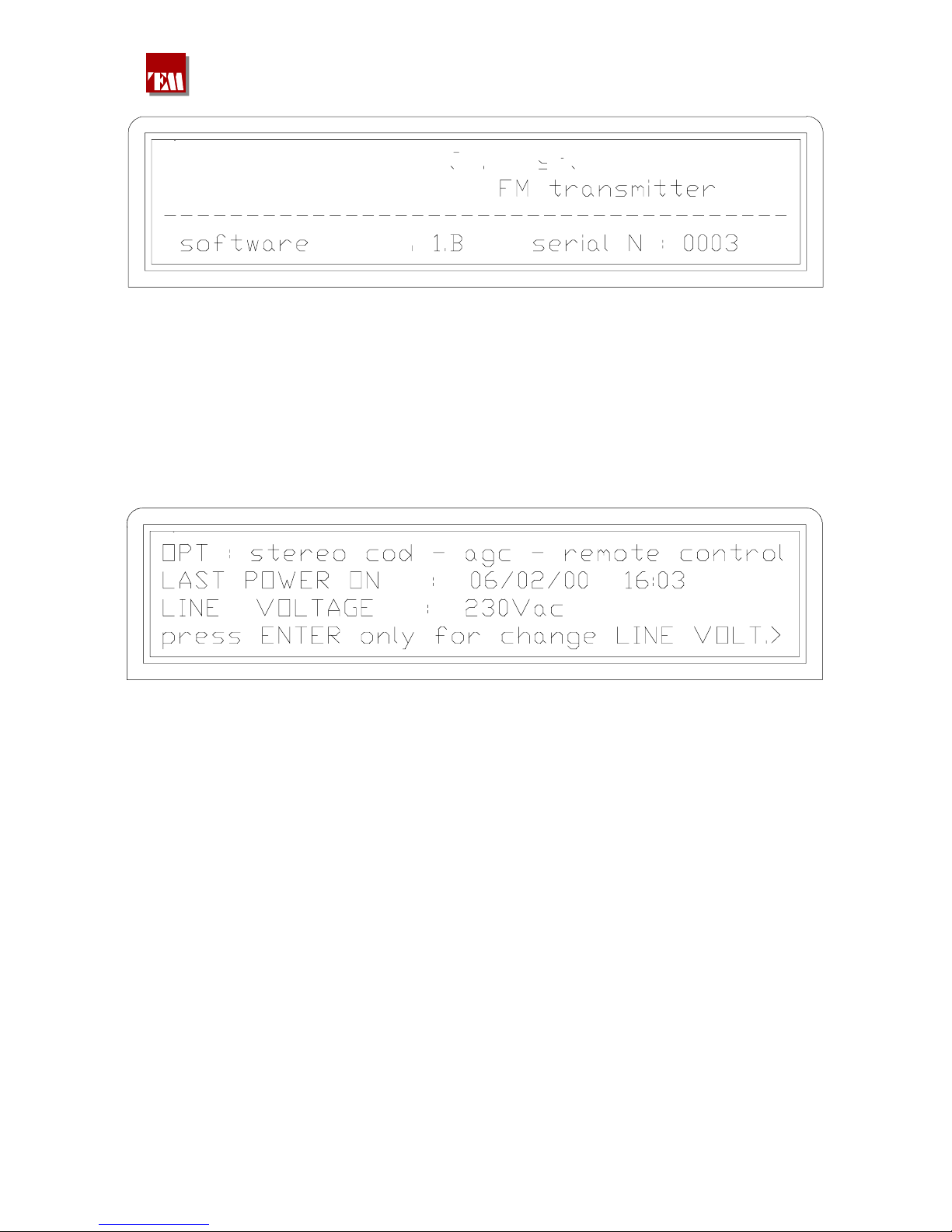
T.E.M
A07A2200S
T.E.M. S.p.A.
07A2200
T.E.M
4.6.2 Afterwards another page will appear for few seconds allowing to change the
mains supply voltage value; the value setting operation to 230VAC, allows the transmitter to operate
correctly, but it doesn't allow the microprocessor controlling the equipment to know the mains
supply voltage value. For this reason, if the value appearing on the said screen shot doesn't match
with the one set on the rear voltage changer, it will be necessary to type ENTER to update to the
changing; if the set value unmatched with the one read on the mains supply switch, the transmitter
will turn to MAINS SUPPLY VOLTAGE ALARM, for example reading a 220VAC voltage
If the line voltage appearing on the display matches with the one reading on the mains supply
switch, it isn’t necessary to type anything. On the opposite ENTER is required.
On the screenshot the options contained in the transmitter and the hour of the last switching on will
also appear and it will correspond to the current hour and date. If one finds out a discrepancy
between the hour given and the current one, it will be necessary to correct the error in the clock
setting.
If this screenshot is accessed from another menu, the indication LAST POWER ON will show the
last switching on date and it will be able to give the operator some indications about accidental
switching off.
4.6.3 If all the indications are right, after a while the first page will be shown;
which with the second one will contain all the most important measurements of the transmitter:
380 221 R02 Pag. 16
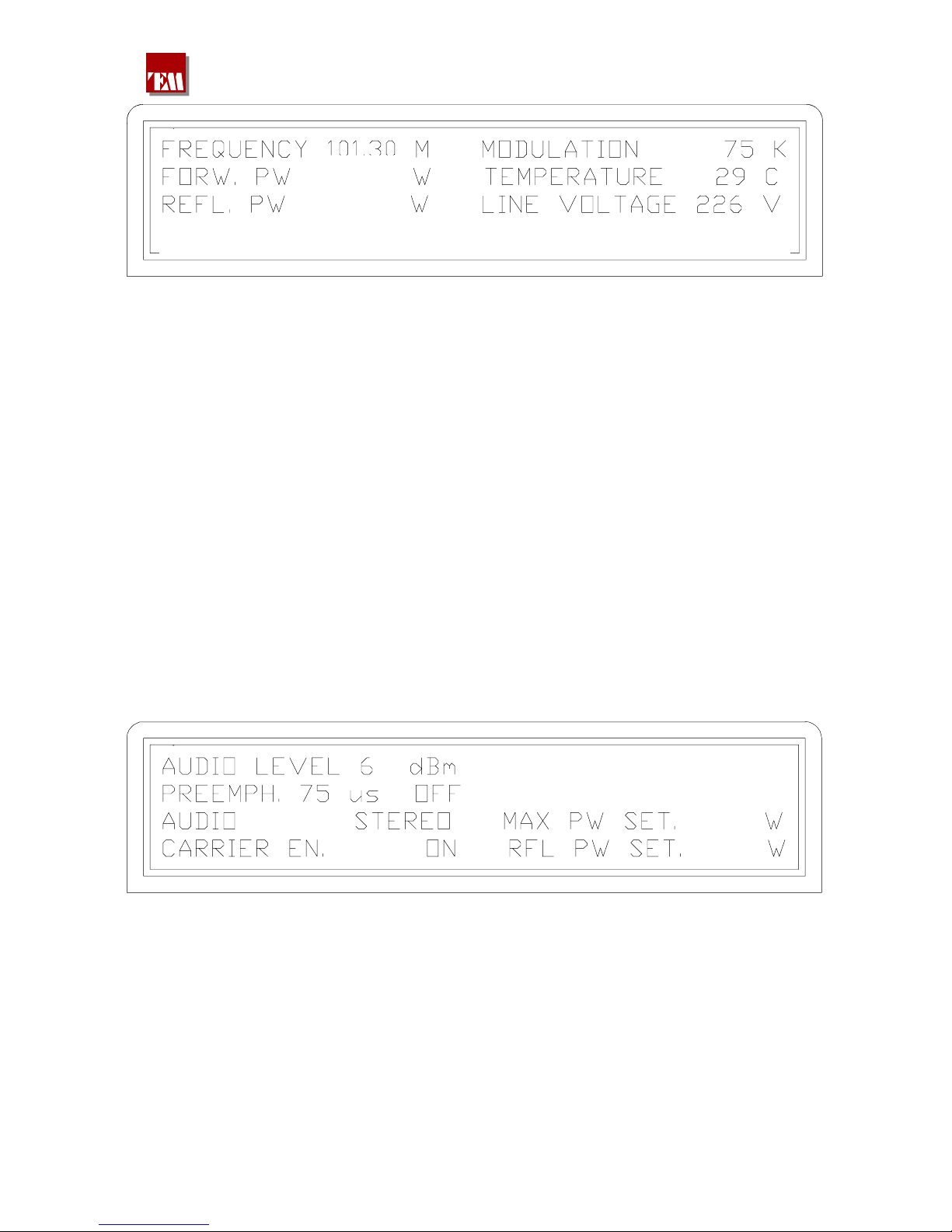
A07A2200S
2000
GSM > ON NO ALARMS I/O
-
> ON
32
The display is explanatory enough
FREQUENCY is the output frequency set in MHz
FORW. PW is the forward output RF power
REFL. PW is the input reflected power on the RF connector
MODULATION shows the modulation value of the COMPOSITE signal
TEMPERATURE shows the radiator temperature value of the RF power final mosfet
LINE VOLTAGE shows the mains supply voltage
Moreover, in the lower part of the display, at the middle there is the indication of the number of
alarms eventually set in the memory which have taken place after the last clearing of the memory.
These ones will be displayed automatically by a continuous enter of PAGE UP.
If one enters PAGE DOWN in this screen shot, the previous one returns and it will be possible to
see once again the date of the last switching on or to change the mains supplies voltages values.
If an alarm is on, always in the same position of the display, the intermitting message ALARM will
be pointed out.
4.6.4 By entering PAGE UP, it’s possible to see the second screen shot of the most
important measures:
PA V. 48,0 48,0 48,0 48,0
PA C. 17,3 17,3 17,3 17,3
2100
100
AUDIO LEVEL
PREEMPH. 75
AUDIO
is the nominal audio signal set on the setting window placed on the
rear panel: if this value doesn't match to the needed one, it’s possible
to choose 0 , 4.1 , 6dBm or, by placing the jumper on var, it’s
possible to choose a value between –6 and +12dBm.
is the chosen pre emphasis value, always on the rear window, also the
value 50µs can be selected; the inclusion or the disabling may be
performed by the keyboard in a following screen shot.
shows whether the transmitter is set to mono or stereo.
380 221 R02 Pag. 17
CARRIER EN
PA VOLTAGE
PA CURRENT
MAX PW SET
RFL PW SET
4.6.5
A07A2200S
shows if the output power is enabled either by a keyboard command
or by an external command through the IN/OUT rear connector.
is the supply voltage of the RF power final mosfet.
is the voltage drained by the mosfet final power.
is the maximum power value which can be programmed by the
keyboard in the screen shot Forward PW adj (10–2100W) to avoid
accidental over setting.
is the maximum allowed output reflected power. Should this limit be
reached, the direct power will be reduced to keep constant the limit
value of the reflected power
By entering again PAGE UP, eventual alarms present in the memory
will be displayed:
They are stored in a chronological order ordered by number, type and date.
Besides the real alarm, also the complementary event is stored (return to normality), in order to
know the alarm period time:
By entering PAGE UP, the next alarm is displayed, or, if in the last screen shot of main measures
there was not any alarm, it will be displayed the screen shot for the PASSWORD request to access
the measures. If inside the transmitter the Z2 jumper placed on the DLCD board (in the rear of the
front display panel board) is placed to OFF, this request is skipped, so it’s possible to directly set
the transmitter.
380 221 R02 Pag. 18
A07A2200S
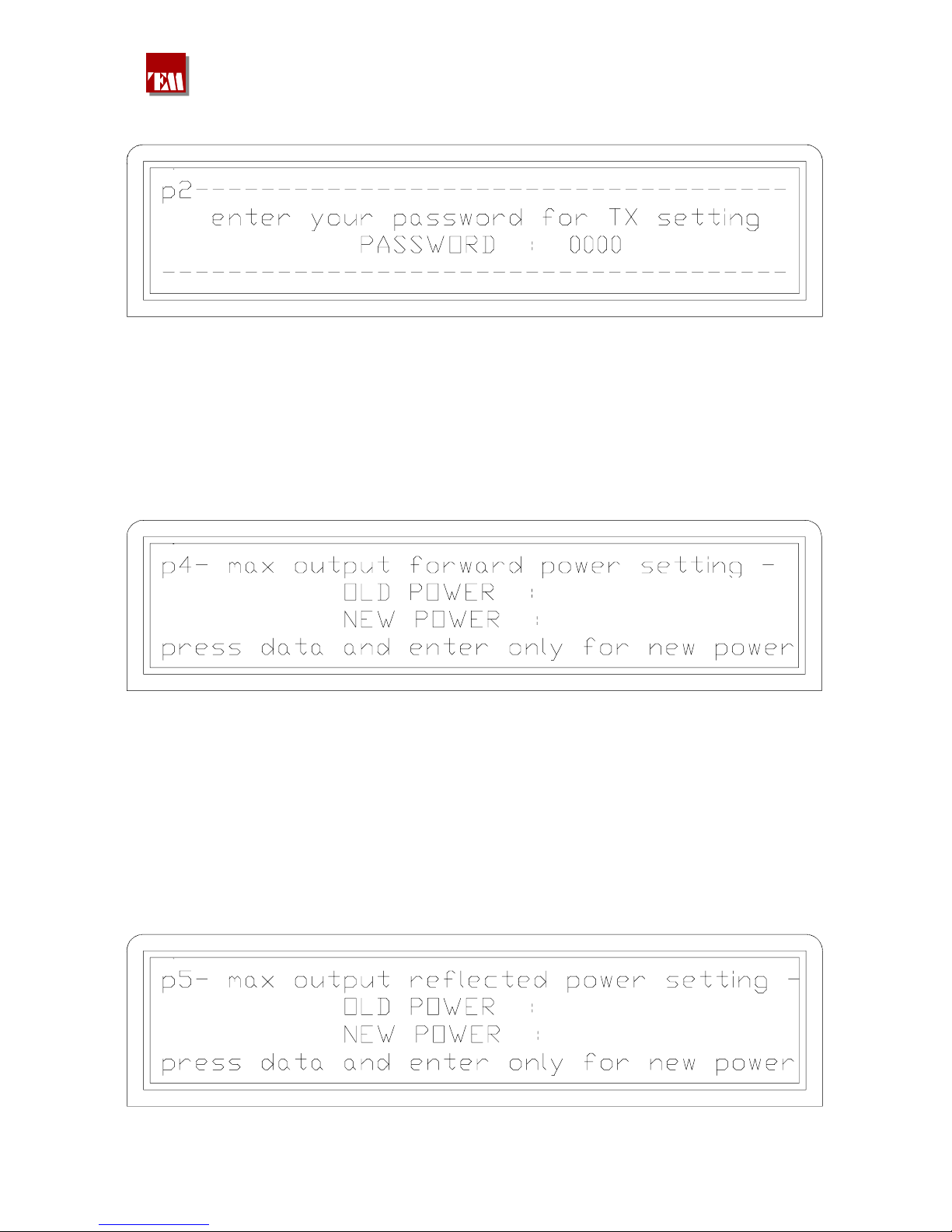
4.6.6 The screen shot for the password request is the following:
To go on, it is essential entering the four numbers which can be known by reading the transmitter
delivery document. If the password is unknown or it is too difficult to open the top cover by
unscrewing the 20 locking screws, it is just possible to surf among the previous screen shots which
give all the information about the transmitter.
4.6.7 By entering the right combination and then ENTER, the first setting of the
transmitter is accessed:
2000 Watt
1500 Watt
In this screen shot i the maximum value of the direct power setting can be changed by the keyboard
with the limit of 1500W; therefore in this screen shot output power can’t be adjusted, but a remedy
is taken to solve a quite common error in the output power adjustment of the exciter-amplifier
systems.
The change and entry of new data may be performed by pressing the horizontal and vertical cursors
and the ENTER button.
4.6.8 Entering instead PAGE UP, the following screen shot is accessed:
110 Watt
100 Watt
380 221 R02 Pag. 19

A07A2200S
In this screen shot, like in the previous one, it’s possible to set the higher limit of the allowed
maximum reflected power. If the set limit tends to be exceeded, for a bad antenna operation or a bad
load connected to the RF connector, the direct power is reduced proportionally so that this limit
won't be exceeded, thus protecting the RF power final mosfet. Usually the reflected power limit is
set to a value equal to 10% of the set direct power. Therefore, if the output power is adjusted at
1000W, the reflected one can be 100W.
The higher limit of this parameter is 99W and the resolution is 1W.
4.6.9 By entering PAGE UP, the following screen shot is accessed:
2000 W
2000 W
1 W
In this screen shot the output power can be set by means of NEW F. PW adj.. The resolution is
0.1W and the new direct power data are entered by the horizontal and vertical cursors and ENTER.
After the new power has been set, it will be possible to read the power measurement really present
on the antenna connector (forward and reflected), which may be slightly different from the set one
due to the control circuit error or it may be very different in case of standing waves on the output
circuit which forces the power control circuits to reduce the power in order not to exceed the
reflected power limits.
By means of the horizontal cursor, the power enable can be set, this software command doesn't
operate if the transmitter is externally disabled through a CARRIER EN control placed on the rear
IN / OUT connector.
On Factory request:
When there are not any alarms in the transmitter a +18V is present on pin 9 of In/Out rear
connector.
For externally disable the transmitter apply a signal in a range of +5V to +24
V on pin 8 of
In/Out rear connector.
These facility are normaly used when the transmitter is in the same system with a power
Amplifier in order to control the ON AIR process.
Each output power variation command is softly performed with the achievement of the final value
in 3 seconds approximately.
380 221 R02 Pag. 20
A07A2200S
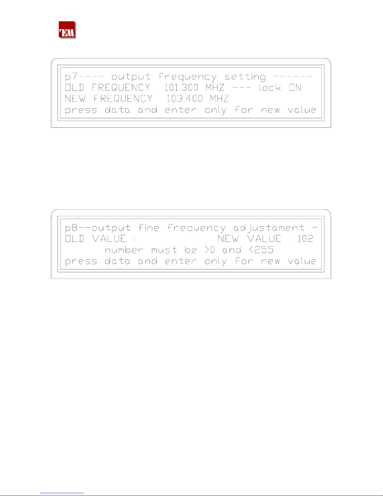
4.6.10 By entering PAGE UP the following screen shot is accessed :
In this screen shot the output frequency can be set by the usual cursors with a resolution of 10KHz.
On the display the current frequency and the new value appear.
After the ENTER key has been pressed for the new value, the output power is disabled for a few
seconds, allowing the oscillator to exactly reach the new value.
4.6.11 By entering PAGE UP, the following screen shot is accessed:
127
All the rules concerning the radio transmitters in FM band include some limits of accuracy and
stability of the output frequency. These limits usually depend on parameters of internal crystal
reference, which are at the same time connected firstly to the temperature and ageing of the crystal
itself. For this reason the crystal is heated at a constant temperature of 55°C, which guarantees a
considerable thermal stability, however a frequency correction due to ageing is easily implemented
just manually.
The present screen shot allows a very fine adjustment of the frequency value assigned to the radio
station without the need to open the transmitter. By entering a correction factor between 0 and 255,
the transmitter frequency can be corrected with a 20Hz step only; this operation can be performed
during the normal periodical check of the transmitter or, as it is shown below, through a remote
telecontrol.
By entering the new correction value, it’s possible to reach a 2KHz offset in comparison to the
central value.
380 221 R02 Pag. 21
A07A2200S
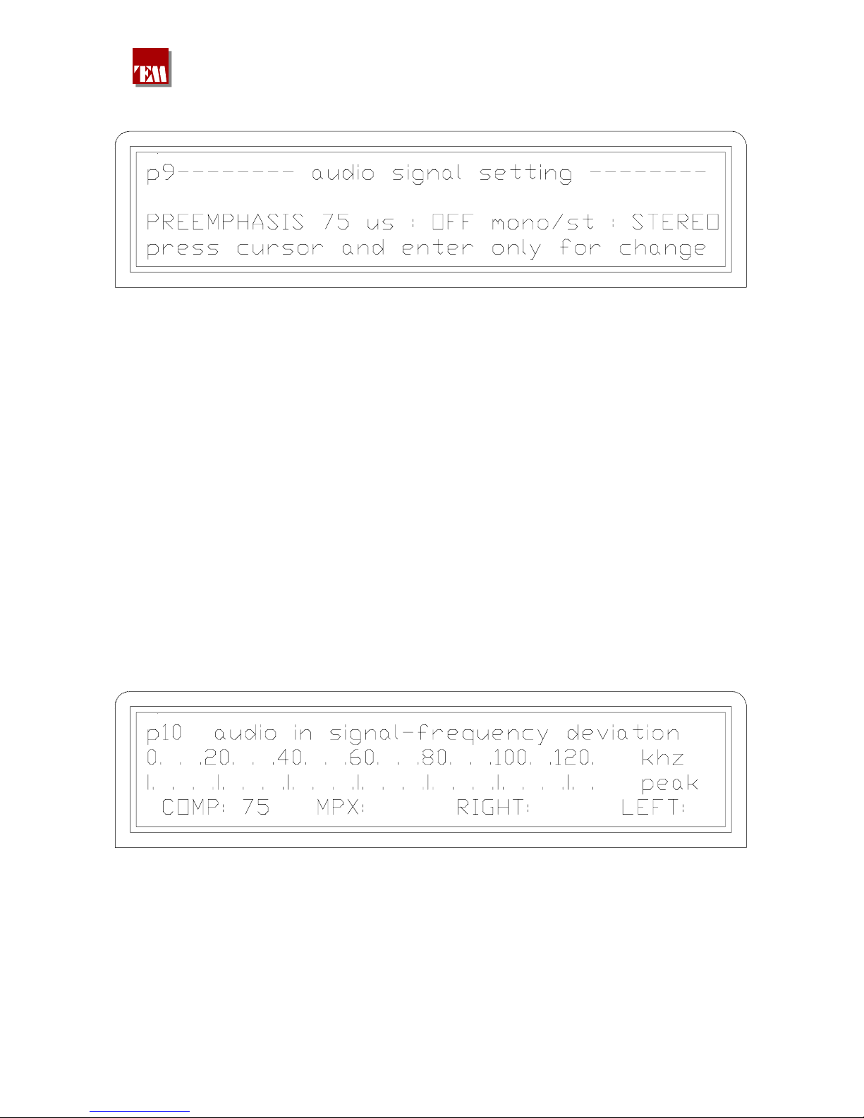
4.6.12 PAGE UP for a new screen shot :
In this case it’s possible to insert the pre-emphasis or to set the transmitter from mono to stereo and
vice versa.
The pre-emphasis value (50 or 75µs) is switched by a jumper placed on the rear window of the rack.
The pre-emphasis operates on the LEFT and RIGHT channels only.
By choosing the STEREO option, the LEFT and RIGHT channels are encoded with the stereo
subcarrier addition, from which it’s possible to get a synchronism in the IN/OUT rear connector
(1Vpp sine wave).
On the opposite, if an external stereophonic source is already available, the LEFT and RIGHT
inputs must be kept free by using the MPX input (rear BNC); in this case the transmitter must be
set to MONO even if the transmission is STEREOPHONIC.
When the transmission is monophonic, if one enters by the two LEFT and RIGHT channels, the
transmitter is modulated at the nominal value; if only one channel is available, this one must enter at
the same time both in the LEFT and RIGHT channel inputs, so they must be put in parallel
otherwise the deviation would be half of the nominal one.
4.6.13 By entering PAGE UP the following screen shot appears :
Here it’s possible to see the frequency deviation value and the input signal values.
When the composite signal is chosen (addition of all the modulating signals), the numerical and
visual indication appearing is the frequency modulation expressed in KHz while on the LEFT,
RIGHT MPX signals, the level is measured and displayed as value 100 when it matches the
nominal value.
The indication states the peak and the chosen measurement will be flashing displayed on the LCD.
380 221 R02 Pag. 22
A07A2200S
By modulating the transmitter through the nominal level input signals and with fixed tone (i.e..
400Hz), the deviation must not exceed 75KHz (COMP) and the input signal level must not exceed
100%. But if a music signal is available at the input, indication can also exceed this value and the
exact rules for this check will be seen in the screen shot 11.
Besides, if the automatic audio gain control is off, the 75KHz deviation value is equivalent to 100%
of the input signal values. On the opposite, if the AGC is on 75KHz deviation can be obtained by an
input signal which is variable, as level, from half to the double of the nominal value.
4.6.14 By entering PAGE UP the following screen shot will appear:
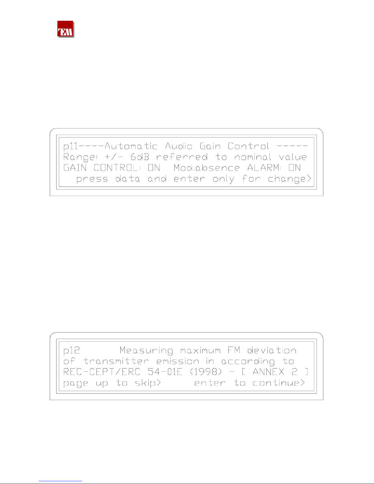
In this screen shot it’s possible to enter, if installed, the option of the modulation level automatic
control due to the audio signals: when the AGC is on, the maximum modulation value is checked at
75KHz varying the audio amplifiers gain; the dynamic is ±6dB and this is useful when the input
signal level is not sure.
For a wider explanation about the AGC operating see paragraph 4.4.
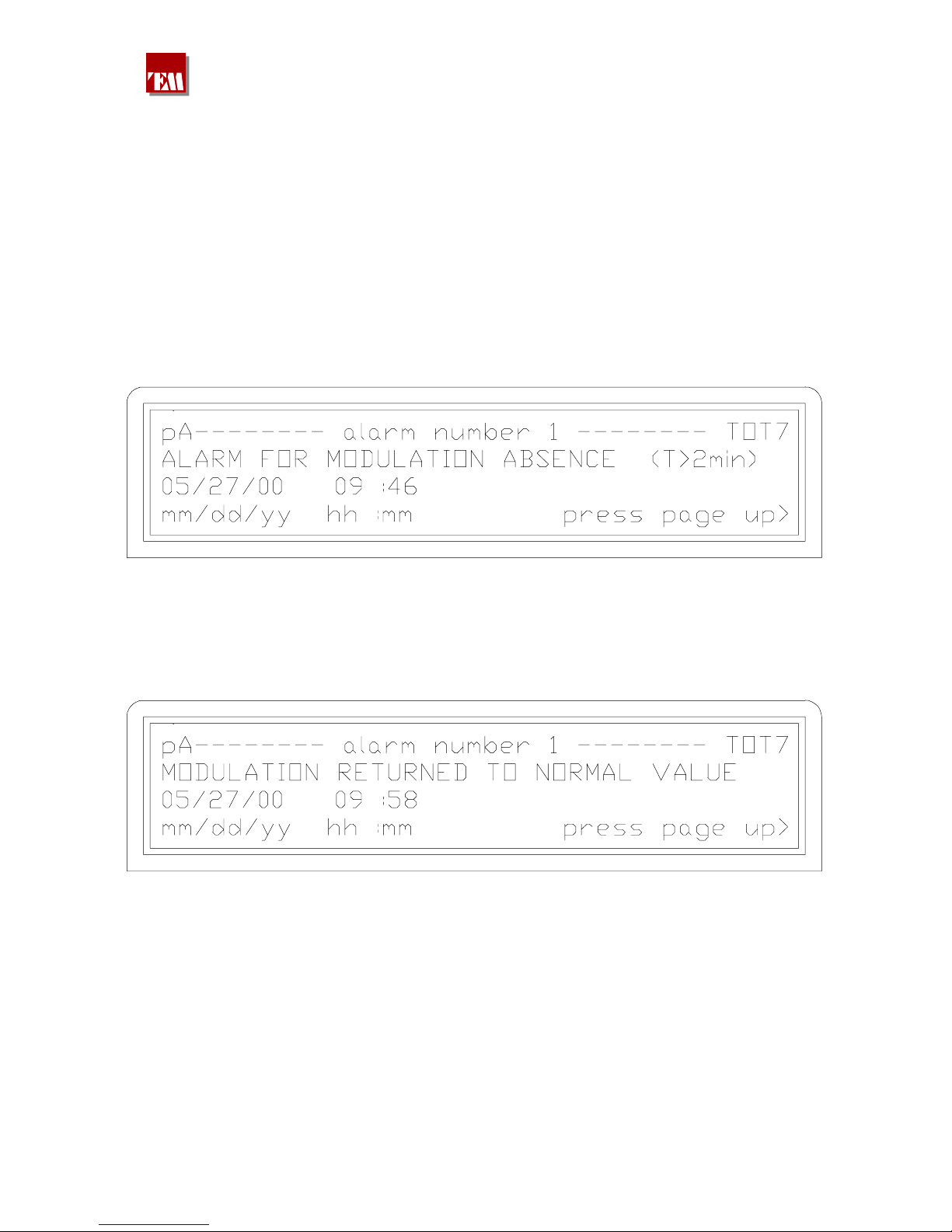
There is also a control on the modulation presence, since everywhere it isn’t allowed to transmit by
unmodulated carrier; after two minutes of modulation absence an alarm can be given and the power
can be disabled. When the modulation returns to the normal value, the alarm stops and the usual
operation is restored; in case of stereophonic transmission, the threshold for the modulation absence
is 10KHz, because of the subcarrier value.
4.6.15 By entering PAGE UP the following screen shot appear :
380 221 R02 Pag. 23
A07A2200S
380 221 R02 Pag. 24
A07A2200S
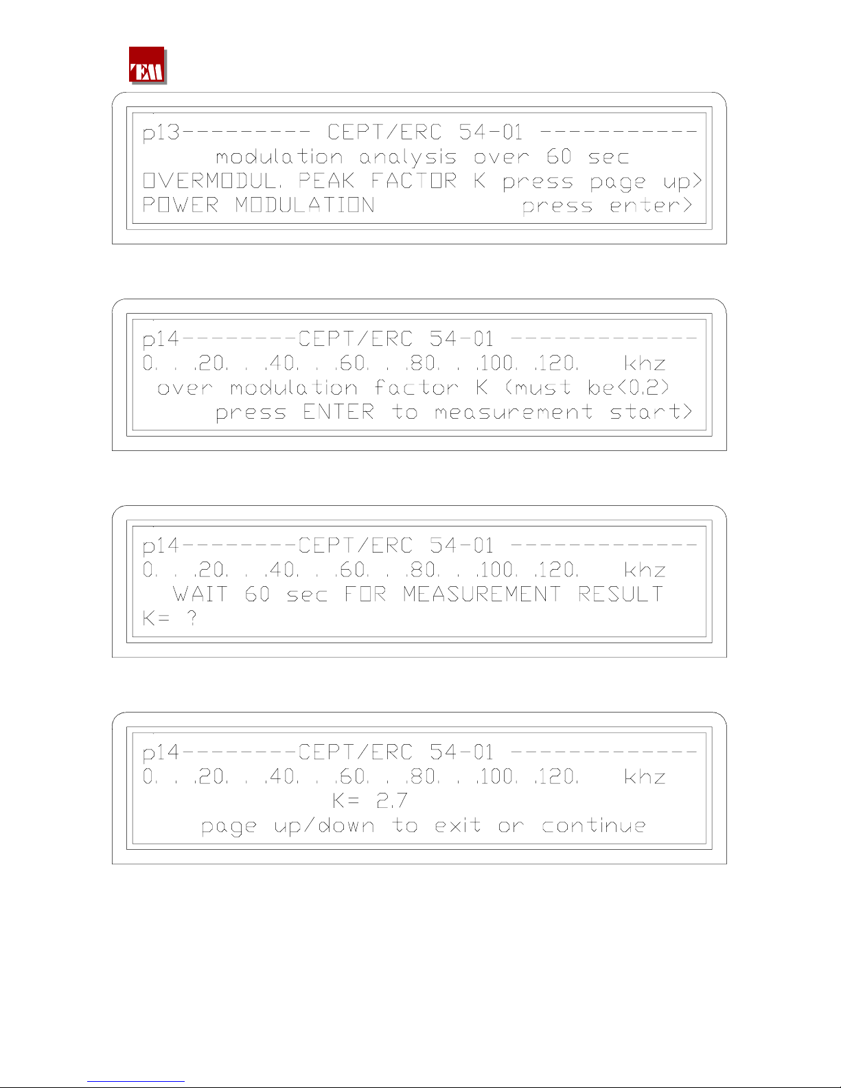
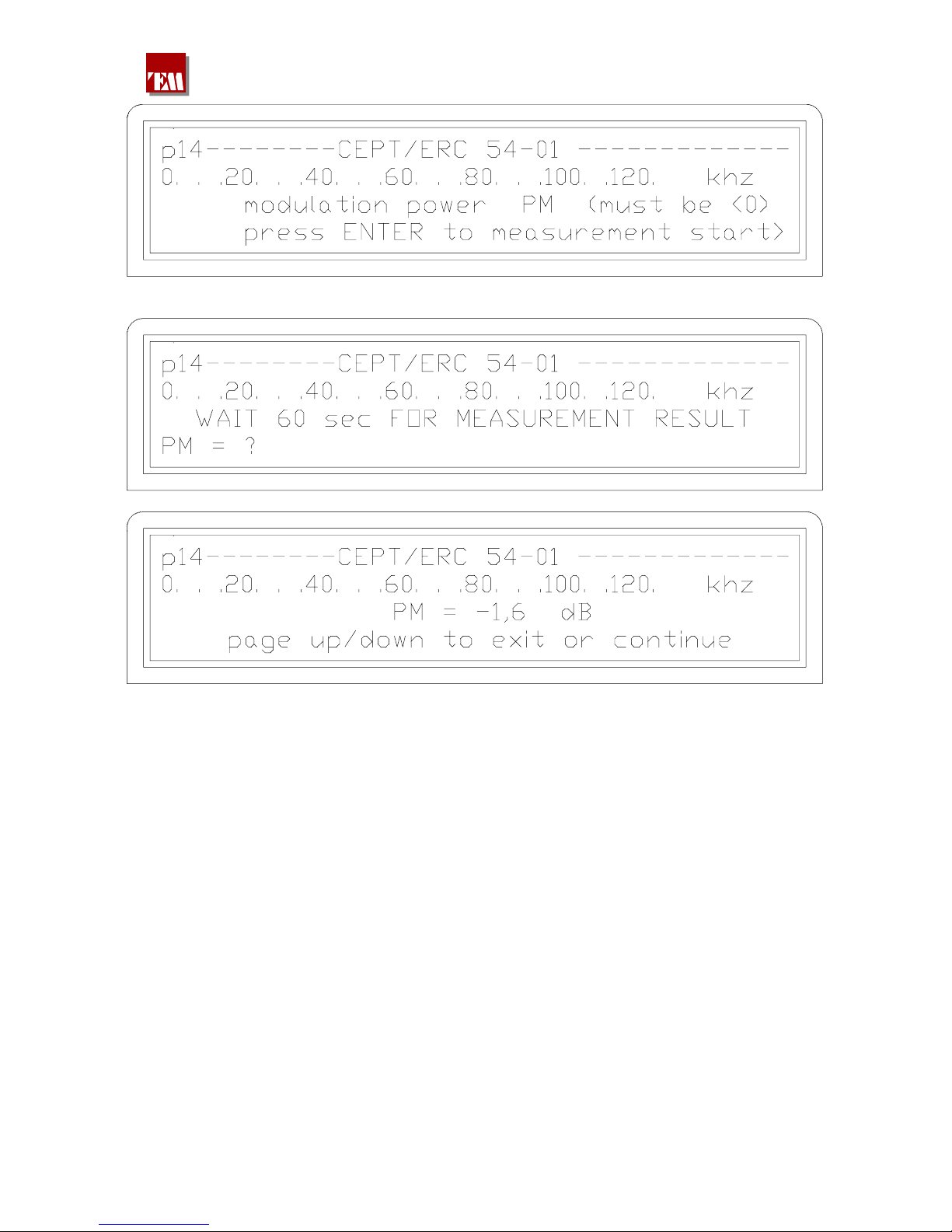
The previous eight screen shots, if selected, allow to perform the measurement of the modulation
analysis according to the CEPT 54-01rule. For an exhaustive explanation of this new measurement
method see chapter 7.
Briefly, it can be said that a music signal can exceed the limit threshold of 75kHhz, provided that
this exceeding is contained in a certain percentage. The rules concerning this topic are contained in
the above mentioned regulation and in the IEC-244. Thus it’s possible to quantify the excess of over
modulation peak and it’s possible to show, as in the appendix, that the numerical factor K fixing
this limit can not be greater than 0.2. Modulation power on the opposite can not be higher than the
one relating to a sine signal deviating 19KHz (reference =0dB)
The observation period, for the measurement and the calculation of these factors, is 1 minute, after
that the result will be displayed.
For the calculation of the K over modulation peak factor, 1200 samplings are performed during a 60
sec measurement, and the value factor is obviously 0 if no peaks exceed 75KHz. The value 0.2 is
acceptable as a higher over modulation limit; the value 0.5 shows that the modulation must be
reduced of 1dB at least, values higher than K indicates strong over modulations.
For the modulation power, over 10 millions of samplings are performed during the minute of
examination and power integral defined in the measurement segment is calculated; the result is
380 221 R02 Pag. 25
A07A2200S
compared to the one equivalent to a sine signal which deviates 19KHz; the result of the comparison
is expressed in dB and it must not be higher than 0, in order to make the measurement complying
with the rule. This limit is debatable and, as it has been described in chapter 7, normally in on-field
measurements the values of 2,3dB are found which, after all, we estimate don’t cause over
modulations.
Since the peak modulation values are random (they depend, besides on the set levels, on the type of
musical pieces as well), K or PM values can remarkably vary during the day relating to the type of
the transmitted program; it’s useful to do many measurements at different times by trying to
measure dance-music rather than spoken. By using the Personal-Computer interfaced with COM1
placed on the front panel it’s possible to perform this measurement with many hours of observation
periods as it will further be seen.
4.6.16 By entering PAGE UP the following screen shot is accessed:
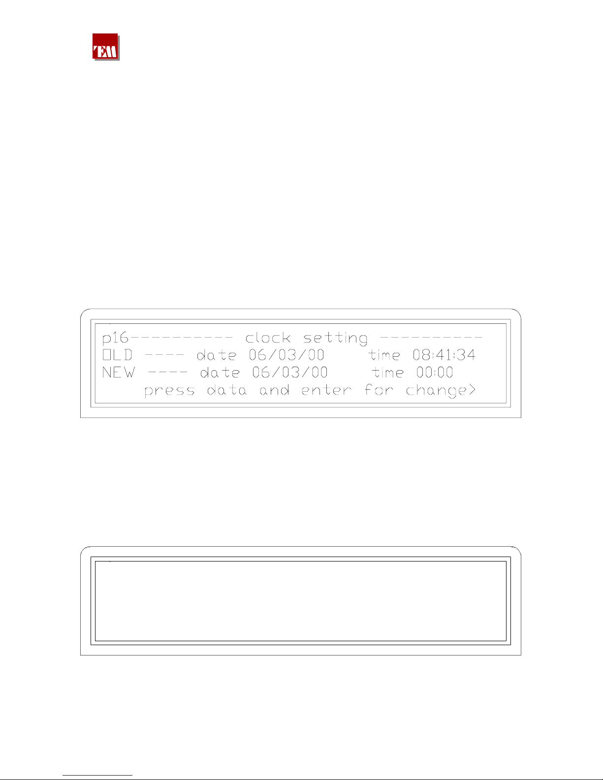
Here the transmitter internal clock which is used for the memorisation of all the events can be set.
At the top the current date appears, the new date at the bottom; in left to right order month, day,
year, hours, minutes, seconds appear.
P 17 ------------TEMPORAL POWER REDUCTION--------------------START TIME = 23:00 STOP TIME = 06:00
POWER = 1000 W POWER REDUCTION = NO
PRESS PAGE UP/DOWN TO CONTINUE >
380 221 R02 Pag. 26
A07A2200S
GSM NUMBERS SETTING FOR SMS SEND……… ..
GSM 1 = ………………………………… ... (SENT = 0)
GSM 2 = ………………………………… ... (SENT = 0)
PRESS DATA AND ENTER FOR EACH NUMBER >
TRANSMITTER SITE NAME SETTING
FOR SMS MESSAGES
SITE NAME = ………………………………… ...
PRESS DATA TO CHANGE AND ENTER >
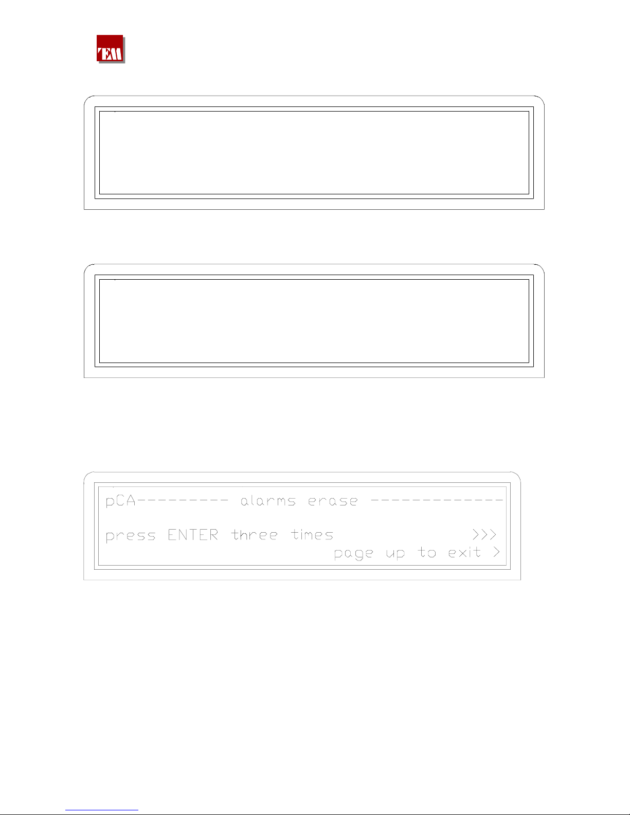
4.6.17.1 By entering PAGE UP the next page is accessed:
TO ERASE THE ALARMS AND SMS COUNTENS
By pressing three times the ENTER button, all the alarms in the memory are erased.
By entering PAGE UP, the start position is restored.
380 221 R02 Pag. 27

A07A2200S
CIRCUITS DESCRIPTION
5.1 AUDIO-IN board
The AUDIO-IN board has the task to interface the input audio signals with the modulator.
Level adjustments are performed on them, as well as pre-emphasis insertion and input
impedance selection. The outputs, going through a flat-cable to the mother board, are raised
to a high level and made balanced in order not to be interfered with the transformer flow
dispersion.
The LEFT and RIGHT signals available on the connectors placed on the rear panel enter,
after a first RF noise filter, respectively into U6 and U1. By the U11 switch and the Z1 jumper
accessible at the back, the input impedance can be selected (600? or 10k? ). A similar function is
performed by the jumpers Z3, Z4, Z5, Z6, which allow to select the input nominal value level; on
the two channels MONO examined, the switches U13 and U12 change the gain by switching three
resistances or a trimmer to put the input level to 0, 4.1, 6, 12dBm or by RT3 and RT4 to a level
between ? 2 dB respect the nominal level if the jumpers 10a ( Fig. 9d page 60 ) are in the variable
position. The signal is then the pre-emphatized; the value 50µs or 75µs is chosen by the jumper Z2,
while the possible inserting is controlled by the front keyboard. Through U3 and U4 the LEFT and
RIGHT channels output is made differential.
The MULTIPLEX external signal path is simpler. On it, it’s only adjusted the level at the
nominal value by U16, still controlled by Z3, Z4, Z5, Z6. U9 adds up the MPX signal with the two
SCA signals and generates the balanced output signal.
Normally, on the SCA signals it’s difficult to establish an input nominal level since their
contribution to the frequency deviation is variable and depends both on the number of subcarriers
between 53 and 100KHz and on the difference about MONO or STEREO transmission. In any case,
the total deviation of all the subcarriers (19KHz, SCA1, SCA2) must not exceed 10% of the
maximum nominal deviation, which in most cases is ±75KHz. If the transmitter is monophonic and
only the RDS signal placed in one of the two SCA inputs is present, the deviation level of the
transmitted data can reach ±7,5KHz; whereas if the transmitter is stereophonic and besides the RDS
signal also a lower quality audio channel on a subcarrier is present, for example at 76KHz, the total
of each subcarrier deviations can’t exceed ±7,5KHz. The stereo driving carrier will deviate ±4KHz,
the RDS signal and the other audio channel will have to deviate, for example, ±1,75KHz.
For this reason, it has been preferred to make the SCA channel levels independent between the
nominal input one of the audio channels. The adjustment is obtained by RT1 and RT2 trimmers
always placed on the rear panel.
All the set levels are showed in the display and the choice to adopt a parameters manual setting
related to the input signals level has been preferred to an easier keyboard setting to avoid a non
standard levels setting which makes the servicing or the transmitter replacement problematical. The
audio signal level errors must not be cleared on the transmitter, but at a former stage. Normally,
every broadcasting station fixes a nominal level for all signals and all the adopted equipment must
respect this sole value. As higher is this value, as higher will be the noise immunity, and the signalnoise ratio as well.
380 221 R02 Pag. 28

A07A2200S
5.2 SINTD board
SINTD board is placed at the rack centre, directly connected to the mother board from which
it can be quickly removed. It has the function of frequency synthesized oscillator (88–
108MHz) modulated by the audio composite signal.
The FET Q1 is the core of the board and oscillates at the set and controlled frequency. All the
techniques to obtain high performances in terms of noise and modulation linearity have been
adopted. Moreover for a decade T.E.M. already have been adopting these circuits solutions
(oscillators with coaxial line) for frequencies even till 3GHz for FM transmitters and audio links.
Eight varicaps DV1-DV8 modulate the oscillator being driven by the Q2 low output impedance
which reduces Nyquist this way wide band noise produced by the variable capacity diodes; at
1MHz between the carrier, the SSB noise is already better than –145dBc, in accordance to ETSETSI-300-384. The Q3 transistor reduces the flicker-noise due to the power supply; the D3-D4
series doesn’t allow the Q1 saturation, while Q4 and Q5 uncouple the oscillator from the following
amplification stages. The U14 output has a power of 10dBm.
The Q6 transistor leads the oscillator signal into the prescaler of the PLL circuit (U4); this
integrated circuit performs all the frequency synthesis functions: it’s set by U1 ports through the
main microprocessor placed on the DLCD board. The reference frequency (10MHz) is produced by
Q7; the crystal is kept at a constant temperature by a feedback obtained through U5 and U6; the
value 55°C is 5°C higher than the maximum operating temperature, so allowing to obtain a
frequency stability lower than a part per million at the environmental working range 0-45°C.
The error amplifier of the phase comparator internal to the PLL chip is composed by U13 and U2
and it has a closed loop cut frequency lower than one Hertz, so that the lowest frequencies of the
modulating stereophonic signal can maintain a separation higher than 50dB between the two
channels. The modulation, coming from the mother board and from the AUDIO-IN board, is simply
added to the VCO error voltage, no linearization has been provided to make the deviation constant
versus the output frequency; typically the deviation error is contained within 0,1 dB all over 20
MHz band.
The oscillator has been carefully shielded to avoid that close transmitters could induce spurious
frequencies on the output.
380 221 R02 Pag. 29

A07A2200S
5.3 MBA board
The central board has the task to distribute the power supplies and the input and output
signals; moreover, the audio filters and the peak-to-peak detector for the different modulation
level measurements are implemented in it.
Both the left and the right channel signals coming from the AUDIO-IN board through the J7
connector, pass through an elliptic filter made of precision active components; the bandwidth at
0.1dB is 15KHz and the attenuation over 19KHz is higher than 40dB; no adjustment is provided,
the resistances have a precision of 0.1% and the capacitors are selected and high quality type. U3,
U4, U5 and U6 make the left channel filter, the right one is symmetrical.
Another elliptic filter of an lower order clean the MULTIPLEX signal by removing the surious
signals created by the switching over 600KHz; however this is a typical L-C placed between the
two sections of U1. The two further stages formed of U2 make a phase equalizer (RT2) and a
amplitude equalizer (RT3) to compensate the DMPX board errors and the previous filter.
The operational amplifier U12 generates the composite signal by adding all the signals; the output
of the first section can either enter in the automatic gain control optional board or, in its absence, it
enters the U12 second section which acts as a clipper using the saturation and the interdiction of the
operational amplifier output circuit. The threshold value is regulated by RT6, this output of this
stage enters directly into the frequency modulator placed on the SINTD board.
The U17 switch selects the audio signal to be measured which the level is detected by a peak-topeak detector made by U13, U14, U15. Through the U18 switch, controlled by the DLCD board,
the measurement can be of peak or envelope, in accordance to the peak measurements or
modulation power.
A circuit made of U22 and U23 disables the output power in case of external command (CE) or
synthesizer fault. This function is performed through software also and this circuit represents a
security guarantee for such an important function.
5.4 AGC board
The task of this board is to guarantee the maximum allowed modulation where is not sure that the
input audio signal has a fixed value. This option can be added to the transmitter at any time and,
when it’s present, the Z3 jumper placed on the MBA board must be set to ON. Its adjustment, when
enabled, is 6dB around the nominal value and it uses 32 gain variation steps of 0.3dB each approx.
The operation is quite simple: a wide band amplifier (U6) has the gain which depends on the R2 … - R33 resistive value; these are switched by U2, U3, U4 and U5, they are controlled at their time
by the microcontroller U1. The AGCO output audio signal is detected by U7, U8 and U9 and the
peak-to-peak value is measured by the microcontroller, which consequently decides which gain
must be given to the amplifier.
The intervention time of the gain variations is not constant, but it’s for the input signal value; the
gain variation algorithm versus the time is complex in order not to distort the signal, anyhow it’s
possible to say that, when the signal has a level equal to half of the nominal one, in a couple of
minutes approximately or little bit more it’s restored to the nominal value. On the opposite, when it
has a value which is the double of the set value, it takes just few seconds to reach the nominal value.
380 221 R02 Pag. 30
 Loading...