

Page 1

xE910 Mini PCIe H ar dwar e User Guide
1vv0301006 Rev.10 – 2015-12-06
Page 2
xE910 Mini PCIe Hardware User Guide
1vv0301006 Rev.10 – 2015-12-06
Reproduction forbidden without Telit Communications S.p.A. written authorization - Al l Rights Reserved page 2 of 56
APPLICABILITY TABLE
PRODUCT
HE910 Mini PCIe
HE910-D Mini PCIe
DE910 Mini PCIe
LE910-SVG Mini PCIe
LE910-NVG Mini PCIe
LE910-NAG Mini PCIe
LE910-EUG Mini PCIe
LE910-NA V2 Mini PCIe
LE910-SV V2 Mini PCIe
LE910-EU V2 Mini PCIe
LE910-AU V2 Mini PCIe
Page 3

xE910 Mini PCIe Hardware User Guide
1vv0301006 Rev.10 – 2015-12-06
Reproduction forbidden without Telit Communications S.p.A. written authorization - Al l Rights Reserved page 3 of 56
SPECIFICATIONS SUBJECT TO CHANGE WITHOUT NOTICE
Notice
While reasonable efforts have been made to assure the accuracy of this document,
Telit assumes no liability resulting from any inaccuracies or omissions in this document,
or from use of the information obtained herein. The information in this document has
been carefully checked and is believed to be entirely reliable. However, no
responsibility is assumed for inaccuracies or omissions. Telit reser ves the right to make
changes to any products described herein and reserves the right to revise this
document and to make changes from time to time in content hereof with no obligation
to notify any person of revisions or changes. Telit does not assume any liability arising
out of the application or use of any product, software, or circuit described herein;
neither does it convey license under its patent rights or the rights of others.
It is possible that this publication may contain references to, or information about Telit
products (machines and programs), programming, or services that are not announced
in your country. Such references or information must not be construed to mean that
Telit intends to announce such Telit products, programming, or services in your
country.
Copyrights
This instruction manual and the Telit products described in this instruction manual may
be, include or describe copyrighted Telit material, such as computer programs stored in
semiconductor memories or other media. Laws in the Italy and other countries preserve
for Telit and its licensors certain exclusive rights for copyrighted material, including the
exclusive right to copy, reproduce in any form, distribute and make derivative wo rks of
the copyrighted material. Accordingly, any copyrighted material of Telit and its licensors
contained herein or in the Telit products described in this instruction manual may not be
copied, reproduced, distributed, merged or modified in any manner without the express
written permission of Telit. Furthermore, the purchase of Telit products shall not be
deemed to grant either directly or by implication, estoppel, or otherwise, any license
under the copyrights, patents or patent applications of Telit, as arises by operation of
law in the sale of a product.
Computer Software Copyrights
The Telit and 3rd Party supplied Software (SW) products described in this instruction
manual may include copyrighted Telit and other 3rd Party supplied computer programs
stored in semiconductor memories or other media. Laws in the Italy and other countries
preserve for Telit and other 3rd Party supplied SW certain exclusive rights for
copyrighted computer programs, including the exclusive right to copy or reproduce in
any form the copyrighted computer program. Accordingly, any copyrighted Telit or other
3rd Party supplied SW computer programs contained in the Telit products described in
this instruction manual may not be copied (reverse engineered) or reproduced in any
manner without the express written permission of Telit or the 3rd Party SW supplier.
Furthermore, the purchase of Telit products shall not be deemed to grant either directly
or by implication, estoppel, or otherwise, any license under the copyrights, patents or
patent applications of Telit or other 3rd Party supplied SW, except for the normal nonexclusive, royalty free license to use that arises by operation of law in the sale of a
product.
Page 4

xE910 Mini PCIe Hardware User Guide
1vv0301006 Rev.10 – 2015-12-06
Reproduction forbidden without Telit Communications S.p.A. written authorization - Al l Rights Reserved page 4 of 56
Usage and Disclosure Restrictions
License Agreements
The software described in this document is the property of Telit and its licensors. It is
furnished by express license agreement only and may be used only in accordance with
the terms of such an agreement.
Copyrighted Materials
Software and documentation are copyrighted materials. Making unauthorized copies is
prohibited by law. No part of the software or documentation may be reproduced,
transmitted, transcribed, stored in a retrieval system, or translated into any language or
computer language, in any form or by any means, without prior written permission of
Telit
High Risk Materials
Components, units, or third-party products used in the product described herein are
NOT fault-tolerant and are NOT designed, manufactured, or intended for use as on-line
control equipment in the following hazardous environments requiring fail-safe controls:
the operation of Nuclear Facilities, Aircraft Navigation or Aircraft Communication
Systems, Air Traffic Control, Life Support, or Weapons Systems (High Risk Activities").
Telit and its supplier(s) specifically disclaim any expressed or implied warranty of
fitness for such High Risk Activit ie s .
Trademarks
TELIT and the Stylized T Logo are registered in Trademark Office. All other product or
service names are the property of their respective owners.
Copyright © Telit Communications S.p.A.
Page 5

xE910 Mini PCIe Hardware User Guide
1vv0301006 Rev.10 – 2015-12-06
Reproduction forbidden without Telit Communications S.p.A. written authorization - Al l Rights Reserved page 5 of 56
Contents
1. INTRODUCTION ........................................................................................................................................................... 7
1.1. SCOPE ....................................................................................................................................................................... 7
1.2. AUDIENCE ................................................................................................................................................................. 7
1.3. CONTACT INFORMATION, SUPPORT ........................................................................................................................... 7
1.4. TEXT CONVENTIONS ................................................................................................................................................. 8
1.5. RELATED DOCUMENTS ............................................................................................................................................. 8
2. OVERVIEW .................................................................................................................................................................... 9
3. XE910 MINI PCI EXPRESS CARD CONNECTIONS............................................................................................. 10
3.1. PIN-OUT ................................................................................................................................................................ 10
3.2. ANTENNA CONNECTORS ......................................................................................................................................... 12
4. POWER SUPPLY ......................................................................................................................................................... 13
4.1. POWER SUPPLY REQUIREMENTS ............................................................................................................................. 13
4.2. POWER CONSUMPTION ............................................................................................................................................ 14
5. GSM/WCDMA/ LTE /CDMA RADIO SECTION ..................................................................................................... 15
5.1. XE910 MINI PCI PRODUCT VARIANTS .................................................................................................................... 15
5.2. TX AND RX CHARACTERISTICS ............................................................................................................................... 15
5.3. GSM/WCDMA/LTE/CDMA ANTENNA REQUIREMENTS ...................................................................................... 16
5.3.1. GSM/WCDMA/LTE/CDMA Antenna - Installation Guidelines ..................................................................... 19
5.4. ANTENNA DIVERSITY REQUIREMENTS .................................................................................................................... 21
5.5. GNSS RECEIVER ..................................................................................................................................................... 24
5.5.1. GNSS Performances ...................................................................................................................................... 24
5.5.2. GNSS RF Front End Design .......................................................................................................................... 25
6. LOGIC LEVEL SP ECIFICATIONS .......................................................................................................................... 26
7. USB PORT ..................................................................................................................................................................... 26
7.1. USB 2.0 HS ............................................................................................................................................................ 26
8. SIM INTERFACE ........................................................................................................................................................ 27
9. CONTROL SIGNALS .................................................................................................................................................. 28
9.1. WAKE# .................................................................................................................................................................. 28
9.2. W_DISABLE# ....................................................................................................................................................... 30
9.3. LED_WWAN# ....................................................................................................................................................... 30
9.4. PERST# .................................................................................................................................................................. 31
10. AUDIO SECTION OVERVIEW ............................................................................................................................ 31
10.1. ELECTRICAL CHARACTERISTICS ............................................................................................................................. 32
10.2. CODEC EXAMPLE .................................................................................................................................................. 32
11. MECHANICAL SPECIFICATIONS ..................................................................................................................... 33
11.1. WEIGHT ................................................................................................................................................................ 34
11.2. ENVIRONMENTAL REQUIREMENTS .............................................................................................................. 34
12. PACKING SYSTEM ................................................................................................................................................ 35
13. SAFETY RECOMMANDATIONS ......................................................................................................................... 36
Page 6

xE910 Mini PCIe Hardware User Guide
1vv0301006 Rev.10 – 2015-12-06
Reproduction forbidden without Telit Communications S.p.A. written authorization - Al l Rights Reserved page 6 of 56
14. CONFORMITY ASSESSMENT ISSUES .............................................................................................................. 37
14.1. 1999/5/EC DIRECTIVE (HE910) .............................................................................................................................. 37
14.2. FCC/IC REGULATORY NOTICES (HE910) ............................................................................................................... 40
14.3. 1999/5/EC DIRECTIVE (LE910) .............................................................................................................................. 42
14.4. FCC/IC REGULATORY NOTICES (LE910) ................................................................................................................ 45
14.5. CONFORMITY ASSESSMENT ISSUES / PROBLÈMES D'ÉVALUATION DE CONFORMITÉ (DE910) ................................. 48
14.6. CONFORMITY ASSESSMENT ISSUES (LE910 V2) ......................................................................................... 50
14.6.1. FCC/IC Regulatory notices ........................................................................................................................... 50
14.7. SAFETY RECOMMENDATIONS (LE910 V2) .............................................................................................................. 54
14.8. SAFETY RECOMMENDATIONS (HE910) ................................................................................................................... 55
14.9. SAFETY RECOMMENDATIONS (DE910) ................................................................................................................... 55
15. DOCUMENT HISTO RY ......................................................................................................................................... 56
Page 7
xE910 Mini PCIe Hardware User Guide
1vv0301006 Rev.10 – 2015-12-06
Reproduction forbidden without Telit Communications S.p.A. written authorization - Al l Rights Reserved page 7 of 56
1. Introduction
1.1. Scope
The aim of this document is the description of some hardware solutions useful for
developing a product with the Telit xE910 Mini PCIe Adapter.
1.2. Audience
This document is intended for Telit customers, who are integrators, about to implement
their applications using our xE910 Mini PCIe Adapter.
1.3. Contact Information, Support
For general contact, technical support, to report documentation errors and to order
manuals, contact Telit’s Technical Support Center (TTSC) at:
TS-EMEA@telit.com
TS-NORTHAMERICA@telit.com
TS-LATINAMERICA@telit.com
TS-APAC@telit.com
Alternatively, use:
http://www.telit.com/en/products/technical-support-center/contact.php
For detailed information about where you can buy the Telit modules or for
recommendations on accessories and components visit:
http://www.telit.com
To register for product news and announcements or for product questions contact
Telit’s Technical Support Center (TTSC).
Our aim is to make this guide as helpful as possible. Keep us informed of your
comments and suggestions for improvements.
Telit appreciates feedback from the users of our information.
Page 8
xE910 Mini PCIe Hardware User Guide
1vv0301006 Rev.10 – 2015-12-06
Reproduction forbidden without Telit Communications S.p.A. written authorization - Al l Rights Reserved page 8 of 56
1.4. Text Conventions
Danger – This information MUST be followed or catastrophic equipment failure or
bodily injury may occur.
Caution or Warning – Alerts the user to important points about integrating the
module, if these points are not followed, the module and end user equipment
may fail or malfunction.
Tip or Information – Provides advice and suggestions that may be useful when
integrating the module.
All dates are in ISO 8601 format, i.e. YYYY-MM-DD.
1.5. Related Documents
• HE910/UE910 AT Commands Reference Guide 80378ST10091a
• HE910 Hardware User Guide 1vv03700925
• Event Monitor Application Note 80000nt10043a
• Digital Voice Interface Application Note 80000NT10004a
• LE910 AT Commands Reference Guide 80378ST10585a
• LE910 Hardware User Guide 1vv03701089
• LE910 Digital Voice Interface Application Note 80000NT11246a
• DE910 Hardware User Guide 1vv03700951
• LE910-V2 Modules AT Commands Reference Guide 80446ST10707A
• LE910-V2 Hardware User Guide 1VV0301200
Page 9

xE910 Mini PCIe Hardware User Guide
1vv0301006 Rev.10 – 2015-12-06
Reproduction forbidden without Telit Communications S.p.A. written authorization - Al l Rights Reserved page 9 of 56
2. Overview
The aim of this document is the description of some hardware solutions useful for
developing a product that will host the Telit XE910 Mini PCIe Adapter.
In this document all the basic functions of a mobile phone will be taken into account; for
each one of them a proper hardware solution will be suggested and eventually the
wrong solutions and common errors to be avoided will be evidenced. Obviously this
document cannot embrace the whole hardware solutions and products that may be
designed. The wrong solutions to be avoided shall be considered as mandatory, while
the suggested hardware configurations shall not be considered mandatory, instead the
information given shall be used as a guide and a starting point for properly developing
your product with the Telit Mini PCIe module.
NOTICE:
(EN) The integration of the GSM/GPRS/WCDMA XE910 Mini PCIe cellular module within user
application shall be done according to the design rules described in this manual.
(IT) L’integrazione del modulo cellulare GSM/GPRS/WCDMA XE910 Mini PCIe all’interno
dell’applicazione dell’utente dovrà rispettare le indicazioni progettuali descritte in questo
manuale.
(DE) Die Integration des XE910 Mini PCIe GSM/GPRS/WCDMA Mobilfunk-Moduls in ein Gerät
muß gemäß der in diesem Dokument beschriebenen Kunstruktionsregeln erfolgen.
(SL) Integracija GSM/GPRS/WCDMA XE910 Mini PCIe modula v uporabniški aplikaciji bo
morala upoštevati projektna navodila, opisana v tem priročniku.
(SP) La utilización del modulo GSM/GPRS/WCDMA XE910 Mini PCIe debe ser conforme a los
usos para los cuales ha sido deseñado descritos en este manual del usuario.
(FR) L’intégration du module cellulaire GSM/GPRS/WCDMA XE910 Mini PCIe dans
l’application de l’utilisateur sera faite selon les règles de conception décrites dans ce manuel.
(HE)
The information presented in this document is believed to b e ac cur at e a nd r e l iable . H o wev er, no
responsibility is ass umed by Telit Communications S.p. A. for its use , nor any infringement of
patents or other ri ghts of third parties whic h may result from its use. No license is granted by
implication or other wise under any patent r ights of Telit Communicatio ns S.p.A. other than for
circuitry embodied in Telit products. This document is subject to change without notice.
Page 10
xE910 Mini PCIe Hardware User Guide
1vv0301006 Rev.10 – 2015-12-06
Reproduction forbidden without Telit Communications S.p.A. written authorization - Al l Rights Reserved page 10 of 56
3. xE910 M ini PCI express card connections
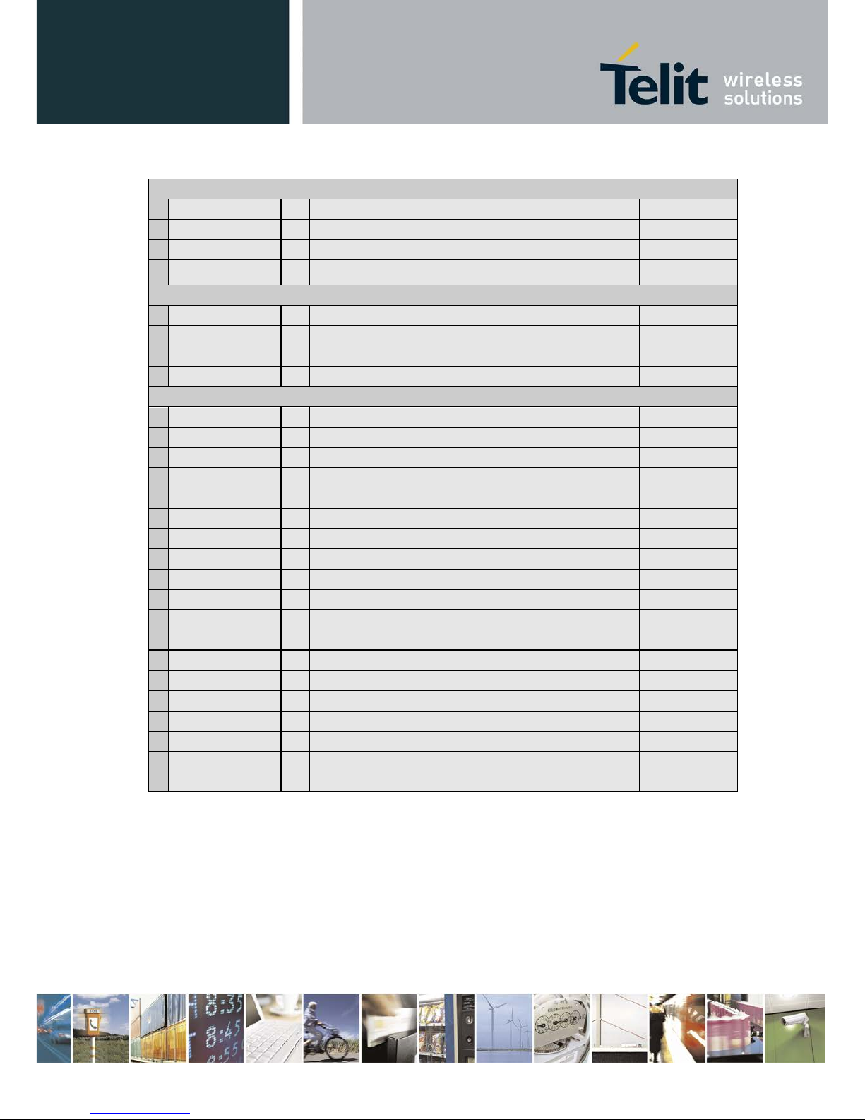
3.1. PIN-OUT
This product has a standard Mini PCI express connector, excepting the (4) audio
signals which use normally reserved connectors.
Pin Signal I/O Function Type
Power Supply
2
3V3_AUX O 3.3V supply Power
24
3V3 O 3.3V supply Power
39
3V3_AUX O 3.3V supply Power
41
3V3_AUX O 3.3V supply Power
52
3V3_AUX O 3.3V supply Power
4
GND - Ground Power
9
GND - Ground Power
15
GND - Ground Power
18
GND - Ground Power
21
GND - Ground Power
26
GND - Ground Power
27
GND - Ground Power
29
GND - Ground Power
34
GND - Ground Power
35
GND - Ground Power
37
GND - Ground Power
40
GND - Ground Power
43
GND - Ground Power
50
GND - Ground Power
SIM Card Interface
8
SIMVCC O External SIM signal – Power supply for the SIM 1.8 / 3V
10
SIMIO I/O External SIM signal - Data I/O 1.8 / 3V
12
SIMCLK O External SIM signal – Clock 1.8 / 3V
14
SIMRST O External SIM signal – Reset 1.8 / 3V
USB
36
USB D- I/O USB differential Data (-) 0.3…2.8V
38
USB D+ I/O USB differential Data (+) 0.3…2.8V
Pi
n
Signal I/O Function Type
Page 11
xE910 Mini PCIe Hardware User Guide
1vv0301006 Rev.10 – 2015-12-06
Reproduction forbidden without Telit Communications S.p.A. written authorization - Al l Rights Reserved page 11 of 56
Miscellaneous Functions
1
WAKE# O Active low signal used to wake up the system from stand-by 3.3V
20
WDISABLE# I Active low signal for wireless disabling (Flight mode) 3.3V
22
PERST# I Active low functional reset to the card 3.3V
42
LED_WWAN# O
Active low, open drain signal for WWAN LED driving, used to provide
module’s status indication
3.3V…5V
Digital Voice Interface (DVI)
45
PCM_CLK I/O Digital Audio Interface (CLK) CMOS 1.8V
47
PCM_RX I Digital Audio Interface (RX) CMOS 1.8V
49
PCM_TX O Digital Audio Interface (TX) CMOS 1.8V
51
PCM_SYNC I/O Digital Audio Interface (SYNC) CMOS 1.8V
N.C.
3
-
5
-
6
-
7
-
11
-
13
-
16
-
17
-
19
-
23
-
25
-
28
-
30
-
31
-
32
-
33
-
44
-
46
-
48
-
Page 12

xE910 Mini PCIe Hardware User Guide
1vv0301006 Rev.10 – 2015-12-06
Reproduction forbidden without Telit Communications S.p.A. written authorization - Al l Rights Reserved page 12 of 56
3.2. Antenna Connectors
The xE910 Mini PCIe adapter is equipped with a set of 50 Ω RF U.FL. connectors from
Hirose U.FL-R-SMT-1(10).
The available connectors are:
• Main RF antenna (ANT)
• RX Diversity Antenna (DIV)
• GNSS Antenna (GPS)
See the picture on the right for their position on
the interface.
The presence of all the connectors is depending
on the product characteristics and supported
functionalities.
For more information about mating connectors, visit the website
http://www.hirose-connectors.com/
Page 13
xE910 Mini PCIe Hardware User Guide
1vv0301006 Rev.10 – 2015-12-06
Reproduction forbidden without Telit Communications S.p.A. written authorization - Al l Rights Reserved page 13 of 56
4. Power Supply
The power supply circuitry and board layout are a very important part in the full product
design and they strongly reflect on the product overall performances, hence read the
requirements carefully and the guidelines that will follow for a proper design.
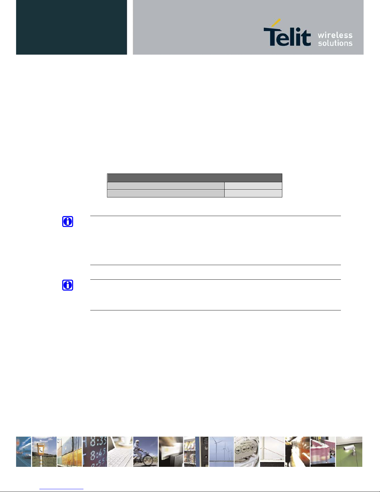
4.1. Power Supply Requirements
The external power supply must be connected to the pins 2, 39, 41, 52 and must fulfill
the following requirements:
POWER SUPPLY
Nominal Supply Voltage
3.3 V
Normal Operating Voltage Range
3.00 V÷ 3.60 V
NOTE:
The Operating Voltage Range MUST never be exceeded; care must be taken when
designing the application’s power supply section to avoid having an excessive voltage
drop.
If the voltage drop is exceeding the limits it could cause a Power Off of the module.
NOTE:
Overshoot voltage (regarding MAX Operating Voltage) and drop in voltage (regarding
MIN Operating Voltage) MUST never be exceeded;
Page 14
xE910 Mini PCIe Hardware User Guide
1vv0301006 Rev.10 – 2015-12-06
Reproduction forbidden without Telit Communications S.p.A. written authorization - Al l Rights Reserved page 14 of 56
4.2. Power Consumption
Please refer to the Module’s Hardware User guide for the details
The GSM system is made in a way that the RF transmission is not continuous, else it is
packed into bursts at a base frequency of about 216 Hz, and the relative current peaks
can be as high as about 2.4A. Therefore the power supply has to be designed in order
to withstand with these current peaks without big voltage drops; this means that both
the electrical design and the board layout must be designed for this current flow. If the
voltage drop during the peak current absorption is too much, then the device may even
shutdown as a consequence of the supply voltage drop.
NOTE:
The electrical design for the Power supply should be made ensuring it will be capable
of a peak current output of at least 2.4 A.
Page 15
xE910 Mini PCIe Hardware User Guide
1vv0301006 Rev.10 – 2015-12-06
Reproduction forbidden without Telit Communications S.p.A. written authorization - Al l Rights Reserved page 15 of 56
5. GSM/WCDMA/LTE /CDMA Radio Secti on
5.1. xE910 Mini PCI Product Variants
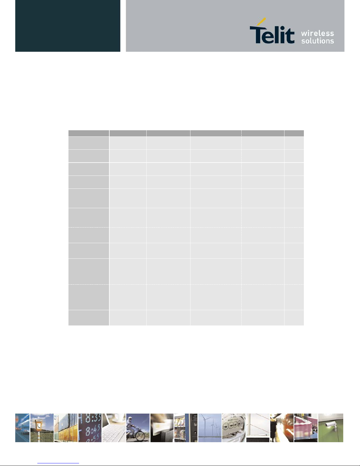
The following table is listing the main differences between the xE910 variants:
Product
2G Bands
3G Bands
LTE Bands
CDMA Bands
GNSS
LE910-NA V2
Not
supported
B5, B2
B2, B4, B5,
B12/B17 (B13)
NO
NO
LE910-SV V2
Not
supported
Not supported B2, B4, B13 NO
NO
LE910-EU V2
GSM 900,
DCS1800
B1, B8
B3, B7, B20, B1,
B8
NO
NO
LE910-AU V2
Not
supported
Not supported B3, B7, B28 NO
NO
LE910-EUG
GSM 900,
DCS1800
B5(850), B8
(900), B1
(2100)
B20 (800), B3
(1800), B7 (2600)
NO YES
LE910-NAG
GSM 850,
PCS 1900
B5(850),
B2(1900)
B17(700), B5(850),
B4(1700),
B2(1900)
NO YES
LE910-NVG
Not
supported
B5(850),
B2(1900)
B13(700),
B4(1700)
NO YES
LE910-SVG
Not
supported
Not supported
B13(700),
B4(1700)
NO YES
HE910
GSM 850,
GSM 900,
DCS1800,
PCS 1900
FDD B1, B2,
B4, B5, B8
Not supported NO YES
HE910-D
GSM 850,
GSM 900,
DCS1800,
PCS 1900
FDD B1, B2,
B4, B5, B8
Not supported NO NO
DE910-DUAL
Not
supported
Not supported Not supported BC0, BC1 YES
5.2. TX and RX characteristics
Please refer to the Module’s Hardware User guide for the details
Page 16
xE910 Mini PCIe Hardware User Guide
1vv0301006 Rev.10 – 2015-12-06
Reproduction forbidden without Telit Communications S.p.A. written authorization - Al l Rights Reserved page 16 of 56
5.3. GSM/WCDMA/LTE/CDMA Antenna Requirements
The antenna connection is one of the most important aspect in the full product design
as it strongly affects the product overall performances, hence read carefully and follow
the requirements and the guidelines for a proper design.
The xE910 Mini PCIe adapter is provided with three RF connectors.
The available connectors are:
• Main RF antenna (ANT)
• RX Diversity Antenna (DIV)
• GNSS Antenna (GPS)
Connecting cables between the module and the antenna must have 50 Ω impedance.
If the impedance of the module is mismatched, RF performance is reduced
significantly.
If the host device is not designed to use the module’s diversity or GPS antenna,
terminate the interface with a 50Ω load.
MAIN ANTENNA REQUIREMENTS for LE910-N A V 2
Frequency range
Depending by frequency band(s) provided by the network
operator, the customer shall use the most suitable antenna for
that/those band(s)
Bandwidth
140 MHz in LTE/WCDMA Band 2
445 MHz in LTE Band 4
70 MHz in LTE/WCDMA Band 5
80 MHz in LTE Band 8 / GSM900
47 MHz in LTE Band 12
41 MHz in LTE Band 13
42 MHz in LTE band 17
Impedance
50 ohm
Input power
> 24dBm Average power in WCDMA & LTE
VSWR absolute max
≤ 10:1 (limit to avoid permanent damage)
VSWR recommended
≤ 2:1 (limit to fulfil all regulatory requirements)
MAIN ANTENNA REQUIREMENTS for LE910-AU V2
Frequency range
Depending by frequency band(s) provided by the network
operator, the customer shall use the most suitable antenna for
that/those band(s)
Bandwidth
170 MHz in LTE Band 3
190 MHz in LTE Band 7
100 MHz in LTE Band 28
Impedance
50 ohm
Input power
> 24dBm Average power in WCDMA & LTE
VSWR absolute max
≤ 10:1 (limit to avoid permanent damage)
VSWR recommended
≤ 2:1 (limit to fulfil all regulatory requirements)
Page 17
xE910 Mini PCIe Hardware User Guide
1vv0301006 Rev.10 – 2015-12-06
Reproduction forbidden without Telit Communications S.p.A. written authorization - Al l Rights Reserved page 17 of 56
MAIN ANTENNA REQUIREMENTS for LE910-EU V2
Frequency range
Depending by frequency band(s) provided by the network
operator, the customer shall use the most suitable antenna for
that/those band(s)
Bandwidth
250 MHz in LTE/WCDMA Band 1
170 MHz in LTE/WCDMA Band 3 / DCS1800
190 MHz in LTE Band 7
80 MHz in LTE/WCDMA Band 8 / GSM900
71 MHz in LTE Band 20
Impedance
50 ohm
Input power
> 24dBm Average power in WCDMA & LTE
VSWR absolute max
≤ 10:1 (limit to avoid permanent damage)
VSWR recommended
≤ 2:1 (limit to fulfil all regulatory requirements)
MAIN ANTENNA REQUIREMENTS for LE910-EUG
Frequency range
Depending by frequency band(s) provided by the network
operator, the customer shall use the most suitable antenna for
that/those band(s)
Bandwidth (GSM/EDGE)
GSM900 : 80 MHz
GSM1800(DCS) : 170 MHz
Bandwidth
(WCDMA)
WCDMA band I(2100) : 250 MHz
WCDMA band V(850) : 70 MHz
WCDMA band VIII(900) : 80 MHz
Bandwidth
(LTE)
LTE band III(1800) : 170 MHz
LTE Band VII(2600) : 190 MHz
LTE Band XX(800) : 71 MHz
Impedance
50 ohm
Input power
> 33dBm(2 W) peak power in GSM
> 24dBm Average power in WCDMA & LTE
VSWR absolute max
≤ 10:1 (limit to avoid permanent damage)
VSWR recommended
≤ 2:1 (limit to fulfil all regulatory requirements)
Page 18

xE910 Mini PCIe Hardware User Guide
1vv0301006 Rev.10 – 2015-12-06
Reproduction forbidden without Telit Communications S.p.A. written authorization - Al l Rights Reserved page 18 of 56
MAIN ANTENNA REQUIREMENTS for LE910-NAG
Frequency range
Depending by frequency band(s) provided by the network
operator, the customer shall use the most suitable antenna for
that/those band(s)
Bandwidth (GSM/EDGE)
GSM850 : 70 MHz
GSM1900(PCS) : 140 MHz
Bandwidth
(WCDMA)
WCDMA band II(1900) : 140 MHz
WCDMA band V(850) : 70 MHz
Bandwidth
(LTE)
LTE Band II(1900) : 140 MHz
LTE Band IV(1700) : 445 MHz
LTE Band V (850) : 70 MHz
LTE Band XVII(700) : 42 MHz
Impedance
50 ohm
Input power
> 33dBm(2 W) peak power in GSM
> 24dBm Average power in WCDMA & LTE
VSWR absolute max
≤ 10:1 (limit to avoid permanent damage)
VSWR recommended
≤ 2:1 (limit to fulfil all regulatory requirements)
MAIN ANTENNA REQUIREMENTS for LE910-NVG
Frequency range
Depending by frequency band(s) provided by the network
operator, the customer shall use the most suitable antenna for
that/those band(s)
Bandwidth
(WCDMA)
WCDMA band II(1900) : 140 MHz
WCDMA band V(850) : 70 MHz
Bandwidth
(LTE)
LTE Band IV(1700) : 445 MHz
LTE Band XIII(700) : 41 MHz
Impedance
50 ohm
Input power
> 24dBm Average power in WCDMA & LTE
VSWR absolute max
≤ 10:1 (limit to avoid permanent damage)
VSWR recommended
≤ 2:1 (limit to fulfil all regulatory requirements)
MAIN ANTENNA REQUIREMENTS for LE910-SVG
Frequency range
Depending by frequency band(s) provided by the network
operator, the customer shall use the most suitable antenna for
that/those band(s)
Bandwidth
(LTE)
LTE Band IV(1700) : 445 MHz
LTE Band XIII(700) : 41 MHz
Impedance
50 ohm
Input power
> 24dBm Average power
VSWR absolute max
≤ 10:1 (limit to avoid permanent damage)
VSWR recommended
≤ 2:1 (limit to fulfil all regulatory requirements)
Page 19

xE910 Mini PCIe Hardware User Guide
1vv0301006 Rev.10 – 2015-12-06
Reproduction forbidden without Telit Communications S.p.A. written authorization - Al l Rights Reserved page 19 of 56
MAIN ANTENNA REQUIREMENTS for HE910
Frequency range
Depending by frequency band(s) provided by the network
operator, the customer shall use the most suitable antenna for
that/those band(s)
Bandwidth (GSM/EDGE)
70 MHz in GSM850, 80 MHz in GSM900, 170 MHz in DCS & 140
MHz PCS band
Bandwidth
(WCDMA)
70 MHz in WCDMA Band V
80 MHz in WCDMA Band VIII
460 MHz in WCDMA Band IV
140 MHz in WCDMA Band II
250 MHz in WCDMA Band I
Impedance
50 ohm
Input power
> 33dBm(2 W) peak power in GSM
> 24dBm Average power in WCDMA
VSWR absolute max
≤ 10:1 (limit to avoid permanent damage)
VSWR recommended
≤ 2:1 (limit to fulfil all regulatory requirements)
MAIN ANTENNA REQUIREMENTS for DE910 -DUAL
Frequency range
Depending by frequency band(s) provided by the network
operator, the customer shall use the most suitable antenna for
that/those band(s)
Bandwidth
70 MHz in CDMA BC0
140 MHz in CDMA BC1
Gain
Gain < 5.12dBi in CDMA BC0
Gain < 6.12dBi in CDMA BC1
Impedance
50 ohm
Input power
> 24.4dBm Average Power in CDMA
VSWR absolute max
≤ 5:1 (Limit to avoid permanent damage)
VSWR recommended
≤ 2:1 (limit to fulfil all regulatory requirements)
Please refer to the Module’s Hardware User guide for the details
5.3.1. GSM/WCDMA/LTE/CDMA Antenna - Installation Guidelines
• Install the antenna in a place covered by the GSM/WCDMA/LTE/CDMA signal.
• If the device antenna is located greater then 20cm from the human body and there
are no co-located transmitters t hen the Telit FCC/IC approvals can be re-used by
the end product
• If the device antenna is located less than 20cm from the human body or there are no
co-located transmitters then the additional FCC/IC testing may be required for the
end product (Telit FCC/IC approvals cannot be reused)
• Antenna shall not be installed inside metal cases
• Antenna shall be installed also according antenna manufacturer instructions.
Page 20

xE910 Mini PCIe Hardware User Guide
1vv0301006 Rev.10 – 2015-12-06
Reproduction forbidden without Telit Communications S.p.A. written authorization - Al l Rights Reserved page 20 of 56
Page 21

xE910 Mini PCIe Hardware User Guide
1vv0301006 Rev.10 – 2015-12-06
Reproduction forbidden without Telit Communications S.p.A. written authorization - Al l Rights Reserved page 21 of 56
5.4. Antenna Diversity Requirements
This product includes an input for a second RX antenna to improve the radio sensitivity.
The function is called Antenna Diversity.
DIVERSITY ANTENNA REQUIREMENTS for LE910-NA V2
Frequency range
Depending by frequency band(s) provided by the network
operator, the customer shall use the most suitable antenna for
that/those band(s)
Bandwidth
60 MHz in LTE/WCDMA Band 2
45 MHz in LTE Band 4
25 MHz in LTE/WCDMA Band 5
35 MHz in LTE Band 8 / GSM900
15 MHz in LTE Band 12
10 MHz in LTE Band 13
12 MHz in LTE band 17
Impedance
50 ohm
VSWR recommended
≤ 2:1 (limit to fulfil all regulatory requirements)
DIVERSITY ANTENNA REQUIREMENTS for LE910-SV V2
Frequency range
Depending by frequency band(s) provided by the network
operator, the customer shall use the most suitable antenna for
that/those band(s)
Bandwidth
60 MHz in LTE/WCDMA Band 2
45 MHz in LTE Band 4
10 MHz in LTE Band 13
Impedance
50 ohm
VSWR recommended
≤ 2:1 (limit to fulfil all regulatory requirements)
DIVERSITY ANTENNA REQUIREMENTS for LE910-AU V2
Frequency range
Depending by frequency band(s) provided by the network
operator, the customer shall use the most suitable antenna for
that/those band(s)
Bandwidth
75 MHz in LTE Band 3
70 MHz in LTE Band 7
45 MHz in LTE Band 28
Impedance
50 ohm
VSWR recommended
≤ 2:1 (limit to fulfil all regulatory requirements)
Page 22

xE910 Mini PCIe Hardware User Guide
1vv0301006 Rev.10 – 2015-12-06
Reproduction forbidden without Telit Communications S.p.A. written authorization - Al l Rights Reserved page 22 of 56
DIVERSITY ANTENNA REQUIREMENTS for LE910-EU V2
Frequency range
Depending by frequency band(s) provided by the network
operator, the customer shall use the most suitable antenna for
that/those band(s)
Bandwidth
60 MHz in LTE/WCDMA Band 1
75 MHz in LTE/WCDMA Band 3 / DCS1800
70 MHz in LTE Band 7
35 MHz in LTE/WCDMA Band 8 / GSM900
30 MHz in LTE Band 20
Impedance
50 ohm
VSWR recommended
≤ 2:1 (limit to fulfil all regulatory requirements)
DIVERSITY ANTENNA REQUIREMENTS for LE910-EUG
Frequency range
Depending by frequency band(s) provided by the network
operator, the customer shall use the most suitable antenna for
that/those band(s)
Bandwidth
(WCDMA)
WCDMA band I(2100) : 250 MHz
WCDMA band V(850) : 70 MHz
WCDMA band VIII(900) : 80 MHz
Bandwidth
(LTE)
LTE band III(1800) : 170 MHz
LTE Band VII(2600) : 190 MHz
LTE Band XX(800) : 71 MHz
Impedance
50 ohm
VSWR recommended
≤ 2:1 (limit to fulfil all regulatory requirements)
DIVERSITY ANTENNA REQUIREMENTS for LE910-NAG
Frequency range
Depending by frequency band(s) provided by the network
operator, the customer shall use the most suitable antenna for
that/those band(s)
Bandwidth
(WCDMA)
WCDMA band II(1900) : 140 MHz
WCDMA band V(850) : 70 MHz
Bandwidth
(LTE)
LTE Band II(1900) : 140 MHz
LTE Band IV(1700) : 445 MHz
LTE Band V (850) : 70 MHz
LTE Band XVII(700) : 42 MHz
Impedance
50 ohm
VSWR recommended
≤ 2:1 (limit to fulfil all regulatory requirements)
Page 23

xE910 Mini PCIe Hardware User Guide
1vv0301006 Rev.10 – 2015-12-06
Reproduction forbidden without Telit Communications S.p.A. written authorization - Al l Rights Reserved page 23 of 56
DIVERSITY ANTENNA REQUIREMENTS for LE910-NVG
Frequency range
Depending by frequency band(s) provided by the network
operator, the customer shall use the most suitable antenna for
that/those band(s)
Bandwidth
(WCDMA)
WCDMA band II(1900) : 140 MHz
WCDMA band V(850) : 70 MHz
Bandwidth
(LTE)
LTE Band IV(1700) : 445 MHz
LTE Band XIII(700) : 41 MHz
Impedance
50 ohm
VSWR recommended
≤ 2:1 (limit to fulfil all regulatory requirements)
DIVERSITY ANTENNA REQUIREMENTS for LE910-SVG
Frequency range
Depending by frequency band(s) provided by the network
operator, the customer shall use the most suitable antenna for
that/those band(s)
Bandwidth
(LTE)
LTE Band IV(1700) : 445 MHz
LTE Band XIII(700) : 41 MHz
Impedance
50 ohm
VSWR recommended
≤ 2:1 (limit to fulfil all regulatory requirements)
DIVERSITY ANTENNA REQUIREMENTS for HE910
Frequency range
Depending by frequency band(s) provided by the network
operator, the customer shall use the most suitable antenna for
that/those band(s)
Bandwidth (GSM/EDGE)
70 MHz in GSM850, 80 MHz in GSM900 & 140 MHz PCS band
Bandwidth
(WCDMA)
70 MHz in WCDMA Band V
80 MHz in WCDMA Band VIII
140 MHz in WCDMA Band II
250 MHz in WCDMA Band I
Impedance
50 ohm
VSWR recommended
≤ 2:1 (limit to fulfil all regulatory requirements)
DIVERSITY ANTENNA REQUIREMENTS for DE910-DUAL
Frequency range
Depending by frequency band(s) provided by the network
operator, the customer shall use the most suitable antenna for
that/those band(s)
Bandwidth
70 MHz in CDMA BC0
140 MHz in CDMA BC1
Impedance
50 ohm
VSWR recommended
≤ 2:1 (limit to fulfil all regulatory requirements)
Page 24

xE910 Mini PCIe Hardware User Guide
1vv0301006 Rev.10 – 2015-12-06
Reproduction forbidden without Telit Communications S.p.A. written authorization - Al l Rights Reserved page 24 of 56
The second Rx antenna should not be located in the close vicinity of main antenna. In
order to improve Diversity Gain, Isolation and reduce mutual interaction, the two
antennas should be located at the maximum reciprocal distance possible, taking into
consideration the available space in the application.
NOTE1:
On HE910 the diversity is not supported on the FDD BAND IV and DCS band.
NOTE2:
In case of HE910, if the RX Diversity is not used/connected, disable the Diversity
functionality using the AT#RXDIV command (ref to the At User guide for the proper
syntax).
5.5. GNSS Receiver
The XE910 Mini PCIe adapter integrates a GNSS receiver that could be used in
Standalone mode and in A-GPS (assisted GPS), according to the different
configurations.
The supported technologies are described in the following table:
Product
GPS
GLONASS
LE910-EUG
YES YES
LE910-NAG
YES YES
LE910-NVG
YES YES
LE910-SVG
YES YES
HE910
YES NO
HE910-D
NO NO
DE910-DUAL
YES YES
LE910-NA V2
NO NO
LE910-SV V2
NO NO
LE910-EU V2
NO NO
LE910-AU V2
NO NO
5.5.1. GNSS Performances
Please refer to the Module’s Hardware User guide for the details
Page 25

xE910 Mini PCIe Hardware User Guide
1vv0301006 Rev.10 – 2015-12-06
Reproduction forbidden without Telit Communications S.p.A. written authorization - Al l Rights Reserved page 25 of 56
5.5.2. GNSS RF Front End Design
The xE910 Mini PCIe adapter contains an integrated LNA and pre-select SAW filter.
This allows the module to work well with a passive GPS antenna. If the antenna cannot
be located near the xE910, then an active antenna (that is, an antenna with a low noise
amplifier built in) can be used with an external dedicated power supply circuit.
NOTE:
Please refer to the Module’s Hardware User Guide for detailed information about GPS
operating modes and RF signal requirements.
Page 26

xE910 Mini PCIe Hardware User Guide
1vv0301006 Rev.10 – 2015-12-06
Reproduction forbidden without Telit Communications S.p.A. written authorization - Al l Rights Reserved page 26 of 56
6. Logic level specifications
The following table shows logic level specifications used in the xE910 interface circuits:
Absolute Maximum Ratings -Not Functional
Parameter
Min
Max
Input level on any digital pin (CMOS 1.
with respect to ground
-0.5V
3.6V
Operating Range – DC Specification for 3V3 Logic Signalling
Symbol
Parameter
Min
Max
3V3, 3V3_AUX Supply voltage
3.0V
3.6V
VIH Input high level
2.0V
3.6V
VIL Input low level
-0.5V
0.8V
VOH Output high level
2.0V
3.6V
VOL Output low level
-0.5V
0.8V
IIN
Input Leakage
Current
-10µA
10µA
IOL
Output Low Current
for open-drain
signals
4mA
7. USB Port
The xE910 Mini PCIe adapter includes one integrated universal serial bus (USB)
transceiver, compliant with the standard USB 2.0 for high speed (HS) operations.
7.1. USB 2.0 HS
This port is compliant with the USB 2.0 specifications.
The following table lists the available signals:
PAD Signal I/O Function Type
38
USB_D+ I/O USB differential Data (+) 0.3…2.8V
36
USB_D- I/O USB differential Data (-) 0.3…2.8V
The USB interface is powered directly from the 3V3 supply.
Page 27

xE910 Mini PCIe Hardware User Guide
1vv0301006 Rev.10 – 2015-12-06
Reproduction forbidden without Telit Communications S.p.A. written authorization - Al l Rights Reserved page 27 of 56
8. SIM interface
The SIM pins provide the connections necessary to interface to a SIM socket located
on the host device. Voltage levels over this interface comply with 3GPP standards.
SIM Card Interface
8
SIMVCC O External SIM signal – Power supply for the SIM 1.8 / 3V
10
SIMIO I/O External SIM signal - Data I/O 1.8 / 3V
12
SIMCLK O External SIM signal – Clock 1.8 / 3V
14
SIMRST O External SIM signal – Reset 1.8 / 3V
Following picture depicts the external SIM recommended connections:
NOTE: D O NOT TERMINAT E PI NS 8, 10, 12, 14 WHEN USING MODEL INCLUDING
SIM CARD HOLDER.
Page 28

xE910 Mini PCIe Hardware User Guide
1vv0301006 Rev.10 – 2015-12-06
Reproduction forbidden without Telit Communications S.p.A. written authorization - Al l Rights Reserved page 28 of 56
9. Control signals
The XE910 Mini PCIe provides signals for module control, as described in the following
table:
Pin Signal I/O Function Type
1
WAKE# O Active low signal used to wake up the system from stand-by 3.3V
20
W_DISABLE# I Act i ve l ow signal for wireles s disabling (Ai rpl ane mode) 3.3V
22
PERST# I Active low functional reset to the card 3.3V
42
LED_WWAN# O
Active low, open drain signal for WWAN LED driving, used
to provide module’s status indication
3.3V…5V
9.1. WAKE#
WAKE# is driven, by default, by the module according the PCI Express Mini Card
Electromechanical Specification Revision 1.2.
NOTE: WAKE# IS NOT SUPPORTED IN HOST USING PCI EXPRESS MINI CARD
ELECTROMECHANICAL SPECIFI CAT ION REVISION 1.1 AND BELOW.
NOTE: THIS SIGNAL IS NOT ACTIVE BY DEFAULT. I F DESIRED IT CAN BE
CONFIGURED REMAPPING AN EVENT UNDER MONITORING THROUGH
AT#EVMONI. FOR DETAILS REFER TO THE AT COMMAND USER GUIDE
Page 29

xE910 Mini PCIe Hardware User Guide
1vv0301006 Rev.10 – 2015-12-06
Reproduction forbidden without Telit Communications S.p.A. written authorization - Al l Rights Reserved page 29 of 56
Following picture shows the internal WAKE# driver:
WAKE# output may be connected to an edge sensitive application input (e.g. a
microcontroller input with IRQ enabled). No external pull-up is needed, since it is
internally implemented.
EXAMPLE: In the following example, a RING monitor activates the WAKEUP signal. (cf.
Event Monitor App.Note 80000n t10 043 a)
AT#ENAEVMONI=0 //disable all events
AT#GPIO=3,0,1 //Set GPIO3=>’0’, “WAKE signal reset”
AT#ENAEVMONICFG=3,1,2 //AT port setting
AT#EVMONI="RING",0,1,3 //event 0-RING, after 3 rings
AT#EVMONI="RING",0,0,"AT#GPIO=3,1,1" //GPIO3=>’1’, “WAKE signal active”
AT#EVMONI=”RING”,1 //event 0-RING enabled
AT#EVMONI="GPIO1",1,1,3 //event 1-GPIO3
AT#EVMONI="GPIO1",1,2,1 //when goes hi
AT#EVMONI="GPIO1",1,3,5 //after 5s
AT#EVMONI="GPIO1",1,0," AT#GPIO=3,0,1" //Set GPIO3=>’0’, “WAKE signal
reset”
AT#EVMONI="GPIO1",1 //event 1-GPIO3 enabled
AT#ENAEVMONI=1 //enable all events
Page 30

xE910 Mini PCIe Hardware User Guide
1vv0301006 Rev.10 – 2015-12-06
Reproduction forbidden without Telit Communications S.p.A. written authorization - Al l Rights Reserved page 30 of 56
9.2. W_DISABLE#
W_DISABLE# is used to force the module to shut down. Thanks to its internal pull-up,
leaving this pin unconnected allows the module to operate normally. This switch follows
the behavior as described in the PCI-Express Mini Card specification.
9.3. LED_WWAN#
LED_WWAN# is driven, by default, by the module according the PCI Express Mini Card
Electromechanical Specification Revision 1.1. If desired, LED behavior can be
configured by adjusting software settings. The following picture shows the internal
LED_WWAN# driver and its recommended connection to a LED:
R
x
should be dimensioned according to typical voltage drop on application LED and to
its supply voltage (3V3 to 5V).
NOTE: THIS SIGNAL IS NOT ACTIVE BY DEFAULT. REFER TO AT#SLED
DESCRIPTION IN THE AT COMMAND USER GUIDE
Page 31

xE910 Mini PCIe Hardware User Guide
1vv0301006 Rev.10 – 2015-12-06
Reproduction forbidden without Telit Communications S.p.A. written authorization - Al l Rights Reserved page 31 of 56
9.4. PERST#
Reset Signal
Signal
Function
I/O
Pin
PERST# *
Phone reset
I
22
PERST# * is used to reset the xE910. W henever this signal is pulled low, the xE910 is
reset. When the device is reset it stops any operation. After the release of the reset the
xE910 is unconditionally restarted, without doing any detach operation from the network
where it is registered. The reset signal must not be used to normally restart the device,
but only as an emergency exit in the rare case the device remains stuck waiting for
some network response.
PERST#* is internally controlled on start-up to achieve a proper power-on reset
sequence, so there's no need to control this pin on start-up. It may only be used to
reset a device already on that is not responding to any command.
NOTE:
Do not use this signal to power cycle the xE910 Mini PCIe. Use the AT#SHDN
command instead.
Reset Signal Operating levels:
Signal
Min
Max
RESET Input high
2.0V
3.6V
RESET Input low
-0.5V
0.8V
* this signal is not internally pulled up so an external pull-up is required whenever the
pin is not used.
If PERST# is used, t hen it must always be connected to a push-pull output in order
to allow the internal circuitry to correctly execute power on reset and under voltage
lockout functions.
10. Audio Section Overview
The xE910 Module does not provide an Analog Audio section.
One DIGITAL AUDIO bus is available.
In order to develop an application including an Analog Audio it is necessary to add a
Page 32

xE910 Mini PCIe Hardware User Guide
1vv0301006 Rev.10 – 2015-12-06
Reproduction forbidden without Telit Communications S.p.A. written authorization - Al l Rights Reserved page 32 of 56
dedicated CODEC on the Application design.
10.1. Electrical Characteristics
The product provides a PCM Digital Audio Interface (DVI) on the following Pins:
Digital Voice Interface (DVI)
45
PCM_CLK I/O Digital Audio Interface (CLK) CMOS 1. 8V
47
PCM_RX I Digital Audio Interface (RX) CMOS 1.8V
49
PCM_TX O Digital Audio Interface (TX) CMOS 1.8V
51
PCM_SYNC I/O Digital Audio Interface (SYNC) CMOS 1.8V
More details on the use of digital audio can be found in Module’s DVI application Note.
NOTE: T HESE SIGNALS ARE 1.8V, NOT COMPATIBLE WITH Mini PCIe BUSES.
THIS IS AN ADVANCED VOICE FUNCTIO NALITY AND THE HOST SHOULD TAKE
CARE OF CORRECT COMPATIBILITY.
10.2. CODEC Example
Please refer to the Module’s Digital Voice Application Note
Page 33

xE910 Mini PCIe Hardware User Guide
1vv0301006 Rev.10 – 2015-12-06
Reproduction forbidden without Telit Communications S.p.A. written authorization - Al l Rights Reserved page 33 of 56
11. Mechanical specifications
The xE910 Mini PCIe adapters have been designed to be compliant with a standard
lead-free SMT process.
Moreover, it is compatible with the Mini PCIe card 52-pin card edge-type connector.
The position of the antenna connectors is shown in the following picture.
Soldering pads are present on the back side of the adapter board to allow the optional
mount ing of a si m-holder. Starting from p/n HEPCxyyy204Tzzz the carrier board has
been unified to the same used on the product DE910 Mini PCIe.
Page 34

xE910 Mini PCIe Hardware User Guide
1vv0301006 Rev.10 – 2015-12-06
Reproduction forbidden without Telit Communications S.p.A. written authorization - Al l Rights Reserved page 34 of 56
The Telit xE910 Mini PCIe adapter overall dimensions are:
Length: 51.0 mm
Width: 30 mm
Thickness: 3.2 mm
Thickness(SIM holder version): 4.78 mm
The module complies with the standard dimensions specified in the PCI Express
Mini Card Electromechanical Specification Revision 1.1
11.1. WEIGHT
The Telit xE910 Mini PCIe adapter weight is about 10 grams.
11.2. ENVIRONMENTAL REQUIREMENTS
Temperature range
Storage and operating
Temperature Range
-40° ~ +85° C
Page 35

xE910 Mini PCIe Hardware User Guide
1vv0301006 Rev.10 – 2015-12-06
Reproduction forbidden without Telit Communications S.p.A. written authorization - Al l Rights Reserved page 35 of 56
12. Packing system
The XE910 Mini PCIe modules are packaged on trays of 20 pieces each.
Page 36

xE910 Mini PCIe Hardware User Guide
1vv0301006 Rev.10 – 2015-12-06
Reproduction forbidden without Telit Communications S.p.A. written authorization - Al l Rights Reserved page 36 of 56
13. SAFETY RECOMMANDATIONS
READ CAREFULLY
Be sure the use of this product is allowed in the country and in the environment
required. The use of this product may be dangerous and has to be avoided in the
following areas:
Where it can interfere with other electronic devices in environments such as
hospitals, airports, aircrafts, etc
Where there is risk of explosion such as gasoline stations, oil refineries, etc
It is rthe esponsibility of the user to enforce the country regulation and the specific
environment regulation.
Do not disassemble the product; any mark of tampering will compromise the warranty
validity.
We recommend following the instructions of the hardware user guides for a correct
wiring of the product. The product has to be supplied with a stabilized voltage source
and the wiring has to be conforming to the security and fire prevention regulations.
The product has to be handled with care, avoiding any contact with the pins because
electrostatic discharges may damage the product itself. Same cautions have to be
taken for the SIM, checking carefully the instruction for its use. Do not insert or remove
the SIM when the product is in power saving mode.
The system integrator is responsible for the functioning of the final product; therefore,
care has to be taken to the external components of the module, as well as any project
or installation issue, because the risk of disturbing the GSM network or external devices
or having impact on the security. Should there be any doubt, please refer to the
technical documentation and the regulations in force.
Every module has to be equipped with a proper antenna with specific characteristics.
The antenna has to be installed with care in order to avoid any interference with other
electronic devices and has to guarantee a minimum distance from the body (20 cm). In
case this requirement cannot be satisfied, the system integrator has to assess the final
product against the SAR regulation.
The European Community provides some Directives for the electronic equipments
introduced on the market. All the relevant information’s are available on the European
Community website:
http://ec.europa.eu/enterprise/sectors/rtte/documents/
The text of the Directive 99/05 regarding telecommunication equipments is available,
while the applicable Directives (Low Voltage and EMC) are available at:
http://ec.europa.eu/enterprise/sectors/electrical
Page 37

xE910 Mini PCIe Hardware User Guide
1vv0301006 Rev.10 – 2015-12-06
Reproduction forbidden without Telit Communications S.p.A. written authorization - Al l Rights Reserved page 37 of 56
14. Conformity assessment issues
The following chapters are related to the module soldered on the carrier board
14.1. 1999/5/EC Directive (HE910)
The HE910 m PCIe and HE910-D mPCIe have be en evaluated against the essential r equirements of
the 1999/5/EC Directive.
Bulgarian
С настоящето Telit Communications S.p.A. декларира, че 2G/3G module отговаря на
съществените изисквания и другите приложими изисквания на Директива 1999/5/ЕС.
Czech
Telit Communications S.p.A. tím to prohlašuje, že tent o 2G/3G module je ve shodě se základními
požadavky a dalšími příslušnými ustanoveními směrnice 1999/5/ES.
Danish
Undertegnede Telit Communications S.p.A. erklærer herved, at følgende udstyr 2G/3G module
overholder de væsentlige krav og øvrige relevante krav i direktiv 1999/5/EF.
Dutch
Hierbij verklaart Telit Com m unications S. p.A. dat het toestel 2G/3G m odule in overeens temm ing is
met de essentiële eisen en de andere relevante bepalingen van richtlijn 1999/5/EG.
English
Hereby, Telit Comm unications S.p.A., declares that this 2G/3G module is in com pliance with the
essential requirements and other relevant provisions of Directive 1999/5/EC.
Estonian
Käesolevaga kinnitab Telit Communications S.p.A. seadme 2G/3G module vastavust direktiivi
1999/5/EÜ põhinõuetele ja nimetatud direktiivist tulenevatele teistele asjakohastele sätetele.
German
Hiermit erklärt Telit Communications S.p.A., dass sich das Gerät 2G/3G module in
Übereinstimmung mit den grundlegenden Anforderungen und den übrigen einschlägigen
Bestimmungen der Richtlinie 1999/5/EG befindet.
Greek
ΜΕ ΤΗΝ ΠΑΡΟΥΣΑ Telit Communications S.p.A. ΔΗΛΩΝΕΙ ΟΤΙ 2G/3G module
ΣΥΜΜΟΡΦΩΝΕΤΑΙ ΠΡΟΣ ΤΙΣ ΟΥΣΙΩΔΕΙΣ ΑΠΑΙΤΗΣΕΙΣ ΚΑΙ ΤΙΣ ΛΟΙΠΕΣ ΣΧΕΤΙΚΕΣ ΔΙΑΤΑΞΕΙΣ
ΤΗΣ ΟΔΗΓΙΑΣ 1999/5/ΕΚ.
Hungarian
Alulírott, Telit Com munications S.p.A. nyilatko zom, hogy a 2G/3G module megfelel a vonatk ozó
alapvetõ követelmények ne k és az 1999/5/EC irányelv egyéb elõírásainak.
Finnish
Telit Communications S.p.A. vakuuttaa täten että 2G/3G module tyyppinen laite on direktiivin
1999/5/EY oleellisten vaatimusten ja sitä koskevien direktiivin muiden ehtojen mukainen.
French
Par la présente Telit Com munications S.p.A. déclare que l'appareil 2G/3G module est conf orme
aux exigences essentielles et aux autres dispositions pertinentes de la directive 1999/5/CE.
Icelandic
Hér með lýsir Telit Comm unicat ions S.p.A. yfir því að 2G/3G m odule er í samræm i við grunnk röf ur
og aðrar kröfur, sem gerðar eru í tilskipun 1999/5/EC
Italian
Con la presente Telit Com munications S.p.A. dichiara che questo 2G /3G module è conforme ai
requisiti essenziali ed alle altre disposizioni pertinenti stabilite dalla direttiva 1999/5/CE.
Latvian
Ar šo Telit Communications S.p.A. deklarē, ka 2G/3G module atbilst Direktīvas 1999/5/EK
būtiskajām prasībām un citiem ar to saistītajiem noteikumiem.
Lithuanian
Šiuo Telit Communications S.p.A. deklaruoja, kad šis 2G/3G module atitinka esminius
reikalavimus ir kitas 1999/5/EB Direktyvos nuostatas.
Maltese
Hawnhekk, Telit Communications S.p.A., j iddikjara li dan 2G/3G module jikkonforma m al-ħtiġijiet
essenzjali u ma provvedimenti oħrajn relevanti li hemm fid-Dirrettiva 1999/5/EC.
Norwegian
Telit Communications S.p.A. erklærer herved at utstyret 2G/3G module er i samsvar med de
grunnleggende krav og øvrige relevante krav i direktiv 1999/5/EF.
Polish
Niniejszym Telit Communications S.p.A. oświadcza, że 2G/3G module jest zgodny z zasadnicz ymi
wymogami oraz pozostałymi stosownymi postanowieniami Dyrektywy 1999/5/EC
Page 38

xE910 Mini PCIe Hardware User Guide
1vv0301006 Rev.10 – 2015-12-06
Reproduction forbidden without Telit Communications S.p.A. written authorization - Al l Rights Reserved page 38 of 56
Portuguese
Telit Communications S.p.A. declara que este 2G/3G module está conforme com os requisitos
essenciais e outras disposições da Directiva 1999/5/CE.
Slovak
Telit Communications S.p.A. týmto vyhlasuje, že 2G/3G module spĺňa základné požiadavky a
všetky príslušné ustanovenia Smernice 1999/5/ES.
Slovenian
Telit Communications S.p.A. izjavlja, da je ta 2G/3G m odule v skladu z bistvenimi zahtevam i in
ostalimi relevantnimi določili direktive 1999/5/ES.
Spanish
Por medio de la pr esente Telit Com munications S.p.A. declara q ue el 2G/3G m odule cumple con
los requisitos esencial es y cualesquiera otras d isposiciones aplicables o exigibles de la Direct iva
1999/5/CE.
Swedish
Härmed intygar Telit C ommunications S.p.A. att denna 2G/3G module står I överensstämmelse
med de väsentliga egenskapskrav och övriga relevanta bestämmelser som framgår av direktiv
1999/5/EG.
In order to satisf y the essentia l req uirem ents of 1999/ 5/EC D irect ive, the H E91 0 mPCIe is compliant to
the following standards:
RF spectrum use (R&TTE art. 3.2) EN 300 440-2 V1.4.1
EN 301 511 V9.0.2
EN 301 908-1 V6.2.1
EN 301 908-2 V6.2.1
EMC (R&TTE art. 3.1b) EN 301 489-1 V1.9.2
EN 301 489-3 V1.4.1
EN 301 489-7 V1.3.1
EN 301 489-24 V1.5.1
Health & Safety (R&TTE art. 3.1a) EN 60950-1:2006 + A11:2009 + A1:2010 + A12:20 11
EN 62311:2008
In order to satisf y the esse ntial requ irem ents of 1999/ 5/EC D irec tive, th e HE910-D mPCIe is com plia nt
to the following standards:
RF spectrum use (R&TTE art. 3.2) EN 301 511 V9.02
EN 301 908-1 V6.2.1
EN 301 908-2 V6.2.1
EMC (R&TTE art. 3.1b) EN 301 489-1 V1.9.2
EN 301 489-7 V1.3.1
EN 301 489-24 V1.5.1
Health & Safety (R&TTE art. 3.1a) EN 60950-1:2006 + A11:2009 + A1:2010 + A12:2011
EN 62311:2008
The conformity assessment procedure referred to in Article 10 and detailed in Annex V of Directive
1999/5/EC has been followed with the involvement of the following Notified Body:
CETECOM ICT SERVICES GMBH
Untertürkheimer Straße 6-10 66117
SAARBRÜCKEN
Country: Germany
Notified Body Number 0682.
Thus, the following marking is included in the product:
Page 39

xE910 Mini PCIe Hardware User Guide
1vv0301006 Rev.10 – 2015-12-06
Reproduction forbidden without Telit Communications S.p.A. written authorization - Al l Rights Reserved page 39 of 56
The full declaration of conformity can be found on the following address:
http://www.telit.com/
There is no restriction for the commercialisation of the HE910 mPCIe, HE910-D mPCIe in all the countries
of the European Union.
Final product integrat ing this module mus t be assessed against essential require ments of the 1999/5/ EC
(R&TTE) Directive. It should be noted that assessment does not necessarily lead to testing. Telit
Communications S.p.A. recommends carrying out the following assessments:
RF spectrum use (R&TTE art. 3.2)
It will depend on the antenna used on the final product.
EMC (R&TTE art. 3.1b)
Testing
Health & Safety (R&TTE art. 3.1a)
Testing
Alternately, assessment of the final product against EMC (Art. 3.1b) and Electrical safety (Art. 3.1a)
essential requirements can be done against the essential requirements of the EMC and the LVD
Directives:
• Low Voltage Directive 2006/95/EC and product saf ety
• Directive EMC 2004/108/EC for conformity for EMC
Page 40

xE910 Mini PCIe Hardware User Guide
1vv0301006 Rev.10 – 2015-12-06
Reproduction forbidden without Telit Communications S.p.A. written authorization - Al l Rights Reserved page 40 of 56
14.2. FCC/IC Regulatory notices (HE910)
Modification statement
Telit has not approved any changes or modifications to this device by the user. Any changes or
modifications could void the user’s authority to operate the equipment.
Telit n’approuve aucune modification apportée à l’appareil par l’utilisateur, quelle qu’en soit la nature.
Tout changement ou modification peuvent annuler le droit d’utilisation de l’appareil par l’utilisateur.
Interference statement
This device complies with Part 15 of the FCC Rules and Industry Canada licence-exempt RSS
standard(s). Operation is subject to the following two conditions: (1) this device may not cause
interference, and (2) this device must accept any interference, including interferenc e that may cause
undesired operation of the device.
Le présent appareil est conforme aux CNR d'Industrie Canada applicables aux appareils radio
exempts de licence. L'exploitation est autorisée aux deux conditions suivantes : (1) l'appareil ne doit
pas produire de brouillage, et (2) l'utilisateur de l'appareil doit accepter tout brouillage radioélectrique
subi, même si le brouillage est susceptible d'en compromettre le fonctionnement.
Wireless notice
This equipment complies with FCC and IC radiation exposure limits set forth for an uncontrolled
environment. The antenna should be installed and operated with minimum distance of 20 cm between
the radiator and your body. Antenna gain must be below:
Frequency band
HE910, HE910-D
GSM 850/FDD V
5.22 dBi
PCS 1900/FDD II
3.31 dBi
FDD IV
6.45 dBi
This transmitter must not be co-located or operating in conjunction with any other antenna or
transmitter.
Page 41

xE910 Mini PCIe Hardware User Guide
1vv0301006 Rev.10 – 2015-12-06
Reproduction forbidden without Telit Communications S.p.A. written authorization - Al l Rights Reserved page 41 of 56
Cet appareil est conforme aux limites d'exposition aux rayonnements de la IC pour un environnement non
contrôlé. L'antenne do it êtr e installé de façon à garder une distanc e mini male de 20 centimètr es entre la sou rce
de rayonnements et votre corps. Gain de l'antenne doit être ci-dessous:
Bande de fréquence
HE910, HE910-D
GSM 850/FDD V
5.22 dBi
PCS 1900/FDD II
3.31 dBi
FDD IV
6.45 dBi
L'émetteur ne doit pas être colocalisé ni fonctionner conjointement avec à autre antenne ou autre émetteur.
FCC Class B digital device notice
This equipment has been tes ted and f ound to c om ply with t he lim its for a C lass B digita l dev ice, pur suant t o part
15 of the FCC Rules. T hese limits are design ed to provi de reasonab le protect ion agains t harmf ul interferenc e in
a residential installation. This equipment generates, uses and can radiate radio frequency energy and, if not
installed and used in accor dance with the instr uct ions, m a y cause harmf ul interf erence to rad io com m unications .
However, there is no guara ntee that interfer ence will not occur in a particular install ation. If this equipm ent does
cause harmful interference to radio or television reception, which can be determined by turning the equipment off
and on, the user is encouraged to try to correct the interference by one or more of the following measures:
- Reorient or relocate the receiving antenna.
- Increase the separation between the equipment and receiver.
- Connect the equipment into an outlet on a circuit different from that to which the receiver is connected.
- Consult the dealer or an experienced radio/TV technician for help.
Page 42

xE910 Mini PCIe Hardware User Guide
1vv0301006 Rev.10 – 2015-12-06
Reproduction forbidden without Telit Communications S.p.A. written authorization - Al l Rights Reserved page 42 of 56
14.3. 1999/5/EC Directive (LE910)
The LE910-EUG module has been evaluated against the essential requirements of the 1999/5/EC
Directive.
Bulgarian
С настоящето Telit Communications S.p.A. декларира, че 2G/3G/LTE module
отговаря на съществените изисквания и другите приложими изисквания на
Директива 1999/5/ЕС.
Czech
Telit Communications S.p.A. tímto prohlašuje, že tento 2G/3G/LT E modu le je ve shodě
se základními požadavky a dalšími příslušnými ustanoveními směrnice 1999/5/ES.
Danish
Undertegnede Telit Communications S.p.A. erklærer herved, at følgende udstyr
2G/3G/LTE module
overholder de væsentlige krav og øvrige relevante krav i direktiv
1999/5/EF.
Dutch
Hierbij verklaart Telit Communications S.p.A. dat het toestel 2G/3G/LTE module in
overeenstemming is met de essentiële eisen en de andere relevante bepalingen van
richtlijn 1999/5/EG.
English
Hereby, Telit Communications S.p.A., declares that this 2G/3G/LTE module is in
compliance with the essential requirements and other relevant provisions of Directive
1999/5/EC.
Estonian
Käesolevaga kinnitab Telit Communications S.p.A. seadme 2G/3G/LTE module
vastavust direktiivi 1999/5/EÜ põhinõuetele ja nimeta
tud direktiivist tulenevatele teistele
asjakohastele sätetele.
German
Hiermit erklärt Telit Communications S.p.A., dass sich das Gerät 2G/3G/LTE module in
Übereinstimmung mit den grundlegenden Anforderungen und den übrigen einschlägigen
Bestimmungen der Richtlinie 1999/5/EG befindet.
Greek
ΜΕ ΤΗΝ ΠΑΡΟΥΣΑ Telit Communications S.p.A. ΔΗΛΩΝΕΙ ΟΤΙ 2G/3G/LTE module
ΣΥΜΜΟΡΦΩΝΕΤΑΙ ΠΡΟΣ ΤΙΣ ΟΥΣΙΩΔΕΙΣ ΑΠΑΙΤΗΣΕΙΣ ΚΑΙ ΤΙΣ ΛΟΙΠΕΣ ΣΧΕΤΙΚΕΣ
ΔΙΑΤΑΞΕΙΣ ΤΗΣ ΟΔΗΓΙΑΣ 1999/5/ΕΚ.
Hungarian
Alulírott, Telit Communications S.p.A. nyilatkozom, hogy a 2G/3G/LTE module megfelel
a vonatkozó alapvetõ követelményeknek és az 1999/5/EC irányelv egyéb elõírásainak.
Finnish
Telit Communications S.p.A. vakuuttaa täten että 2G/3G/LTE module tyyppinen laite on
direktiivin 1999/5/EY oleellisten vaatimusten ja sitä koskevien di
rektiivin muiden ehtojen
mukainen.
French
Par la présente Telit Communications S.p.A. déclare que l'appareil 2G/3G/LTE module
est conforme aux exigences essentielles et aux autres dispositions pertinentes de la
directive 1999/5/CE.
Icelandic
Hér með lýsir Telit Communications S.p.A. yfir því að 2G/3G/LTE module er í samræmi
við grunnkröfur og aðrar kröfur, sem gerðar eru í tilskipun 1999/5/EC
Italian
Con la presente Telit Communications S.p.A. dichiara che questo 2G/3G/LTE module è
conforme ai requisiti
essenziali ed alle altre disposizioni pertinenti stabilite dalla direttiva
1999/5/CE.
Latvian
Ar šo Telit Communications S.p.A. deklarē, ka 2G/3G/LTE module atbilst Direktīvas
1999/5/EK būtiskajām prasībām un citiem ar to saistītajiem noteikumiem.
Lithuanian
Šiuo Telit Communications S.p.A. deklaruoja, kad šis 2G/3G/LTE module atitinka
esminius reikalavimus ir kitas 1999/5/EB Direktyvos nuostatas.
Page 43

xE910 Mini PCIe Hardware User Guide
1vv0301006 Rev.10 – 2015-12-06
Reproduction forbidden without Telit Communications S.p.A. written authorization - Al l Rights Reserved page 43 of 56
Maltese
Hawnhekk, Telit Communications S.p.A., jiddikjara li dan 2G/3G/LTE module
jikkonforma mal-ħtiġijiet essenzjali u ma provvedimenti oħrajn relevanti li hemm fid-
Dirrettiva 1999/5/EC.
Norwegian
Telit Communications S.p.A. erklærer herved at utstyret 2G/3G/LTE module er i samsvar
med de grunnleggende krav og øvrige relevante krav i direktiv 1999/5/EF.
Polish
Niniejszym Telit Communications S.p.A. oświadcza, że 2G /3G/LT E module jest zgodny
z zasadniczymi wymogami oraz pozostałymi st
osownymi postanowieniami Dyrektywy
1999/5/EC
Portuguese
Telit Communications S.p.A. declara que este 2G/3G/LTE module está conforme com
os requisitos essenciais e outras disposições da Directiva 1999/5/CE.
Slovak
Telit Communications S.p.A. týmto vyhlasuje, že 2G/3G/LTE module spĺňa základné
požiadavky a všetky príslušné ustanovenia Smernice 1999/5/ES.
Slovenian
Telit Communications S.p.A. izjavlja, da je ta 2G/3G/LTE module v skladu z bistvenimi
zahtevami in ostalimi relevantnimi določili direktive 1999/5/ES.
Spanish
Por medio de la presente Telit Communications S.p.A. declara que el 2G/3G/LTE
module
cumple con los requisitos esenciales y cualesquiera otras disposiciones
aplicables o exigibles de la Directiva 1999/5/CE.
Swedish
Härmed intygar Telit Communications S.p.A. att denna 2G/3G/LTE module står I
överensstämmelse med de väsentliga egenskapskrav och övriga relevanta
bestämmelser som framgår av direktiv 1999/5/EG.
In order to satisfy the essential requirements of 1999/5/EC Directive, the LE910-EUG module is
compliant with the following standards:
RF spectrum use (R&TTE art. 3.2)
EN 300 440-2 V1.4.1
EN 301 511 V9.0.2
EN 301 908-1 V6.2.1
EN 301 908-2 V6.2.1
EN 301 908-13 V6.2.1
EMC (R&TTE art. 3.1b)
EN 301 489-1 V1.9.2
EN 301 489-3 V1.4.1
EN 301 489-7 V1.3.1
EN 301 489-24 V1.5.1
Health & Safety (R&TTE art. 3.1a)
EN 60950-1:2006 + A11:2 009 + A1:2010 + A12:2011 +
AC:2011
EN 62311:2008
EN 62479:2010
The conformity assessm ent procedure referred to in Ar ticle 10 and detailed in Annex IV of Directive 1999/5/EC
has been followed with the involvement of the following Notified Body:
AT4 wireless, S.A.
Parque Tecnologico de Andalucí a
C/ Severo Ochoa 2
29590 Campanillas – Málaga
SPAIN
Notified Body No: 1909
Page 44
xE910 Mini PCIe Hardware User Guide
1vv0301006 Rev.10 – 2015-12-06
Reproduction forbidden without Telit Communications S.p.A. written authorization - Al l Rights Reserved page 44 of 56
Thus, the following marking is included in the product:
The full declaration of conformity can be found on the following address:
http://www.telit.com/
There is no restriction for the commercialisation of the LE910-EUG modules in all the countries of the
European Union.
Final product integrating this module must be assessed against essential requirements of the 1999/5/EC
(R&TTE) Directive. It should be noted that assessment does not necessarily lead to testing. Telit
Communications S.p.A. recommends carrying out the following assessments:
RF spectrum use (R&TTE art. 3.2)
It will depend on the antenna used on the final product.
EMC (R&TTE art. 3.1b)
Testing
Health & Safety (R&TTE art. 3.1a)
Testing
Alternately, assessment of the final product against EMC (Art. 3.1b) and Electrical safety (Art. 3.1a)
essential requirements can be done against the essential requirements of the EMC and the LVD
Directives:
• Low Voltage Directive 2006/95/EC and product saf et y
• Directive EMC 2004/108/EC for conformity for EMC
Page 45

xE910 Mini PCIe Hardware User Guide
1vv0301006 Rev.10 – 2015-12-06
Reproduction forbidden without Telit Communications S.p.A. written authorization - Al l Rights Reserved page 45 of 56
14.4. FCC/IC Regulatory notices (LE910)
Modification statement
Telit has not approved an y changes or modifications to this dev ice by the user. Any changes or m odifications
could void the user’s authority to operate the equ ipment.
Telit n’approuve aucune modification apportée à l’appareil par l’utilisateur, quelle qu’en soit la nature. Tout
changement ou modification peuvent annuler le droit d’utilisation de l’appareil par l’utilisateur.
Interference statement
This device complies with Part 15 of the FCC Rules and Industry Canada licence-exempt RSS standard(s).
Operation is subject to the following two conditions: (1) this device may not cause interference, and (2) this
device must accept any interference, including interference that may cause undesired operation of the device.
Le présent appareil est conforme aux CNR d'Industrie Canada applicables aux appareils radio exempts de
licence. L'exploitation est autorisée aux deux conditions suivantes : (1) l'appareil ne doit pas produire de
brouillage, et (2) l'utilis ateur de l'a ppareil doit accept er tout broui llage radi oélectri que subi, mêm e si le brou illage
est susceptible d'en compromettre le fonctionnement.
Wireless notice
This equipment com plies with FCC and IC radiation ex posure limits set forth for an unc ontrolled environment.
The antenna should be installed and operate d with minimum distance of 20 cm between the ra diator and your
body. Antenna gain must be below:
Frequency band
LE910-NAG
LE910-NVG
LE910-SVG
700 MHz
8.74 dBi
9.16 dBi
6.93 dBi
850 MHz
6.93 dBi
9.42 dBi
N/A
1700 MHz
5.00 dBi
5.00 dBi
5.00 dBi
1900 MHz
2.51 dBi
8.01 dBi
N/A
This transmitter must not be co-located or operati ng in conjunc tio n with any other antenna or transmitter.
Page 46

xE910 Mini PCIe Hardware User Guide
1vv0301006 Rev.10 – 2015-12-06
Reproduction forbidden without Telit Communications S.p.A. written authorization - Al l Rights Reserved page 46 of 56
Cet appareil est conforme aux limites d'exposition aux rayonnements de la IC pour un environnement non
contrôlé. L'antenne do it êtr e installé de façon à garder une distanc e mini male de 20 centimètr es entre la sou rce
de rayonnements et votre corps. Gain de l'antenne doit être ci-dessous:
Bande de fréquence
LE910-NAG
LE910-NVG
LE910-SVG
700 MHz
8.74 dBi
9.16 dBi
6.93 dBi
850 MHz
6.93 dBi
9.42 dBi
N/A
1700 MHz
5.00 dBi
5.00 dBi
5.00 dBi
1900 MHz
2.51 dBi
8.01 dBi
N/A
L'émetteur ne doit pas être colocalisé ni fonctionner conjointement avec à autre antenne ou autre émetteur.
FCC Class B digital device notice
This equipment has been tes ted and f ound to c om ply with t he lim its f or a Class B digita l device, purs uant to part
15 of the FCC Rules. T hese limits are design ed to provi de reasonab le protect ion agains t harmf ul interferenc e in
a residential installation. This equipment generates, uses and can radiate radio frequency energy and, if not
installed and used in accor dance with the instr uct ions, m a y cause harmf ul interf erence to rad io com m unications .
However, there is no guarantee that interf erence will not occ ur in a particular inst allation. If this equ ipment does
cause harmful interference to radio or television reception, which can be determined by turning the equipment off
and on, the user is encouraged to try to correct the interference by one or more of the following measures:
- Reorient or relocate the receiving antenna.
- Increase the separation between the equipment and receiver.
- Connect the equipment into an outlet on a circuit different from that to which the receiver is connected.
- Consult the dealer or an experienced radio/TV technician for help.
Labelling Requirements for the Host device
The host device shall b e properly labelled to id ent ify the modules within th e h os t d ev ice. The certification la be l of
the module shall be c learly visib le at all tim es when ins talled in the hos t device, otherwise the h ost device must
be labelled to display the FCC ID and IC of the module, preceded by the words "Contains transmitter module", or
the word "Contains", or similar wording expressing the same meaning, as follows:
LE910-NAG
Contains FCC ID: RI7LE910NA
Contains IC: 5131A-LE910NA
LE910-NVG
Contains FCC ID: RI7LE910NV
Contains IC: 5131A-LE910NV
LE910-SVG
Contains FCC ID: RI7LE910SV
Contains IC: 5131A-LE910SV
Page 47

xE910 Mini PCIe Hardware User Guide
1vv0301006 Rev.10 – 2015-12-06
Reproduction forbidden without Telit Communications S.p.A. written authorization - Al l Rights Reserved page 47 of 56
L'appareil hôte doit être étiqueté comme il faut pour permettre l'identification des modules qui s'y trouvent.
L'étiquette de certifica tion du module donné doit être posée sur l'appar eil hôte à un endr oit bien en vu e en tout
temps. En l'absence d'étiq uette, l'appareil hôte doit p orter une étiquette donnan t le FCC ID et le IC du module,
précédé des mots « Contient un module d'émission », du mot « Contient » ou d'une formulation similaire
exprimant le même sens, comme suit :
LE910-NAG
Contains FCC ID: RI7LE910NA
Contains IC: 5131A-LE910NA
LE910-NVG
Contains FCC ID: RI7LE910NV
Contains IC: 5131A-LE910NV
LE910-SVG
Contains FCC ID: RI7LE910SV
Contains IC: 5131A-LE910SV
CAN ICES-3 (B) / NMB-3 (B)
This Class B digital apparatus complies with Canadian ICES-003.
Cet appareil numérique de classe B est conforme à la norme canadienne ICES-003.
Page 48

xE910 Mini PCIe Hardware User Guide
1vv0301006 Rev.10 – 2015-12-06
Reproduction forbidden without Telit Communications S.p.A. written authorization - Al l Rights Reserved page 48 of 56
14.5. Conformity Assessment Issues / Problèmes
d'évaluation de conformité (DE910)
The DE910 is FCC/IC Approved as a module to be installed in other devices. This
device should be used only for fixed and mobile applications and if the final product
after integration is intended for portable use, a new application and FCC is required.
Le DE910 est approuvé FCC/IC comme module à installer dans d'autres dispositifs. Ce
dispositif doit être utilisé uniquement pour des applications fixes et mobiles et si le
produit fini est prévu après intégration pour un usage portatif, une nouvelle application
et la FCC est requise
The user is cautioned that this device should be used only as specified within this
manual to meet RF exposure requirements.
L'utilisateur est averti que ce dispositif doit être utilisé uniquement comme spécifié
dans ce manuel pour répondre aux normes d'exposition aux ondes rf.
Use of this device in a manner inconsistent with this manual could lead to excessive
RF exposure conditions.
L'utilisation de ce dispositif en quelque sorte contradictoire avec ce manuel a pu mener
aux états excessifs d'exposition de rf.
The DE910 conforms to the following US Directives:
• Use of RF Spectrum. Standards: FCC47 Part 22&24
• EMC Standards: FCC47 Part 15
Le DE910 est conforme aux directives suivantes des USA
• Utilisation de spectre de rf. Normes : FCC47 partie 22&24
• Normes d'EMC : FCC47 partie 15
This device complies with Part 15 of the FCC Rules.
Ce dispositif est conforme à la partie 15 des règles FCC.
Operation is subject to the following two conditions:
(1) This device may not cause harmful interference, and
(2) This device must accept any interference, including interference that may
cause undesired operation of the device.
Le fonctionnement est sujet aux deux conditions suivantes :
(1) ce dispositif peut ne pas causer l'interférence nocive, et
(2) ce dispositif doit accepter aucune interférence, y compris un interférence qui
pourrait causer le fonctionnement non désiré du dispositif.
Page 49

xE910 Mini PCIe Hardware User Guide
1vv0301006 Rev.10 – 2015-12-06
Reproduction forbidden without Telit Communications S.p.A. written authorization - Al l Rights Reserved page 49 of 56
The user must refer to below information to meet the FCC/IC's RF exposure rules and
regulations when they design:
Lors de la conception, l'utilisateur doit se référer à l'information ci-dessous pour remplir
les conditions et règlementations FCC/IC' d’exposition aux ondes RF:
• The system antenna(s) used for this transmitter must be installed to provide a
separation distance of at least 20 cm from all the persons and must not be colocated or operating in conjunction with any other antenna or transmitter.
Le système d’antenne utilisé pour cet émetteur doit être installé à une distance
d’au moins de 20 cm de toute personne et ne doit pas être co-i mplanté ou
opérer en même temps que n'importe quelle autre antenne ou émetteur.
• The system antenna(s) used for this module must not exceed 5.12dBi in CDMA
BC0 and 6.12dBi in CDMA BC1 for mobile and fixed or mobile operating
configurations.
Le système d’ antenne utilisé pour ce module ne doit pas dépasser 5.12dBi en
CDMA BC0 et 6.12dBi en CDMA BC1 pour des configurations mobiles et fixes
ou des configurations opérant en mode mobile.
• Users and installers must be provided with antenna installation instructions and
transmitter operating conditions for satisfying RF exposure compliance.
Manufacturers of mobile, fixed or portable devices incorporating this module
are advised to clarify any regulatory questions and to have their complete
product tested and approved for FCC compliance.
Les instructions d’installation de l’antenne ainsi que les conditions de
fonctionnement de l’émetteur doivent être remis aux utilisateurs et aux
installateurs conformément à la règlementation sur l’exposition aux ondes rf.
Des fabricants des dispositifs mobiles, fixes ou portables incorporant ce module
sont invités à clarifier toutes les questions de normalisation et à avoir leur
produit complètement testé pour la mise en conformité FCC.
• DE910 is intended for the OEM integrator only.
DE910 est prévu pour l'intégrateur OEM seulement.
• The user is required to see the Grant of Equipment document for other
restrictions.
L'utilisateur doit se referrer au document « Grant of equipment » pour d'autres
restrictions.
• DE910 must be operated and used with a locally approved access point.
DE910 doit être actionné et utilisé avec un point d'accès localement approuvé.
• The radio transmitter(IC ID: 5131A-DE910DUAL) has been approved by
Industry Canada to operate with the antenna type listed in this manual with the
maximum permissible gain and required antenna impedance for each antenna
type indicated. Antenna types not included in this list, having a gain greater
than the maximum gain indicated for that type, are strictly prohibited for use
with this device.
L'émetteur radio (identification d'IC : 5131A-DE910DUAL) a été approuvé par
Industry Canada pour fonctionner avec le type d'antenne énuméré dans ce
manuel avec le gain autorisé maximum et l'impédance d’antenne exigée pour
chaque type d'antenne indiqué. Les types d'antenne non inclus dans cette liste,
Page 50

xE910 Mini PCIe Hardware User Guide
1vv0301006 Rev.10 – 2015-12-06
Reproduction forbidden without Telit Communications S.p.A. written authorization - Al l Rights Reserved page 50 of 56
ayant un gain supérieur au gain maximum indiqué pour ce type, sont
strictement interdits pour un usage avec ce dispositif.
The following regulatory and safety notices must be published in documentation
supplied to the end user of the product or system incorporating an adapter in
compliance with local regulations.
• Host system including DE910 must be labeled with
“Contains transmitter module with
FCC ID: RI7DE910-DUAL and IC ID: 5131A-DE910DUAL”
Les notices de normalisation et de sécurité doivent se trouver dans la documentation
fournie à l'utilisateur du produit ou du système incorporant un adaptateur conforme
aux règlementations locales.
• Le système hôte comprenant DE910 doit être marqué avec « Contient un
module émetteur avec IDENTIFICATION FCC : RI7DE910-DUAL et
identification IC : 5131A-DE910DUAL »
14.6. CONFORMITY ASSESSMENT ISSUES (LE910 V2)
14.6.1. FCC/IC Regulatory notic e s
Modification statement
Telit has not approved any changes or modifications to this device by the user. Any
changes or modifications could void the user’s authority to operate the equipment.
Telit n’approuve aucune modification apportée à l’appareil par l’utilisateur, quelle
qu’en soit la nature. Tout changement ou modification peuvent annuler le droit
d’utilisation de l ’appareil par l’utilisateur.
Interference statement
This device complies with Part 15 of the FCC Rules and Industry Canada licenceexempt RSS standard(s). Operation is subject to the following two conditions: (1) this
device may not cause interference, and (2) this device must accept any interference,
including interference that may cause undesired operation of the device.
Page 51

xE910 Mini PCIe Hardware User Guide
1vv0301006 Rev.10 – 2015-12-06
Reproduction forbidden without Telit Communications S.p.A. written authorization - Al l Rights Reserved page 51 of 56
Le présent appareil est conforme aux CNR d'Industrie Canada applicables aux
appareils radio exempts de licence. L'exploitation est autorisée aux deux conditions
suivantes : (1) l'appareil ne doit pas produire de brouillage, et (2) l'utilisateur de
l'appareil doit accepter tout brouillage radioélectrique subi, même si le brouillage est
susceptible d'en compromettre le fonctionnement.
Cet appareil est conforme aux limites d'exposition aux rayonnements de la IC pour
un environnement non contrôlé. L'antenne doit être installé de façon à garder une
distance minimale de 20 centimètres entre la source de rayonnements et votre corps.
Gain de l'antenne doit être ci-dessous:
RF exposure
This equipment complies with FCC and IC radiation exposure limits set forth for an
uncontrolled environment. The antenna should be installed and operated with
minimum distance of 20 cm between the radiator and your body. Antenna gain must
be below:
Antenna Gain
Frequency Band
LE910-NA V2
LE910-SV V2
700 MHz
6.63 dBi
6.94 dBi
850 MHz
6.63 dBi
N/A
1700 MHz
6.00 dBi
6.00 dBi
1900 MHz
8.51 dBi
9.01 dBi
Cet appareil est conforme aux limites d'exposition aux rayonnements de la IC pour
un environnement non contrôlé. L'antenne doit être installé de façon à garder une
distance minimale de 20 centimètres entre la source de rayonnements et votre
corps. Gain de l'antenne doit être ci-dessous:
Gain de l‘antenne
Page 52

xE910 Mini PCIe Hardware User Guide
1vv0301006 Rev.10 – 2015-12-06
Reproduction forbidden without Telit Communications S.p.A. written authorization - Al l Rights Reserved page 52 of 56
Bande de
fréquence
LE910-NA
V2
LE910-SV
V2
700 MHz
6.63 dBi
6.94 dBi
850 MHz
6.63 dBi
N/A
1700 MHz
6.00 dBi
6.00 dBi
1900 MHz
8.51 dBi
9.01 dBi
L'émetteur ne doit pas être colocalisé ni fonctionner conjointement avec à autre
antenne ou autre émetteur.
FCC Class B digital device notice
This equipment has been tested and found to comply with the limits for a Class B
digital device, pursuant to part 15 of the FCC Rules. These limits are designed to
provide reasonable protection against harmful interference in a residential
installation. This equipment generates, uses and can radiate radio frequency energy
and, if not installed and used in accordance with the instructions, may cause harmful
interference to radio communications. However, there is no guarantee that
interference will not occur in a particular installation. If this equipment does cause
harmful interference to radio or television reception, which can be determined by
turning the equipment off and on, the user is encouraged to try to correct the
interference by one or more of the following measures:
• Reorient or relocate the receiving antenna.
• Increase the separation between the equipment and receiver.
• Connect the equipment into an outlet on a circuit different from that to which
the receiver is connected.
• Consult the dealer or an experienced radio/TV technician for help.
Page 53

xE910 Mini PCIe Hardware User Guide
1vv0301006 Rev.10 – 2015-12-06
Reproduction forbidden without Telit Communications S.p.A. written authorization - Al l Rights Reserved page 53 of 56
Labelling Requirements for the Host device
The host device shall be properly labelled to identify the modules within the host
device. The certification label of the module shall be clearly visible at all times when
installed in the host device, otherwise the host device must be labelled to display the
FCC ID and IC of the module, preceded by the words "Contains transmitter module",
or the word "Contains", or similar wording expressing the same meaning, as follows:
LE910-NA V2
Contains FCC ID: RI7LE910NAV2
Contains IC: 5131A-LE910NAV2
LE910-SV V2
Contains FCC ID: RI7LE910SVV2
Contains IC: 5131A-LE910SVV2
L'appareil hôte doit être étiqueté comme il faut pour permettre l'identification des
modules qui s'y trouvent. L'étiquette de certification du module donné doit être posée
sur l'appareil hôte à un endroit bien en vue en tout temps. En l'absence d'étiquette,
l'appareil hôte doit porter une étiquette donnant le FCC ID et le IC du module,
précédé des mots « Contient un module d'émission », du mot « Contient » ou d'une
formulation similaire exprimant le même sens, comme suit :
LE910-NA V2
Contains FCC ID: RI7LE910NAV2
Contains IC: 5131A-LE910NAV2
LE910-SV V2
Contains FCC ID: RI7LE910SVV2
Contains IC: 5131A-LE910SVV2
CAN ICES-3 (B) / NMB-3 (B)
This Class B digital apparatus complies with Canadian ICES-003.
Page 54

xE910 Mini PCIe Hardware User Guide
1vv0301006 Rev.10 – 2015-12-06
Reproduction forbidden without Telit Communications S.p.A. written authorization - Al l Rights Reserved page 54 of 56
Cet appareil numérique de classe B est conforme à la norme canadienne ICES-003.
14.7. Safety Recommendations (LE910 V2)
Be sure the use of this product is allowed in the country and in the environment
required. The use of this product may be dangerous and has to be avoided in the
following areas:
• W here it can interfere with other electronic devices in environments such as
hospitals, airports, aircrafts, etc.
• W here there is risk of explosion such as gasoline stations, oil refineries, etc.
It is responsibility of the user to enforce the country regulation and the
specific environment regulation.
Do not disassemble the product; any mark of tampering will compromise the
warranty validity. We recommend following the instructions of the hardware user
guides for a correct wiring of the product. The product has to be supplied with a
stabilized voltage source and the wiring has to be conforming to the security and fire
prevention regulations. The product has to be handled with care, avoiding any
contact with the pins because electrostatic discharges may damage the product
itself. Same cautions have to be taken for the SIM, checking carefully the instruction
for its use. Do not insert or remove the SIM when the product is in power saving
mode.
The system integrator is responsible of the functioning of the final product; therefore,
care has to be taken to the external components of the module, as well as of any
project or installation issue, because the risk of disturbing the GSM network or
external devices or having impact on the security. Should there be any doubt, please
refer to the technical documentation and the regulations in force. Every module has
to be equipped with a proper antenna with specific characteristics. The antenna has
to be installed with care in order to avoid any interference with other electronic
devices and has to guarantee a minimum distance from the body (20 cm). In case of
this requirement cannot be satisfied, the system integrator has to assess the final
product against the SAR regulation.
Page 55

xE910 Mini PCIe Hardware User Guide
1vv0301006 Rev.10 – 2015-12-06
Reproduction forbidden without Telit Communications S.p.A. written authorization - Al l Rights Reserved page 55 of 56
The European Community provides some Directives for the electronic equipment
introduced on the market. All the relevant information’s are available on the
European Community website:
http://ec.europa.eu/enterprise/sectors/rtte/documents/
The text of the Directive 99/05 regarding telecommunication equipment is available,
while the applicable Directives (Low Voltage and EMC) are available at:
http://ec.europa.eu/enterprise/sectors/electrical/
14.8. Safety Recommendations (HE910)
The device must be supplied with a limited power source that meets clause 2.5 of
the EN 60950-1 standard. This requirements are:
For power supplies without overcurrent protection device----> Shortcircuit current < 8
A. / Apparent power < 100 VA
For power supplies with overcurrent protection device (rated current of overcurrent
device shall be < 5A) --- > Shortcircuit current < 333 A. / Apparent power < 250 VA.
Furthermore, the device must be installed within an enclosure that meets HB class or
pass the 550º glowing fire test of EN 60695-2-11.
14.9. Safety Recommendations (DE910)
READ CAREFULLY
Be sure the use of this product is allowed in the country and in the environment
required. The use of this product may be dangerous and has to be avoided in the
following areas:
• Where it can interfere with other electronic devices in environments such as
hospitals, airports, aircrafts, etc.
• W here there is risk of explosion such as gasoline stations, oil refineries, etc.
It is the responsibility of the user to enforce the country’s regulations and the
specific environmental regulation.
Do not disassemble the product; any evidence of tampering will compromise the
warranty validity. Follow the instructions of the hardware user guides for a correct
wiring of the product. The product has to be supplied with a stabilized voltage source
and the wiring has to conform to the security and fire prevention regulations. The
Page 56

xE910 Mini PCIe Hardware User Guide
1vv0301006 Rev.10 – 2015-12-06
Reproduction forbidden without Telit Communications S.p.A. written authorization - Al l Rights Reserved page 56 of 56
product has to be handled with care, avoiding any contact with the pads because
electrostatic discharges may damage the product itself.
The system integrator is responsible for the functioning of the final product; ther efore,
care has to be taken with the external components of the module as well as of any
project or installation issue because of the risk of disturbing the CDMA network or
external devices or having impact on security. Should there be any doubt, please
refer to the technical documentation and the regulations in force. Every module has
to be equipped with a proper antenna with specific characteristics. The antenna has
to be installed with care in order to avoid any interference with other electronic
devices and has to guarantee a minimum distance from the body (20 cm). In case
this requirement cannot be satisfied, the system integrator has to assess the final
product against SAR regulations.
15. Document History
Revision
Date
Changes
ISSUE#0
2012-05-08
First issue
ISSUE#1
2012-27-07
3.1 PINOUT updated
9 Wake functionality and new example
10 Audio section added
11 Mechanical layout drawing changed
ISSUE#2
2012-25-09
Minor grammatical corrections
ISSUE#3
2012-11-22
Minor grammatical corrections.
4.2 peak current requirement raised to 2.4A
5 sensitivity and output power (modify)
8 SH note added
. Capacitor on SIMVCC changed
from 1uF to 100 nF.
11 new draw ing
Added chapters 5.3.1, 5.3.2, 11.1, 11.2
ISSUE#4
2013-08-22
Temperature Range modified
ISSUE#5
2014-04-08
Updated chapter 11.2
ISSUE#6
2014-05-16
Updated chapter 11
ISSUE #7
2014-08-06
Added LE910 and DE910
Updated document’s tables
ISSUE #8
2014-10-20
Chapter 5.5.2 updated
ISSUE#9
2015-02-03
Chapter 14 updated; added 14.6 Safety
Recommendations on HE910
ISSUE#10
2015-06-12
Added LE910 V2 across the document
 Loading...