

Page 1

WE866E4-P AT Command Reference Guide
WE866E4-P Module
Hardware User Guide
1VV0301487 Rev. 1.2 - 2018-07-27
Y
PRELIMINAR
80572ST10887A Rev. 1.2 1 2018-07-27
Page 2

SPECIFICATIONS ARE SUBJECT TO CHANGE WITHOUT NOTICE
NOTICE
While reasonable efforts have been made to assure the accuracy of this document, Telit
assumes no liability resulting from any inaccuracies or omissions in this document, or from
use of the information obtained herein. The information in this document has been carefully
checked and is believed to be reliable. However, no responsibility is assumed for
inaccuracies or omissions. Telit reserves the right to make changes to any products described
herein and reserves the right to revise this document and to make changes from time to time
in content hereof with no obligation to notify any person of revisions or changes. Telit does not
assume any liability arising out of the application or use of any product, software, or circuit
described herein; neither does it convey license under its patent rights or the rights of others.
It is possible that this publication may contain references to, or information about Telit
products (machines and programs), programming, or services that are not announced in your
country. Such references or information must not be construed to mean that Telit intends to
announce such Telit products, programming, or services in your country.
COPYRIGHTS
Y
This instruction manual and the Telit products described in this instruction manual may be,
include or describe copyrighted Telit material, such as computer programs stored in
semiconductor memories or other media. Laws in the Italy and other countries preserve for
Telit and its licensors certain exclusive rights for copyrighted material, including the exclusive
right to copy, reproduce in any form, distribute and make derivative works of the copyrighted
material. Accordingly, any copyrighted material of Telit and its licensors contained herein or in
the Telit products described in this instruction manual may not be copied, reproduced,
distributed, merged or modified in any manner without the express written permission of Telit.
Furthermore, the purchase of Telit products shall not be deemed to grant either directly or by
implication, estoppel, or otherwise, any license under the copyrights, patents or patent
applications of Telit, as arises by operation of law in the sale of a product.
PRELIMINAR
COMPUTER SOFTWARE COPYRIGHTS
The Telit and 3rd Party supplied Software (SW) products described in this instruction manual
may include copyrighted Telit and other 3rd Party supplied computer programs stored in
semiconductor memories or other media. Laws in the Italy and other countries preserve for
Telit and other 3rd Party supplied SW certain exclusive rights for copyrighted computer programs, including the exclusive right to copy or reproduce in any form the copyrighted computer program. Accordingly, any copyrighted Telit or other 3rd Party supplied SW computer
programs contained in the Telit products described in this instruction manual may not be copied (reverse engineered) or reproduced in any manner without the express written permission
of Telit or the 3rd Party SW supplier. Furthermore, the purchase of Telit products shall not be
deemed to grant either directly or by implication, estoppel, or otherwise, any license under the
copyrights, patents or patent applications of Telit or other 3rd Party supplied SW, except for
the normal non-exclusive, royalty free license to use that arises by operation of law in the sale
of a product.
Page 3

USAGE AND DISCLOSURE RESTRICTIONS
I. License Agreements
The software described in this document is the property of Telit and its licensors. It is
furnished by express license agreement only and may be used only in accordance with the
terms of such an agreement.
II. Copyrighted Materials
Software and documentation are copyrighted materials. Making unauthorized copies is
prohibited by law. No part of the software or documentation may be reproduced, transmitted,
transcribed, stored in a retrieval system, or translated into any language or computer
language, in any form or by any means, without prior written permission of Telit
III. High Risk Materials
Components, units, or third-party products used in the product described herein are NOT
fault-tolerant and are NOT designed, manufactured, or intended for use as on-line control
equipment in the following hazardous environments requiring fail-safe controls: the operation
of Nuclear Facilities, Aircraft Navigation or Aircraft Communication Systems, Air Traffic
Control, Life Support, or Weapons Systems (High Risk Activities"). Telit and its supplier(s)
specifically disclaim any expressed or implied warranty of fitness for such High Risk Activities.
Y
IV. Trademarks
TELIT and the Stylized T Logo are registered in Trademark Office. All other product or service
names are the property of their respective owners.
V. Third Party Rights
The software may include Third Party Right software. In this case you agree to comply with all
terms and conditions imposed on you in respect of such separate software. In addition to
Third Party Terms, the disclaimer of warranty and limitation of liability provisions in this
License shall apply to the Third Party Right software.
TELIT HEREBY DISCLAIMS ANY AND ALL WARRANTIES EXPRESS OR IMPLIED FROM
ANY THIRD PARTIES REGARDING ANY SEPARATE FILES, ANY THIRD PARTY
MATERIALS INCLUDED IN THE SOFTWARE, ANY THIRD PARTY MATERIALS FROM
WHICH THE SOFTWARE IS DERIVED (COLLECTIVELY “OTHER CODE”), AND THE USE
OF ANY OR ALL THE OTHER CODE IN CONNECTION WITH THE SOFTWARE,
INCLUDING (WITHOUT LIMITATION) ANY WARRANTIES OF SATISFACTORY QUALITY
OR FITNESS FOR A PARTICULAR PURPOSE.
NO THIRD PARTY LICENSORS OF OTHER CODE SHALL HAVE ANY LIABILITY FOR ANY
DIRECT, INDIRECT, INCIDENTAL, SPECIAL, EXEMPLARY, OR CONSEQUENTIAL
DAMAGES (INCLUDING WITHOUT LIMITATION LOST PROFITS), HOWEVER CAUSED
AND WHETHER MADE UNDER CONTRACT, TORT OR OTHER LEGAL THEORY,
ARISING IN ANY WAY OUT OF THE USE OR DISTRIBUTION OF THE OTHER CODE OR
THE EXERCISE OF ANY RIGHTS GRANTED UNDER EITHER OR BOTH THIS LICENSE
AND THE LEGAL TERMS APPLICABLE TO ANY SEPARATE FILES, EVEN IF ADVISED
OF THE POSSIBILITY OF SUCH DAMAGES.
PRELIMINAR
Page 4

Y
PRELIMINAR
Page 5

WE866E4-P Module Hardware User Guide
Contents
Chapter 1 Introduction ....................................................................................................................... 7
1.1 Scope ......................................................................................................................................7
1.2 Audience ..................................................................................................................................7
1.3 Contact Information, Support ...................................................................................................7
1.4 Text Convention ......................................................................................................................8
1.5 Related Documents ................................................................................................................. 8
1.5.1 Related Documents and Download ................................................................................8
1.5.2 Related Documents requiring a Non Disclosure Agreement ..........................................9
Chapter 2 Overview ......................................................................................................................... 11
Chapter 3 Pin Allocation .................................................................................................................. 13
3.1 Pins Out .................................................................................................................................13
3.2 A Pad Layout ......................................................................................................................... 16
Chapter 4 Power Supply .................................................................................................................. 17
4.1 Power Supply Requirements ................................................................................................. 17
4.2 Power Consumption ..............................................................................................................17
4.3 General Design Rules ...........................................................................................................18
Chapter 5 Digital Section ................................................................................................................. 19
5.1 Logic Levels ...........................................................................................................................19
5.2 Power Up/Down Sequence ...................................................................................................20
5.3 Power ON Reset Time ...........................................................................................................20
5.4 Unconditional Shutdown ........................................................................................................20
5.5 Communication Ports ............................................................................................................21
5.5.1 High Speed UART ........................................................................................................21
5.5.2 Low Speed UART ........................................................................................................21
5.5.3 SDIO ............................................................................................................................22
5.5.4 SPI ...............................................................................................................................22
5.5.5 I2C ................................................................................................................................22
5.5.6 USB ..............................................................................................................................22
5.6 General Purpose Input/Output ...............................................................................................22
5.6.1 ADC Converter .............................................................................................................22
Chapter 6 RF Section ...................................................................................................................... 23
6.1 RF Variants ............................................................................................................................23
6.1.1 Wi-Fi .............................................................................................................................23
6.1.2 Bluetooth ......................................................................................................................23
6.2 TX Output Power ................................................................................................................... 24
6.2.1 Wi-Fi .............................................................................................................................24
6.2.2 Bluetooth ......................................................................................................................26
6.3 RX Sensitivity ........................................................................................................................26
6.3.1 Wi-Fi .............................................................................................................................26
6.3.2 Bluetooth ......................................................................................................................27
PRELIMINAR
6.2.1.1 For 2.4GHz ..........................................................................................................24
6.2.1.2 For 5GHz .............................................................................................................25
6.3.1.1 For 2.4GHz ..........................................................................................................26
6.3.1.2 For 5GHz .............................................................................................................26
Y
1VV0301487 Rev. 1.2 5 2018-07-27
Page 6

WE866E4-P Module Hardware User Guide
6.4 Wi-Fi Antenna Requirements ................................................................................................27
6.4.1 PCB Design Guidelines ................................................................................................28
6.4.2 PCB Guidelines in case of FCC Certification ............................................................... 29
6.5 BlueTooth Antenna Requirements ........................................................................................29
6.5.1 PCB Design Guidelines ................................................................................................29
6.5.2 PCB Guidelines in case of FCC Certification ............................................................... 29
Chapter 7 Audio Section .................................................................................................................. 31
7.1 Electrical Characteristics .......................................................................................................31
7.2 Codec Examples ...................................................................................................................31
Chapter 8 Mechanical Design .......................................................................................................... 33
8.1 Drawing .................................................................................................................................33
Chapter 9 Application PCB Design. ................................................................................................. 35
9.1 Footprint ................................................................................................................................35
9.2 PCB Pad Design ....................................................................................................................37
9.3 PCB Pad Dimension ..............................................................................................................38
9.3.1 Recommendations for PCB Pad Surface .....................................................................39
9.4 Stencil ....................................................................................................................................39
9.5 Solder Paste .......................................................................................................................... 39
9.6 Solder Re-flow ....................................................................................................................... 39
Y
Chapter 10 Packaging ..................................................................................................................... 43
10.1 Tray .....................................................................................................................................43
10.2 Reel .....................................................................................................................................44
10.3 Moisture Sensitivity ..............................................................................................................46
Chapter 11 Conformity Assessment Issue ...................................................................................... 47
11.1 FCC/IC Regulatory Notice ...................................................................................................47
Chapter 12 Safety Recommendation ............................................................................................... 49
12.1 Read Carefully .....................................................................................................................49
Chapter 13 Acronyms ...................................................................................................................... 51
Document History 53
PRELIMINAR
1VV0301487 Rev. 1.2 6 2018-07-27
Page 7

WE866E4-P Module Hardware User Guide
Chapter 1 Introduction
• Scope, page 7
• Audience, page 7
• Contact Information, Support, page 7
• Text Convention, page 8
• Related Documents, page 8
1.1 Scope
The aim of this document is to describe the hardware solutions useful for developing a
product with Telit WE866E4-P module.
Y
1.2 Audience
This document is intended for Telit customers, who are integrators, about to implement
their applications using our WE866E4-P modules.
1.3 Contact Information, Support
For general contact, technical support services, technical questions and report
PRELIMINAR
documentation errors contact Telit Technical Support at:
• TS-SRD@telit.com
Alternatively, use:
http://www.telit.com/support
For detailed information about where you can buy the Telit modules or for
recommendations on accessories and components visit:
http://www.telit.com
Our aim is to make this guide as helpful as possible. Keep us informed of your comments
and suggestions for improvements.
Telit appreciates feedback from the users of our information.
1VV0301487 Rev. 1.2 7 2018-07-27
Page 8
WE866E4-P Module Hardware User Guide
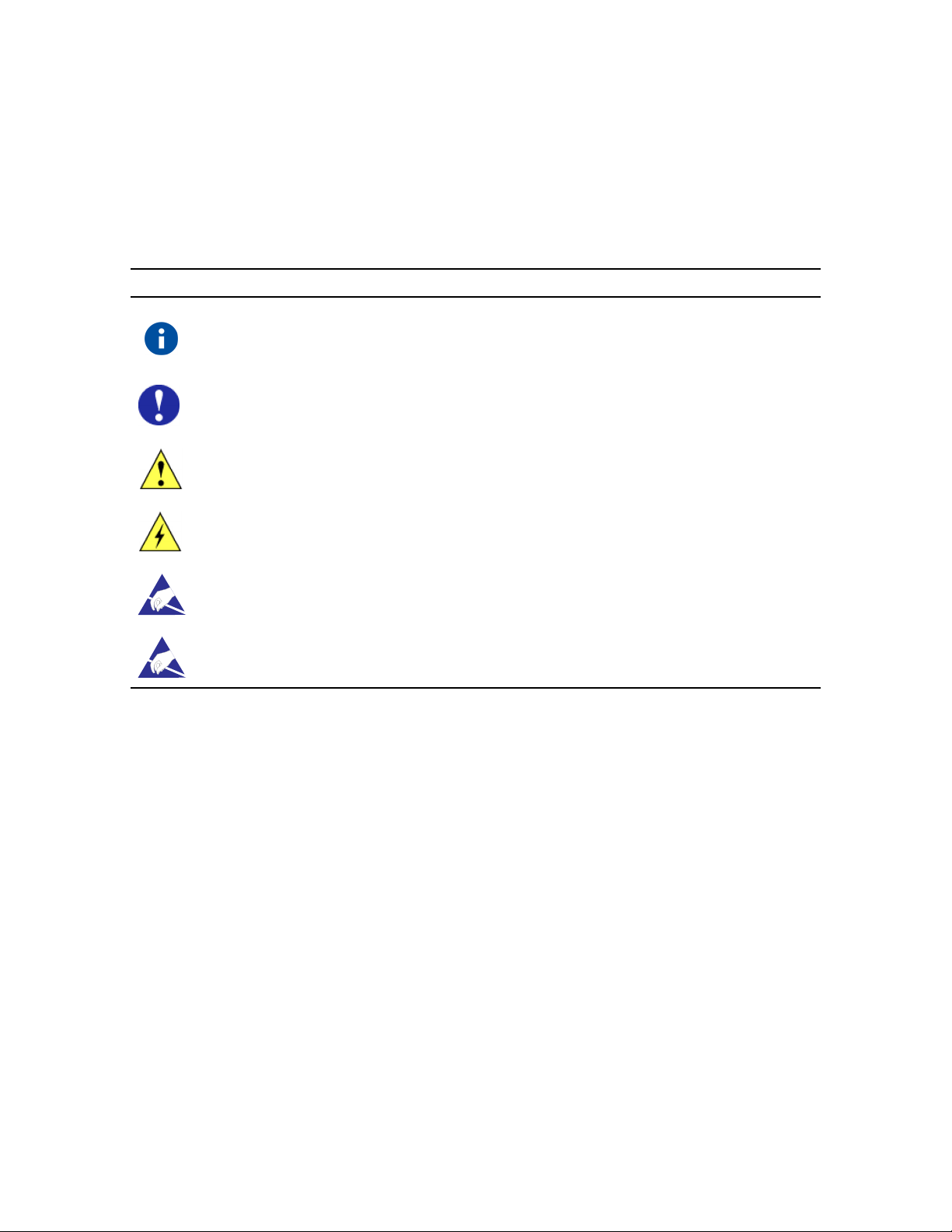
1.4 Text Convention
The following table shows the symbol conventions used in this manual for notification and
important instructions.
Icon Type Description
Note
Table 1 Symbol Conventions
Provides helpful suggestions needed in understanding
a feature or references to material not available in the
manual.
Alert
Caution
Warning
Electro-Static Discharge
(ESD)
Danger
All dates are in ISO 8601 format, i.e. YYYY-MM-DD
PRELIMINAR
1.5 Related Documents
Please refer to http://www.telit.com/gnss/ for current documentation and downloads.
Alerts you of potential damage to a program, device,
or system or the loss of data or service.
Cautions you about a situation that could result in
minor or moderate bodily injury if not avoided.
Y
Warns you of a potential situation that could result in
death or serious bodily injury if not avoided.
Notifies you to take proper grounding precautions
before handling a product.
Indicates information MUST be followed or
catastrophic equipment failure or bodily injury may
occur
1.5.1 Related Documents and Download
– Datasheets
– Product User Guides
– EVK User Guides
– Software User Guides
– Application Notes
– TelitView installation and documentation
1VV0301487 Rev. 1.2 8 2018-07-27
Page 9

WE866E4-P Module Hardware User Guide
1.5.2 Related Documents requiring a Non Disclosure Agreement
– Authorized Software User Guides
– Product firmware
Y
PRELIMINAR
1VV0301487 Rev. 1.2 9 2018-07-27
Page 10

WE866E4-P Module Hardware User Guide
Y
PRELIMINAR
1VV0301487 Rev. 1.2 10 2018-07-27
Page 11

WE866E4-P Module Hardware User Guide
Chapter 2 Overview
The aim of this document is to describe some hardware solutions useful for developing a
product with Telit WE866E4-P module. All the basic functions of a mobile phone is
considered and certified for an appropriate hardware solution, common errors and wrong
solution that can be avoided are documented. The wrong solutions to be avoided shall be
considered as mandatory, while the suggested hardware configurations shall not be
considered mandatory, instead the information given shall be used as a guide and a starting
point for proper development of a product with the Telit WE866E4-P module.
For further hardware details refer to the “Telit WE866E4-P Product Description” document
where all the hardware information is reported.
NOTE:
1).(EN) The integration of WE866E4-P WiFi+BT module within user application
shall be done according to the design rules describe in this manual.
2).(IT)
3).(DE)
4).(SL)
5).(FR)
6).(HE)
Y
PRELIMINAR
1VV0301487 Rev. 1.2 11 2018-07-27
Page 12

WE866E4-P Module Hardware User Guide
Y
PRELIMINAR
1VV0301487 Rev. 1.2 12 2018-07-27
Page 13

WE866E4-P Module Hardware User Guide
Chapter 3 Pin Allocation
• Pins Out, page 13
• A Pad Layout, page 16
3.1 Pins Out
Table 2, page 13 describes the WE866E4-P module pin signal description.
Table 2 WE866E4-P Module Pin Signal Description
Pins Name Input/Output Function Type Comments
USB HS 2.0 COMMUNICATION PORT
E5 USB_D+ Input/Output USB differential Data+
E6 USB_D- Input/Output USB differential Data -
E4 VUSB Input Power sense for USB
High Speed Asynchronous Serial Port (USIF0)
A4 UART0_TXD Output Serial data output
A5 UART0_RXD Input Serial data input CMOS VIO
B4 UART0_RTS Output Output CMOS VIO
B3 UART0_CTS Input Input CMOS VIO
Low Speed Asynchronous Serial Port (USIF0)
C3 UART1_RXD Input Serial data input CMOS VIO
C4 UART1_TXD Output Serial data input CMOS VIO
Serial Peripheral Interface (SPI) CMOS VIO
A3 SPI_MISO Input Pull-down (see Note 1) CMOS VIO Master
B2 SPI_MOSI Output Pull-down (see Note 1) CMOS VIO Master
A2 SPI_CLK Output Pull-down (see Note 1) CMOS VIO Master
D9 SPI_CS Output Pull-down CMOS VIO Master
Secure Digital Input Output (SDIO)
A6 SDIO_D2 Input/Output DATA2 CMOS VIO
PRELIMINAR
Y
CMOS VIO
B6 SDIO_D1 Input/Output DATA1 CMOS VIO
B7 SDIO_D3 Input/Output DATA3 CMOS VIO
C7 SDIO_D0 Input/Output DATA0 CMOS VIO
D7 SDIO_CLK Input/Output Clock CMOS VIO
E7 SDIO_CMD Input/Output Command CMOS VIO
Inter - Integrated Circuit Interface
1VV0301487 Rev. 1.2 13 2018-07-27
Page 14

WE866E4-P Module Hardware User Guide
Table 2 WE866E4-P Module Pin Signal Description (Continued)
Pins Name Input/Output Function Type Comments
F8 I2C_SDA Input/Output Data CMOS VIO
G8 I2C_SCL Input/Output Clock CMOS VIO GPIO_7
Analog Interface
A8 ADC_IN1 Input 12 BITS 1Mhz VIO 1V8 only
A9 ADC_IN2 Input 12 BITS 1Mhz VIO 1V8 only
B9 ADC_IN3 Input 12 BITS 1Mhz VIO 1V8 only
Digital Audio Interface (I2S) Master/Slave
C5 I2S_SYNC Input/Output Synchronization CMOS VIO
D5 I2S_SCK Input/Output Clock CMOS VIO
C6 I2S_SDI Input Input Data CMOS VIO
D6 I2S_SDO Output Output Data CMOS VIO
GP
IO_6
Miscellaneous Functions
G5 WiFI_EN Input Power Enable CMOS VIO Active HI
G6 BT_EN Input Power Enable CMOS VIO Active HI
D1 ANT_1 Input/Output Wi-Fi 2.4G and 5G RF 50Ohms
G3 ANT_2 Input/Output BT 2.4G CMOS VIO 50Ohms
D3 GPIO_1 Input/Output GENERIC IO CMOS VIO WAKEUP
E3 GPIO_2 Input/Output GENERIC IO CMOS VIO BT_PRIORITY
F5 GPIO_3 Input/Output GENERIC IO CMOS VIO WI-FI ACTIVE
F6 GPIO_4 Input/Output GENERIC IO CMOS VIO BT_ACTIVE
F7 GPIO_5 Input/Output GENERIC IO CMOS VIO DAC_OUT
Power Supply
A1 VDD_BLE Input Main BLE Power Supply Power
A2 VDD_WLAN Input Main Wi-Fi Power Supply Power
A3 VIO Input Digital I/O Power Supply Power
B1 GND Ground Power
B2 GND Ground Power
C1 GND Ground Power
C2 GND Ground Power
PRELIMINAR
Y
D2 GND Ground Power
E1 GND Ground Power
E2 GND Ground Power
F1 GND Ground Power
F2 GND Ground Power
F3 GND Ground Power
1VV0301487 Rev. 1.2 14 2018-07-27
Page 15

WE866E4-P Module Hardware User Guide
Table 2 WE866E4-P Module Pin Signal Description (Continued)
Pins Name Input/Output Function Type Comments
F4 GND Ground Power
G1 GND Ground Power
G2 GND Ground Power
G4 GND Ground Power
G7 GND Ground Power
A7 GND Ground Power
C9 GND Ground Power
Reversed
B5 RESERVED RESERVED
D4 RESERVED RESERVED
Y
PRELIMINAR
1VV0301487 Rev. 1.2 15 2018-07-27
Page 16

WE866E4-P Module Hardware User Guide
3.2 A Pad Layout
The following representation shows the top view of the Pad layout:
ABCDEFG
1 VDD_BLE GND GND ANT_1 GND GND GND
2 VDD_WLAN GND GND GND GND GND GND
3 VIO UART0_CTS UART1_RX
4 UART0_TXD UART0_RTS UART_TX RES USB_VDD GND GND
5 UART0_RX RES I2S_SYNC I2S_SCK USB_DP
6 SDIO_D2 SDIO_D1 I2S_SDI I2S_SDO USB_DM
SDIO_D3
7 GND
8 ADC_IN1 JTAG_TCK JTAG_TD0 JTAG_TMS JTAG_TDI
SPI_MOSI
UART0_RTS
SDIO_D0
SPI_MISO
UART0_RXD
GPIO_1
WAKEUP
SDIO_CLK
SPI_CLK
UART0_CTS
GPIO_2
BT_PRIORITY
Y
SDIO_CMD
SPI_CS
UART0_TXD
GND ANT_2
GPIO_3
Wi-Fi Active
GPIO_4
BT_ACTIVE
GPIO_5
DAC_OUT1
GPIO_6
I2C_SDA
WiFi_EN
BT_EN
GPIO_7
I2C_SCL
GND
9 ADC_IN2 ADC_IN3 GND
PRELIMINAR
SPI_CS
(MASTER)
GPIO
SPI_CLK
(MASTER)
GPIO
SPI_MOSI
(MASTER)
GPIO
SPI_MISO
(MASTER)
GPIO
1VV0301487 Rev. 1.2 16 2018-07-27
Page 17
WE866E4-P Module Hardware User Guide
Chapter 4 Power Supply
• Power Supply Requirements, page 17
• Power Consumption, page 17
• General Design Rules, page 18
4.1 Power Supply Requirements
Table 3, page 17 provide the Power supply requirements of WE866E4-P module.
Power Supply Minimum Typical Maximum
Table 3 Power Supply Requirements
Absolute Maximum to avoid
permanent damage at any power supply
pin
Recommended-VDD_BLE,
VDD_WLAN, USB_VDD
Recommended VIO 3.14/1.71V 3.3V/1.8V 3.46V/1.86V
Note: The ADC cannot be used if VIO is not equal to 1V8.
4.2 Power Consumption
PRELIMINAR
Table 4, page 17 lists the types of Power Consumption.
Y
-0.3V 4.0V
3.14V 3.3V 3.46V
Table 4 Power Consumption
Power Consumption Typical
POWER DOWN WiFi_EN=0, BT_EN=0 TBD μA
Suspend TBD μA
Host OFF TBD μA
Sleep TBD μA
ON; Radio OFF TBD mA
BLE RX TBD mA
BLE TX TBD mA
WiFi RX TBD mA
WiFi TX TBD mA
1VV0301487 Rev. 1.2 17 2018-07-27
Page 18

WE866E4-P Module Hardware User Guide
DTIM=1 TBD mA
DTIM=3 TBD μA
DTIM=10 TBD μA
4.3 General Design Rules
It is recommended to provide a 10μF capacitors right next to the VDD_WLAN and BT
pins, and 2.2μF at each of the other power supply pins like VIO.
Table 4 Power Consumption
Power Consumption Typical
Y
PRELIMINAR
1VV0301487 Rev. 1.2 18 2018-07-27
Page 19

WE866E4-P Module Hardware User Guide
Chapter 5 Digital Section
• Logic Levels, page 19
• Power Up/Down Sequence, page 20
• Power ON Reset Time, page 20
• Unconditional Shutdown, page 20
• Communication Ports, page 21
• General Purpose Input/Output, page 22
5.1 Logic Levels
Table 5, page 19 describes the logic level of the voltage between signal and ground.
Table 5 Logic Level
Parameter Minimum Maximum
Input level on any digital pin -0.3V VIO + 0.3V
Levels with VIO = 3.3V
Input high level 2.4V 3.6V
V
IH
Input low level -0.3V 0.3V
V
IL
Output high level 3.0V 3.6V
V
OH
Output high level -0.3V 0.4V
V
PRELIMINAR
OL
Levels with VIO = 3.3.V Typical
Input current
I
IH
I
Input current
IL
I
Output current
OH
60 μA (Rod is ON)
0.1 μA (Rpd is OFF)
60 μA (Rod is ON)
0.1 μA (Rpd is OFF)
5mA (x4 drive strength)
3.3mA (x2 drive strength)
2.6(x1 drive strength)
Y
5mA (x4 drive strength)
I
Output current
OL
Note: The ADC cannot be used if VIO is not equal to 1V8.
1VV0301487 Rev. 1.2 19 2018-07-27
3.3mA (x2 drive strength)
2.6(x1 drive strength)
Page 20

WE866E4-P Module Hardware User Guide
5.2 Power Up/Down Sequence
The BT_EN is the main power enable pin including the WIFI_EN. All supplies should be
stable for a minimum of 10 μs before BT_EN is de-asserted (i.e, greater than VIL for
VIO). If VIO = 3.3V, then VDD_BLE, VDD_WLAN, and VIO shares the same 3.3V power
(see Figure 1, page 20).
Figure 1 Power Up/Down Sequence
PRELIMINAR
5.3 Power ON Reset Time
Table 6, page 20 describes the Power ON reset time.
Parameter Description Minimum Maximum Units
tR
tS
Rise time of poweer to 90% of final
voltage
Minimum of 10 uS before BLE_EN is
asserted
Y
Table 6 Power ON Reset Time
N/A 25 ms
10 N/A μs
5.4 Unconditional Shutdown
The BT_EN is used for unconditional shutdown.
1VV0301487 Rev. 1.2 䢴䢲 2018-07-27
Page 21

WE866E4-P Module Hardware User Guide
5.5 Communication Ports
5.5.1 High Speed UART
High-speed Universal Asynchronous Receiver/Transmitter (UART) interfaces is
configured to serve either as a host interface link or a debug message console.
Two HS UART interfaces are present, one with dedicated pin out and second sharing the
pins with the SDIO interface pins.
Table 7, page 21 describes the High Speed UART Configuration for WE866E4-P.
Property Configuration
Table 7 High Speed UART Configuration
5.5.2 Low Speed UART
High-speed Universal Asynchronous Receiver/Transmitter (UART) interfaces is
PRELIMINAR
configured to serve either as debug port.
Table 8, page 21 describes the Low Speed UART Configuration for WE866E4-P.
Baudrate
Data Bits 8-Bits
Flow Control CTS/RTS
Parity None
Stop Bits 1
Bit Order LS Bit First
Property Configuration
Baudrate Up to 115200 bps, no auto-baud rate detection, debug port
115200 bps, no auto-baud rate detection, can be changed by the
host up to 3 Mbps using a special command
Y
Table 8 Low Speed UART Configuration
Data Bits 8-Bits
Flow Control CTS/RTS
Parity None
Stop Bits 1
Bit Order LS Bit First
1VV0301487 Rev. 1.2 21 2018-07-27
Page 22

WE866E4-P Module Hardware User Guide
5.5.3 SDIO
One SDIO Slave interface.
– Compliant to SDIO v2.0 specification
– Interface clock frequency up to 48 MHz
– Data transfer modes: 4-bit SDIO, 1-bit SDIO, SPI
5.5.4 SPI
The two general-purpose SPI interfaces are one configured as dedicated master and the
other configured as master/slave pin-mux with SDIO interface pins.
– Interface clock frequency up to 48 MHz
5.5.5 I2C
The I2C Master/Salve interface have weak internal processing unit. So add external
processing unit of 4.7K down to 1K, if needed.
5.5.6 USB
USB 2.0 device interface, provide a simplified, high-speed and scalable manufacturing test
and configuration for QCA4020-based systems.
5.6 General Purpose Input/Output
PRELIMINAR
It is a special signaling GPIO.
5.6.1 ADC Converter
Analog to Digital Converter (ADC) measurements for inputs:
– 12-bit ADC up to 1Msps
– Alternatively 1 differential input, -1.75V to +1.75V, common mode 0.875V
Y
1VV0301487 Rev. 1.2 䢴䢴 2018-07-27
Page 23

WE866E4-P Module Hardware User Guide
Chapter 6 RF Section
• RF Variants, page 23
• TX Output Power, page 24
• RX Sensitivity, page 26
• Wi-Fi Antenna Requirements, page 27
• BlueTooth Antenna Requirements, page 29
6.1 RF Variants
6.1.1 Wi-Fi
6.1.2 Bluetooth
Y
Table 9, page 23 describes the Wi-Fi RF Frequency band.
Table 9 Wi-Fi Frequency Band
RF Frequency Channel Range Units
2.4GHz RF Frequency range
5GHz RF Frequency range
Center channel frequency
at 5MHz spacing
Center channel frequency
at 5MHz spacing
2.412 ≤ Fc ≤
2.484
4.9 ≤ Fc ≤ 5.925 GHz
PRELIMINAR
Table 10, page 23 describes the Bluetooth RF Frequency band.
Table 10 Wi-Fi Frequency Band
RF Frequency Channel Range Units
RF Frequency range
Fc=2402 + k × 2 MHz,
where k = 0, ..., 39
2.4 ≤ F ≤ 2.4835. GHz
GHz
1VV0301487 Rev. 1.2 23 2018-07-27
Page 24

WE866E4-P Module Hardware User Guide
6.2 TX Output Power
6.2.1 Wi-Fi
6.2.1.1 For 2.4GHz
Table 11, page 24 lists the Wi-Fi RF Frequency Transmission for 2.4GHz.
Table 11 Wi-Fi RF Frequency Transmission for 2.4GHZ
Standard Modulation Data rates
Index
BPSK 1 Mbps 19 NA NA dBm
802.11b
802.11g
QPSK 2 Mbps 19 NA NA dBm
CCK 5.5 Mbps 19 NA NA dBm
CCK 11 Mbps 19 NA NA dBm
BPSK 6 Mbps 19 NA NA dBm
BPSK 9 Mbps 19 NA NA dBm
QPSK 12 Mbps 19 NA NA dBm
QPSK 18 Mbps 18 NA NA dBm
16 QAM 24 Mbps 18 NA NA dBm
16 QAM 36 Mbps 18 NA NA dBm
64 QAM 48 Mbps 18 NA NA dBm
64 QAM 54 Mbps 18 NA NA dBm
BPSK MCS0 NA 19 18 dBm
QPSK MCS1 NA 19 18 dBm
PRELIMINAR
2.4 GHz: Transmit power with IEEE 802.11 EVM and spectral mask
compliance at balun output at 25 °
802.11b/g 802.11n 20 MHz 802.11n 40 MHz Unit
Typ Typ Ty p
Y
QPSK MCS2 NA 19 18 dBm
802.11n
Note: The performance includes balun, but excludes external duplexer, filter and external switch loss.
1VV0301487 Rev. 1.2 24 2018-07-27
16 QAM MCS3 NA 18 18 dBm
16 QAM MCS4 NA 18 18 dBm
64 QAM MCS5 NA 17 17 dBm
64 QAM MCS6 NA 17 17 dBm
64 QAM MCS7 NA 17 17 dBm
Page 25

WE866E4-P Module Hardware User Guide
6.2.1.2 For 5GHz
Table 12, page 25 lists the Wi-Fi RF Frequency Transmission for 5GHz.
Table 12 Wi-Fi RF Frequency Transmission for 5GHZ
Standard Modulation Data rates
Index
BPSK 6 Mbps 16 NA NA dBm
BPSK 9 Mbps 16 NA NA dBm
QPSK 12 Mbps 16 NA NA dBm
QPSK 18 Mbps 16 NA NA dBm
802.11b
16 QAM 24 Mbps 16 NA NA dBm
16 QAM 36 Mbps 14 NA NA dBm
64 QAM 48 Mbps 13 NA NA dBm
64 QAM 54 Mbps 13 NA NA dBm
BPSK 6 Mbps 19 NA NA dBm
BPSK 9 Mbps 19 NA NA dBm
QPSK 12 Mbps 19 NA NA dBm
QPSK 18 Mbps 18 NA NA dBm
802.11g
16 QAM 24 Mbps 18 NA NA dBm
16 QAM 36 Mbps 18 NA NA dBm
2.4 GHz: Transmit power with IEEE 802.11 EVM and spectral mask
compliance at balun output at 25 ° Degrees
802.11b/g 802.11n 20 MHz 802.11n 40 MHz Unit
Typ Ty p Typ
Y
64 QAM 48 Mbps 18 NA NA dBm
64 QAM 54 Mbps 18 NA NA dBm
BPSK MCS0 NA 16 15 dBm
QPSK MCS1 NA 16 15 dBm
QPSK MCS2 NA 15 14 dBm
16 QAM MCS3 NA 15 14 dBm
802.11n
16 QAM MCS4 NA 14 13 dBm
64 QAM MCS5 NA 14 13 dBm
64 QAM MCS6 NA 13 12 dBm
64 QAM MCS7 NA 13 12 dBm
Note: The performance includes balun, but excludes external duplexer, filter and external switch loss.
PRELIMINAR
1VV0301487 Rev. 1.2 25 2018-07-27
Page 26

WE866E4-P Module Hardware User Guide
6.2.2 Bluetooth
Table 13, page 26 lists the Bluetooth Transmission.
TX Characteristic Rate Min Type Max Units
Table 13 Bluetooth Transmission
Max RF Output Power
LE 1M 1.5 4 4.3 dBm
LE 2M 1.5 4 4.2 dBm
Note:
1).Measurement data is at chip output, 25°C, 1.8V IO. 2).When Tx power higher than 4dBm, an external BPF is required for out of band emission. BPF spec is upon the external PA is selected.
6.3 RX Sensitivity
6.3.1 Wi-Fi
6.3.1.1 For 2.4GHz
Table 14, page 26 lists the RX Sensitivity for 2.4GHz.
Table 14 RX Sensitivity for 2.4GHZ
Standard Modulation Data rates
Index
PRELIMINAR
BPSK 1 Mbps 19 NA NA dBm
Y
2.4 GHz: Transmit power with IEEE 802.11 EVM and spectral mask
compliance at balun output at 25 °Degrees
802.11b/g 802.11n 20 MHz 802.11n 40 MHz Unit
Typ Typ Ty p
802.11b
802.11g
Note: The performance includes balun, but excludes external duplexer, filter and external switch loss.
6.3.1.2 For 5GHz
1VV0301487 Rev. 1.2 26 2018-07-27
QPSK 2 Mbps 19 NA NA dBm
CCK 5.5 Mbps 19 NA NA dBm
CCK 11 Mbps 19 NA NA dBm
BPSK 6 Mbps 19 NA NA dBm
BPSK 9 Mbps 19 NA NA dBm
Table 15, page 27 lists the RX Sensitivity for 5GHz.
Page 27

WE866E4-P Module Hardware User Guide
Table 15 RX Sensitivity for 5GHZ
Standard Modulation Data rates
Index
BPSK 6 Mbps -93 NA NA dBm
802.11b
64 QAM 54 Mbps -75.5 NA NA dBm
BPSK MCS0 NA -93 -90 dBm
802.11g
64 QAM MCS7 NA -72.5 -69 dBm
Note: The performance includes balun, but excludes external duplexer, filter and external switch loss.
6.3.2 Bluetooth
Table 16, page 27 lists the Bluetooth RX Sensitivity.
Table 16 Bluetooth RX Sensitivity
RX Characteristic Rate Min Type Max Units
RX Sensitivity 1Mbps <-= -70dBM -97 -99 dBm
Note: Measurement data is at chip output, 25°C, 1.8V IO.
2.4 GHz: Transmit power with IEEE 802.11 EVM and spectral mask
802.11b/g 802.11n 20 MHz 802.11n 40 MHz Unit
Typ Typ Ty p
compliance at balun output at 25 °
Y
6.4 Wi-Fi Antenna Requirements
Special care must be taken during the design of the RF section on the application board.
PRELIMINAR
CAUTION! : If The below recommendation is strictly not followed then RF performance
degradation and infringements of emission limits will occur
A 50Ω antenna is required with Telit’s WE866E4-P module interface features an SMA
connector for an external antenna, alternatively a chip or a printed antenna can be used.
If an integrated or printed antenna is used, it is recommended to place it at the edge of the
application board. Since the antenna impedance is required to be tuned to 50Ω.
It is recommended to foresee a PI matching network between the WE866E4-P module and
the antenna during first prototyping. If not, a series 0Ω-resistor can be used, leaving the two
shunt components unpopulated.
To meet Telit’s FCC certification standard, the antenna on the application board should
have a gain value equal/less then the one recommended by Telit.
1VV0301487 Rev. 1.2 27 2018-07-27
Page 28

WE866E4-P Module Hardware User Guide
6.4.1 PCB Design Guidelines
The WE866E4-P module provides a 50Ω antenna pad, which is routed to the antenna
connector (or the integrated antenna) by means of a transmission line.
It is important that the impedance of this line is controlled to 50Ω. The line should be as
short as possible with a constant cross section and without abrupt curves. It is isolated from
any other noise sources and cross overs from other lines in adjacent layers. Instead, a
continuous ground plane is recommended under the antenna trace and a ground via curtain
should connect to the coplanar ground planes.
An example of implementation - the details of the antenna trace on the WE866E4-P
interface board is as described:
A Grounded Coplanar Waveguide (G-CPW) line has been chosen, since this kind of
transmission line ensures good impedance control and can be implemented in an outer PCB
layer as required in this case. A SMA female connector has been used to feed the line.
The interface board is realized on a FR4, 4-layers PCB. Substrate material is characterized
by relative permittivity εr = 4.6 ± 0.4 @ 1 GHz, TanD= 0.019 ÷ 0.026 @ 1 GHz.
A characteristic impedance of nearly 50 Ω is achieved using trace width of 1.1 mm,
clearance from coplanar ground plane = 0.3 mm each side. The line uses reference ground
plane on layer 3, while copper is removed from layer 2 underneath the line. Height of the
trace above ground plane is 1.335 mm. Calculated characteristic impedance is 51.6 Ω,
estimated line loss is less than 0.1 dB.
Figure 2, page 28 shows the line geometry:
Figure 2 PCB Design
Y
PRELIMINAR
1VV0301487 Rev. 1.2 28 2018-07-27
Page 29

WE866E4-P Module Hardware User Guide
6.4.2 PCB Guidelines in case of FCC Certification
TBD
6.5 BlueTooth Antenna Requirements
6.5.1 PCB Design Guidelines
TBD
6.5.2 PCB Guidelines in case of FCC Certification
TBD
Y
PRELIMINAR
1VV0301487 Rev. 1.2 29 2018-07-27
Page 30

WE866E4-P Module Hardware User Guide
Y
PRELIMINAR
1VV0301487 Rev. 1.2 30 2018-07-27
Page 31

WE866E4-P Module Hardware User Guide
Chapter 7 Audio Section
• Electrical Characteristics, page 31
• Codec Examples, page 31
7.1 Electrical Characteristics
The audio interface is only digital, through the I2S.The voltage of this interface pins have
same electrical characteristics as for digital pins and are related to the power bank VIO.
7.2 Codec Examples
TBD
Y
PRELIMINAR
1VV0301487 Rev. 1.2 31 2018-07-27
Page 32

WE866E4-P Module Hardware User Guide
Y
PRELIMINAR
1VV0301487 Rev. 1.2 32 2018-07-27
Page 33

WE866E4-P Module Hardware User Guide
Chapter 8 Mechanical Design
• Drawing, page 33
8.1 Drawing
Figure 3, page 33 shows the Mechanical Design of the module.
Figure 3 Mechanical Design
Y
PRELIMINAR
1VV0301487 Rev. 1.2 33 2018-07-27
Page 34

WE866E4-P Module Hardware User Guide
Figure 4, page 34 shows the Top View of WE866E4-P module.
Figure 4 Top View of WE866E4-P Module
Y
PRELIMINAR
1VV0301487 Rev. 1.2 34 2018-07-27
Page 35

WE866E4-P Module Hardware User Guide
Chapter 9 Application PCB Design.
• Footprint, page 35
• PCB Pad Design, page 37
• PCB Pad Dimension, page 38
• Stencil, page 39
• Solder Paste, page 39
• Solder Re-flow, page 39
9.1 Footprint
Figure 5, page 35 shows the top view Footprint of copper pad pattern.
Figure 5 Copper pad Pattern - Top View
Y
PRELIMINAR
1VV0301487 Rev. 1.2 35 2018-07-27
Page 36

WE866E4-P Module Hardware User Guide
Figure 6, page 36 shows the Pad A details.
Figure 6 Pad A Details
Y
Figure 7, page 36 shows the Pad details.
Figure 7 Pad Details
PRELIMINAR
1VV0301487 Rev. 1.2 36 2018-07-27
Page 37

WE866E4-P Module Hardware User Guide
Figure 8, page 37 shows the top view of Solder resist pattern.
Figure 8 Solder Resist Pattern-Top View
PRELIMINAR
9.2 PCB Pad Design
Non-Solder Mask Defined (NSMD) type is recommended for the solder pads on the PCB.
Figure 9, page 38 shows the PCB pad design.
Y
1VV0301487 Rev. 1.2 37 2018-07-27
Page 38

WE866E4-P Module Hardware User Guide
Figure 9 Solder Pads on PCB
9.3 PCB Pad Dimension
It is not recommended to place or micro-via not covered by solder resist in an area of 0.3
mm around the pads unless it carries the same signal of the pad itself. Holes in the pad are
allowed only for blind holes and not for through holes. Figure 10, page 38 shows the Pad
dimension:
PRELIMINAR
Figure 10 Solder Resist Pattern-Top View
Y
1VV0301487 Rev. 1.2 38 2018-07-27
Page 39

WE866E4-P Module Hardware User Guide
9.3.1 Recommendations for PCB Pad Surface
Table 17, page 39 provides the recommendation for PCB Pad Surface.
Table 17 Recommendation for PCB Pad Surface
9.4 Stencil
9.5 Solder Paste
Finish Layer Thickness
(um)
Electro-less
Ni/Immersion Au
The PCB must be able to resist higher temperatures which occurs at the lead-free process.
This issue should be discussed with the PCB supplier. Generally, the wettability of tin-lead
solder paste on the described surface plating is better compared to lead-free solder paste.
It is not necessary to panel the application PCB, however it is suggested to use milled
contours and pre-drilled board breakouts. Scoring or v-cut solutions are not recommended.
3 - 7/ 0.03 - 0.15
Good solderability
protection, high shear force
values
Properties
Y
Stencil’s apertures layout can be the same of the recommended footprint (1:1), a thickness
of stencil foil ≥ 120 μm is suggested.
It is recommended to use only “no clean” solder paste in order to avoid the cleaning of the
modules after assembly. The lead-free solder paste is Sn/Ag/Cu.
PRELIMINAR
9.6 Solder Re-flow
Figure 11, page 40 shows the recommended solder profile re-flow:
1VV0301487 Rev. 1.2 39 2018-07-27
Page 40

WE866E4-P Module Hardware User Guide
Figure 11 Solder Re-flow Profile
Y
Table 18, page 40 provides the Solder re-flow profile features and its Pb-Free Assembly.
Table 18 Solder Re-flow Parameters
Profile Features Pb-Free Assembly
Average ramp-up rate (TL to TP) 3°C/second max
Preheat
Temperature Min (Tsmin) 150°C
PRELIMINAR
Temperature Max (Tsmax) 200°C
Time (min to max) (ts) 60-180 seconds
Tsmax to TL
Ramp-up rate 3°C/second max
Time Maintained
Temperature (TL) 217°C
Time (t) 60-150 seconds
Peak Temperature (Tp) 245 +0/-5°C
Time within 5°C of actual Peak
Temperature (tp)
10-30 seconds
Ramp-down Rate 6°C/second max
Time 25°C to Peak Temperature 8 minutes max
1VV0301487 Rev. 1.2 40 2018-07-27
Page 41

WE866E4-P Module Hardware User Guide
NOTE: All temperatures refer to topside of the package, measured on the package body
surface.
CAUTION! WE866E4 module withstands one re-flow process only.
Y
PRELIMINAR
1VV0301487 Rev. 1.2 41 2018-07-27
Page 42

WE866E4-P Module Hardware User Guide
Y
PRELIMINAR
1VV0301487 Rev. 1.2 42 2018-07-27
Page 43

WE866E4-P Module Hardware User Guide
Chapter 10 Packaging
• Tray, page 43
• Reel, page 44
• Moisture Sensitivity, page 46
10.1 Tray
The WE866E4-P modules are packaged in trays of 50 pieces each where small quantities
are required (i.e. for test and evaluation purposes). Trays are not designed to be used in
SMT processes for pick and place handling.
Figure 12 Packaging in Trays
Y
PRELIMINAR
1VV0301487 Rev. 1.2 43 2018-07-27
Page 44

WE866E4-P Module Hardware User Guide
10.2 Reel
Figure 13, page 44 shows WE866E4-P modules that are packaged on reels of 200 pieces
each.
Figure 13 Reel - Packaging
Y
PRELIMINAR
1VV0301487 Rev. 1.2 44 2018-07-27
Page 45

WE866E4-P Module Hardware User Guide
Figure 14, page 45 shows the schematic representation of Packaging.
Figure 14 Reel - Packaging in Trays
Y
PRELIMINAR
1VV0301487 Rev. 1.2 45 2018-07-27
Page 46

WE866E4-P Module Hardware User Guide
CAUTION! These trays can withstand a maximum temperature of 65°C.
10.3 Moisture Sensitivity
According to IPC/JEDEC J-STD-020 standards the moisture sensitivity level of the
WE866E4-P module Product is “3”. To use such a component the customer has to take care
of the following conditions:
a. The shelf life of the Product inside the dry bag is 12 months - from the seal date of
the bag, when stored in a non-condensing atmospheric environment of < 40°C and
< 90% RH.
b. Environmental condition during the production: <= 30°C / 60% RH according to
IPC/JEDEC J-STD-033B.
c. The maximum time between the opening of the sealed bag and the re-flow process
must be 168 hours if condition (b) “IPC/JEDEC J-STD-033B paragraph 5.2” is
followed.
Y
d. Baking is required if conditions (b) or (c) are not followed.
e. Baking is required if the humidity indicator inside the bag indicates 10% RH or
more.
PRELIMINAR
1VV0301487 Rev. 1.2 46 2018-07-27
Page 47

WE866E4-P Module Hardware User Guide
Chapter 11 Conformity Assessment Issue
• FCC/IC Regulatory Notice, page 47
11.1 FCC/IC Regulatory Notice
TBD
Y
PRELIMINAR
1VV0301487 Rev. 1.2 47 2018-07-27
Page 48

WE866E4-P Module Hardware User Guide
Y
PRELIMINAR
1VV0301487 Rev. 1.2 48 2018-07-27
Page 49

WE866E4-P Module Hardware User Guide
Chapter 12 Safety Recommendation
• Read Carefully, page 49
12.1 Read Carefully
Be sure the use of this product is allowed in the country and in the environment required.
The use of this product may be dangerous and has to be avoided in the following areas:
• Where it can interfere with other electronic devices in environments such as hospitals,
airports, aircrafts, etc.
• Where there is risk of explosion such as gasoline stations, oil refineries, etc. It is the
responsibility of the user to enforce the country regulation and the specific
environment regulation.
Do not disassemble the product; any mark of tampering will compromise the warranty
validity. We recommend following the instructions of the hardware user guides for correct
wiring of the product. The product has to be supplied with a stabilized voltage source and
the wiring has to be conformed to the security and fire prevention regulations. The product
has to be handled with care, avoiding any contact with the pins because electrostatic
discharges may damage the product itself. Same cautions have to be taken for the SIM,
checking carefully the instruction for its use. Do not insert or remove the SIM when the
product is in power saving mode.
Y
The system integrator is responsible for the functioning of the final product; therefore, care
has to be taken to the external components of the module, as well as any project or
installation issue, because the risk of disturbing the GSM network or external devices or
PRELIMINAR
having impact on the security. Should there be any doubt, please refer to the technical
documentation and the regulations in force. Every module has to be equipped with a proper
antenna with specific characteristics. The antenna has to be installed with care in order to
avoid any interference with other electronic devices and has to guarantee a minimum
distance from the body (20 cm). In case this requirement cannot be satisfied, the system
integrator has to assess the final product against the SAR regulation.
The European Community provides some Directives for the electronic equipment
introduced on the market. All of the relevant information is available on the European
Community website:
http://ec.europa.eu/enterprise/sectors/rtte/documents/
The text of the Directive 99/05 regarding telecommunication equipment is available, while
the applicable Directives (Low Voltage and EMC) are available at:
http://ec.europa.eu/enterprise/sectors/electrical/
1VV0301487 Rev. 1.2 49 2018-07-27
Page 50

WE866E4-P Module Hardware User Guide
Y
PRELIMINAR
1VV0301487 Rev. 1.2 50 2018-07-27
Page 51

WE866E4-P Module Hardware User Guide
Chapter 13 Acronyms
TTSC
USB
HS
DTE
UMTS
WCDMA
HSDPA
HSUPA
UART
HSIC
BLE
SPI
ADC
DAC
Telit Technical Support Centre
Universal Serial Bus
High Speed
Data Terminal Equipment
Universal Mobile Telecommunication System
Wide band Code Division Multiple Access
High Speed Downlink Packet Access
High Speed Uplink Packet Access
Universal Asynchronous Receiver Transmitter
High Speed Inter Chip
Bluetooth low energy
Serial Peripheral Interface
Analog – Digital Converter
Digital – Analog Converter
Y
I/O
PRELIMINAR
GPIO
CMOS
MOSI
MOSO
CLK
MRDY
SRDY
CS
RTC
PCB
ESR
VSWR
Input Output
General Purpose Input Output
Complementary Metal – Oxide Semiconductor
Master Output – Slave Input
Master Input – Slave Output
Clock
Master Ready
Slave Ready
Chip Select
Real Time Clock
Printed Circuit Board
Equivalent Series Resistance
Voltage Standing Wave Radio
1VV0301487 Rev. 1.2 51 2018-07-27
Page 52

WE866E4-P Module Hardware User Guide
VNA
Vector Network Analyzer
Y
PRELIMINAR
1VV0301487 Rev. 1.2 52 2018-07-27
Page 53

WE866E4-P Module Hardware User Guide
Document History
Revision Date Changes
0.0 January 2018 Initial Release.
1.0 March 2018
1.1 May 2018 Watermarked “PRELIMINARY”.
1.2 July 2018
Added Figure 4Top View of WE866E4-P
Module, page 34
Updates to Figure 3, page 33, Figure 4,
page 34
Y
PRELIMINAR
1VV0301487 Rev. 1.2 53 2018-07-27
Page 54

WE866E4-P Module Hardware User Guide
Y
PRELIMINAR
1VV0301487 Rev. 1.2 54 2018-07-27
Page 55

 Loading...