

Page 1

SL876Q5-A
Product User Guide
1VV0301333 Rev. 2
2017-06-27
Page 2

SL876Q5-A Product User Guide
SPECIFICATIONS ARE SUBJECT TO CHANGE WITHOUT NOTICE
NOTICE .
While reasonable efforts have been made to assure the accuracy of this document, Telit
assumes no liability resulting from any inaccuracies or omissions in this document, or from use
of the information obtained herein. The information in this document has been carefully
checked and is believed to be reliable. However, no responsibility is assumed for inaccuracies
or omissions. Telit reserves the right to make changes to any products described herein and
reserves the right to revise this document and to make changes from time to time in content
hereof with no obligation to notify any person of revisions or changes. Telit does not assume
any liability arising out of the application or use of any product, software, or circuit described
herein; neither does it convey license under its patent rights or the rights of others.
It is possible that this publication may contain references to, or information about Telit products
(machines and programs), programming, or services that are not announced in your country.
Such references or information must not be construed to mean that Telit intends to announce
such Telit products, programming, or services in your country.
COPYRIGHTS
This instruction manual and the Telit products described in this instruction manual may be,
include or describe copyrighted Telit material, such as computer programs stored in
semiconductor memories or other media. Laws in the Italy and other countries preserve for
Telit and its licensors certain exclusive rights for copyrighted material, including the exclusive
right to copy, reproduce in any form, distribute and make derivative works of the copyrighted
material. Accordingly, any copyrighted material of Telit and its licensors contained herein or in
the Telit products described in this instruction manual may not be copied, reproduced,
distributed, merged or modified in any manner without the express written permission of Telit.
Furthermore, the purchase of Telit products shall not be deemed to grant either directly or by
implication, estoppel, or otherwise, any license under the copyrights, patents or patent
applications of Telit, as arises by operation of law in the sale of a product.
COMPUTER SOFTWARE COPYRIGHTS
The Telit and 3rd Party supplied Software (SW) products described in this instruction manual
may include copyrighted Telit and other 3rd Party supplied computer programs stored in
semiconductor memories or other media. Laws in the Italy and other countries preserve for
Telit and other 3rd Party supplied SW certain exclusive rights for copyrighted computer
programs, including the exclusive right to copy or reproduce in any form the copyrighted
computer program. Accordingly, any copyrighted Telit or other 3rd Party supplied SW
computer programs contained in the Telit products described in this instruction manual may
not be copied (reverse engineered) or reproduced in any manner without the express written
permission of Telit or the 3rd Party SW supplier. Furthermore, the purchase of Telit products
shall not be deemed to grant either directly or by implication, estoppel, or otherwise, any
license under the copyrights, patents or patent applications of Telit or other 3rd Par ty suppl ied
SW, except for the normal non-exclusive, royalty free license to use that arises by operation
of law in the sale of a product.
1VV0301333 Rev. 2 Page 2 of 68 2017-06-27
Page 3

SL876Q5-A Product User Guide
USAGE AND DISCLOSURE RESTRICTIONS
I. License Agreements
The software described in this document is the property of Telit and its licensors. It is furnished
by express license agreement only and may be us ed only in accordance with the terms of such
an agreement.
II. Copyrighted Materials
Software and documentation are copyrighted materials. Making unauthorized copies is
prohibited by law. No part of the software or documentation may be reproduced, transmitted,
transcribed, stored in a retrieval system, or translated into any language or computer language,
in any form or by any means, without prior written permission of Telit
III. High Risk Materials
Components, units, or third-party products used in the product described herein are NOT faulttolerant and are NOT designed, manufactured, or i ntended for use as on-line control equipment
in the following hazardous environments requiring fail-safe controls: the operation of Nuclear
Facilities, Aircraft Navigation or Aircraft Communication Systems, Air Traffic Control, Life
Support, or Weapons Systems (High Risk Activities"). Telit and its supplier(s) specifically
disclaim any expressed or implied warranty of fitness for such High Risk Activities.
IV. Trademarks
TELIT and the Stylized T Logo are re gistered in Trademark Office. All other product or service
names are the property of their respective owners.
V. Third Party Rights
The software may include Third Party Right software. In this case you agree to comply w ith all
terms and conditions imposed on you in respect of such separate so ftware. In addition to Third
Party Terms, the disclaimer of warranty and limitation of liability provisions in this License shall
apply to the Third Party Right software.
TELIT HEREBY DISCLAIMS ANY AND ALL WARRANTIES EXPRESS OR I MPLIED FROM
ANY THIRD PARTIES REGARDING ANY SEPARATE FILES, ANY THIRD PARTY
MATERIALS INCLUDED IN THE SOFTWARE, ANY THIRD PARTY MATERIALS FROM
WHICH THE SOFTWARE IS DERIVED (COLLECTI VELY “OTHER CODE”), AND THE USE
OF ANY OR ALL THE OTHER CODE IN CONNECTION WITH THE SOFTWARE,
INCLUDING (WITHOUT LIMITATION) ANY WARRANTIES OF SATISFACTO RY QUALITY
OR FITNESS FOR A PARTICULAR PURPOSE.
NO THIRD PARTY LICENSORS OF OTHER CODE SHALL HAVE ANY LIABILITY FOR ANY
DIRECT, INDIRECT, INCIDENTAL, SPECIAL, EXEMPLARY, OR CONSEQUENTIAL
DAMAGES (INCLUDING WITHOUT LIMITATION LOST PROFITS), HOWEVER CAUSED
AND WHETHER MADE UNDER CONTRACT, TORT OR OTHER LEGAL THEORY, ARISING
IN ANY WAY OUT OF THE USE OR DISTRIBUTION OF THE OTHER CODE OR THE
EXERCISE OF ANY RIGHTS GRANTED UNDER EITHER O R BOTH THIS LICENSE AND
THE LEGAL TERMS APPLICABLE TO ANY SEPARATE FILES, EVEN IF ADVISED OF THE
POSSIBILITY OF SUCH DAMAGES.
1VV0301333 Rev. 2 Page 3 of 68 2017-06-27
Page 4

SL876Q5-A Product User Guide
Product
PRODUCT APPLICABILITY TABLE
SE876Q5-A
1VV0301333 Rev. 2 Page 4 of 68 2017-06-27
Page 5

SL876Q5-A Product User Guide
CONTENTS
NOTICE . .................................................................................................... 2
COPYRIGHTS ................................................................................................ 2
COMPUTER SOFTWARE COPYRIGHTS ...................................................... 2
USAGE AND DISCLOSURE RESTRICTIONS ............................................... 3
PRODUCT APPLICABILITY TABLE .............................................................. 4
1. INTRODUCTION ........................................................................ 11
Purpose ...................................................................................... 11
Contact and Support Information ................................................ 11
Text Conventions ........................................................................ 12
Related Documents .................................................................... 13
Related Documents Requiring a Non-disclosure Agreement ....... 13
2. PRODUCT DESCRIPTION ......................................................... 14
Product Overview ....................................................................... 14
SL876Q5-A Block Diagram ......................................................... 15
SL876Q5-A Module .................................................................... 16
3. SL876Q5-A EVALUATION KIT (EVK) ....................................... 17
SL876Q5-A Evaluation Board (EVB) ........................................... 18
4. PRODUCT FEATURES .............................................................. 19
Built-in Antenna and Switch ........................................................ 19
Multi-Constellation Navigation ..................................................... 19
Quasi-Zenith Satellite System (QZSS) support ........................... 19
Satellite Based Augmentation System (SBAS) ............................ 19
SBAS Corrections ....................................................................... 19
SBAS Ranging ............................................................................ 19
Assisted GPS (AGPS) - SiRFInstantFix™ ................................... 19
Client-generated Extended Ephemeris (CGEE) .......................... 20
Server-generated Extended Ephemeris (SGEE) ......................... 20
2-D Positioning ........................................................................... 20
Static Navigation ......................................................................... 20
Velocity Dead-Reckoning ............................................................ 21
Jamming Rejection – Continuous Wave (CW) Jamming Mitigation21
Elevation Mask Angle ................................................................. 21
5 Hz Navigation .......................................................................... 21
10 Hz Navigation ........................................................................ 22
1VV0301333 Rev. 2 Page 5 of 68 2017-06-27
Page 6
SL876Q5-A Product User Guide
1PPS .......................................................................................... 22
I/O Communication Ports ............................................................ 22
Power Management .................................................................... 23
Full Power Mode ......................................................................... 23
SmartGNSS ................................................................................ 23
Trickle Power .............................................................................. 24
Push-to-Fix ................................................................................. 24
SiRFaware .................................................................................. 24
Hibernate .................................................................................... 24
Internal LNA ................................................................................ 25
Device Wake-up (1st port) ........................................................... 25
MEMS Wakeup (2nd Port - I2C).................................................. 25
Host I/O Ports ............................................................................. 25
5. PRODUCT PERFORMANCE ..................................................... 26
Horizontal Position Accuracy ...................................................... 26
Time to First Fix .......................................................................... 26
Sensitivity ................................................................................... 27
6. SOFTWARE INTERFACE .......................................................... 28
NMEA Output Messages ............................................................ 28
Standard Messages .................................................................... 28
SiRF Proprietary Messages ........................................................ 29
Telit Proprietary Messages ......................................................... 29
NMEA Input Commands ............................................................. 30
Change output sentences and their rates .................................... 30
Change data rate ........................................................................ 30
Switch to OSP protocol ............................................................... 30
OSP Output Messages ............................................................... 30
OSP Input Commands ................................................................ 30
Change output messages ........................................................... 30
Change data rate ........................................................................ 30
Switch to NMEA protocol and data rate....................................... 30
7. FLASH UPG RADABI LI TY .......................................................... 31
8. ELECTRICAL INTERFACE ........................................................ 32
Module Pin-out ............................................................................ 32
DC Characteristics ...................................................................... 35
Absolute Maximum Ratings ........................................................ 35
Power Supply.............................................................................. 36
1.8 V Supply Voltage .................................................................. 36
Voltage Supply Capacitance ....................................................... 36
DC Power Requirements ............................................................ 36
1VV0301333 Rev. 2 Page 6 of 68 2017-06-27
Page 7
SL876Q5-A Product User Guide
DC Power Consumption ............................................................. 37
Control Input Signals ................................................................... 38
ON-OFF (input) and SYSTEM-ON (output) ................................. 38
nReset ........................................................................................ 38
Boot Select ................................................................................. 39
Internal / nExternal Antenna Enable ............................................ 39
Control Output Signals ................................................................ 39
1PPS .......................................................................................... 39
SYSTEM-ON (output) ................................................................. 39
LNA Enable ................................................................................ 39
RF Interface ................................................................................ 40
Built-in chip antenna ................................................................... 40
External RF Input ........................................................................ 40
Ground Plane.............................................................................. 40
External Active Antenna Voltage ................................................. 41
Burnout Protection ...................................................................... 41
Jamming Rejection ..................................................................... 41
Frequency Plan ........................................................................... 41
Local Oscillator Leakage ............................................................. 41
Host I/O Ports - Con figuration and Operation .............................. 42
Primary Host Port Configuration.................................................. 42
Secondary Host Port Configuration ............................................. 42
UART Operation ......................................................................... 42
I2C Operation .............................................................................. 43
SPI Operation ............................................................................. 44
9. REFERENCE DESIGN ............................................................... 45
10. RF FRONT END DESIGN CONSIDERATIONS .......................... 47
RF Signal Requirements ............................................................. 47
GNSS Antenna Polarization ........................................................ 48
Active versus Passive Antenna ................................................... 48
GNSS Antenna Gain ................................................................... 49
System Noise Floor..................................................................... 49
PCB stack and Trace Impedance ................................................ 50
RF Trace Losses ........................................................................ 50
Implications of the Pre-Select SAW Filter .................................... 51
RF Interference ........................................................................... 51
Shielding ..................................................................................... 51
Powering an External LNA (External Active Antenna) ................. 52
11. MECHANICAL DRAWING ......................................................... 53
12. PCB FOOTPRINT ...................................................................... 54
1VV0301333 Rev. 2 Page 7 of 68 2017-06-27
Page 8
SL876Q5-A Product User Guide
13. PRODUCT PACKAGING AND HANDLING ............................... 56
Product Labelling and Serialization ............................................. 56
Product Label – SL876Q5-A ....................................................... 56
Product Packaging ...................................................................... 57
Moisture Sensitivity ..................................................................... 58
ESD Sensitivity ........................................................................... 59
Reflow......................................................................................... 59
Assembly Considerations............................................................ 59
Washing Considerations ............................................................. 59
Safety ......................................................................................... 59
Disposal ...................................................................................... 59
14. ENVIRONMENTAL REQUIREMENTS ....................................... 60
Operating Environmental Limits .................................................. 60
Storage Environmental Limits ..................................................... 60
15. COMPLIANCES ......................................................................... 61
EU Declaration of Conformity ...................................................... 61
RoHS Certificate ......................................................................... 61
16. GLOSSARY AND ACRONYMS ................................................. 62
17. SAFETY RECOMMENDATIONS ................................................ 65
READ CAREFULLY .................................................................... 65
Electrical and Fire Safety ............................................................ 66
18. DOCUMENT HISTORY .............................................................. 67
1VV0301333 Rev. 2 Page 8 of 68 2017-06-27
Page 9

SL876Q5-A Product User Guide
FIGURES
Figure 2-1 SL876Q5-A Block Diagram ................................................................................. 15
Figure 2-2 SL876Q5-A module photo ................................................................................... 16
Figure 3-1 Evaluation Kit (EVK) contents ............................................................................. 17
Figure 3-2 SL876Q5-A Evaluation Board ............................................................................. 18
Figure 8-1 SL876Q5-A Pin-ou t Diagram............................................................................... 32
Figure 9-1 Reference Des ign ............................................................................................... 45
Figure 10-1 RF Trace Examples .......................................................................................... 50
Figure 11-1 SL876Q5-A Mechanical Drawing ...................................................................... 53
Figure 12-1 SL876Q5-A Footprint and Ground Plane.......................................................... 54
Figure 12-2 SL876Q5-A PCB Footprint (detail) .................................................................... 55
Figure 13-1 SL876Q5-A Product Label ................................................................................ 56
Figure 13-2 Product Packaging – Tray 90 pcs. each ............................................................ 57
Figure 13-3 Moisture-Sensitive Device Label ....................................................................... 58
1VV0301333 Rev. 2 Page 9 of 68 2017-06-27
Page 10

SL876Q5-A Product User Guide
TABLES
Table 4-1 Power Management Modes ................................................................................. 23
Table 5-1 SL876Q5-A Horizontal Position Accuracy ............................................................ 26
Table 5-2 SL876Q5-A Time to First Fix ................................................................................ 26
Table 5-3 SL876Q5-A Sensitivity ......................................................................................... 27
Table 6-1 Default NMEA Output Messages .......................................................................... 28
Table 6-2 Available NMEA Output Messages ...................................................................... 28
Table 6-3 NMEA Talker IDs ................................................................................................. 29
Table 8-1 SL876Q5-A Pin-out Function Table ...................................................................... 34
Table 8-2 DC Characteristics ............................................................................................... 35
Table 8-3 Absolute Maximum Ratings .................................................................................. 35
Table 8-4 DC Supply Voltage ............................................................................................... 36
Table 8-5 Power Consumption – SL876Q5-A ...................................................................... 37
Table 8-6 Power Consumption – SL876Q5-A Low Power modes ........................................ 37
Table 8-9 Ground Plane Size ............................................................................................... 40
Table 8-7 Frequency Plan .................................................................................................... 41
Table 8-8 LO Leak age ......................................................................................................... 41
Table 8-10 Primary Host I/O Port Configuration ................................................................... 42
Table 8-11 UART Pin Assignments ...................................................................................... 43
2
Table 8-12 I
C Pin Assignments ........................................................................................... 44
Table 8-13 SPI Mode Pin Assignments ................................................................................ 44
Table 10-1 Inductor Loss ..................................................................................................... 52
Table 13-1 SL876Q5-A Product Label Description ............................................................... 56
Table 14-1 Operating Environmental Limits ......................................................................... 60
Table 14-2 Storage Environmental Limits ............................................................................. 60
1VV0301333 Rev. 2 Page 10 of 68 2017-06-27
Page 11

SL876Q5-A Product User Guide
1. INTRODUCTION
Purpose
The purpose of this document is to provide product information for the SL876Q5-A module.
Contact and Support Information
For general contact, technical support services , technical questions and re port documentation err ors
contact Telit Technical Support at:
• TS-EMEA@telit.com
• TS-AMERICAS@telit.com
• TS-APAC@telit.com
Alternatively, use:
http://www.telit.com/support
For detailed information about where you can buy the Telit modules or for recommendations
on accessories and components visit:
http://www.telit.com
Our aim is to make this guide as helpful as possible. Keep us informed of your comments and
suggestions for improvements.
Telit appreciates feedback from the users of our information.
1VV0301333 Rev. 2 Page 11 of 68 2017-06-27
Page 12
SL876Q5-A Product User Guide
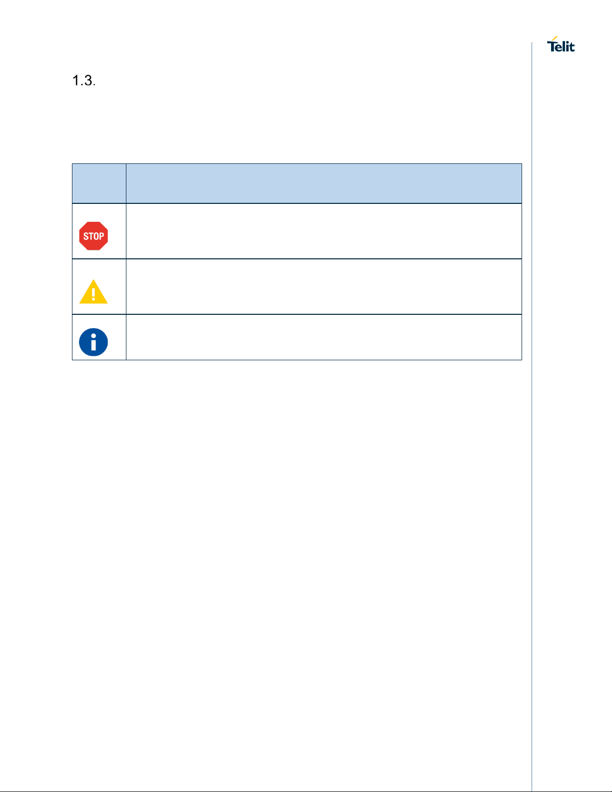
Caution or W arning – This is an important point about integrating the product
Tip – This is advice or suggestion that may be useful when integrating the
Text Conventions
• Dates are in ISO 8601 format, i.e. YYYY-MM-DD.
Symbol Description
Danger – This information MUST be followed or catastrophic equipment failure
and/or bodily injury may occur.
into a system. If this information is disregarded, the product or system may
malfunction or fail.
product.
1VV0301333 Rev. 2 Page 12 of 68 2017-06-27
Page 13

SL876Q5-A Product User Guide
Related Docum e nts
• SL876Q5-A Data Sheet
• SL876Q5-A Evaluation Kit User Guide
Related Documents Requiring a Non-disclosure Agreement
• SiRFstarV B02 Designer’s Guide
• SiRFstarV B02 Software User's Guide
• NMEA Reference Guide (CS-129435-MA8)
• SiRFstarV One Socket Protocol Interface Control Document (CS-129291-DCP15)
• SiRFstarV OSP Extensions (CS-303979-7)
1VV0301333 Rev. 2 Page 13 of 68 2017-06-27
Page 14

SL876Q5-A Product User Guide
2. PRODUCT DESCRIPTION
The SL876Q5-A modules are complete multi-constellation position, velocity, and time (PVT)
engines featuring high performance, high sensitivity, and low power consumption.
A built-in tri-band chip antenna receives RF signals from the GNSS satellite s. Provision is also
made for switching to an external active antenna under host control.
The inclusion of the GLONASS and BeiDou constellations yields better coverage, greater
accuracy, and improved availability.
The SL876Q5-A modules are based on the SiRFstar 5e (B02) flash GNSS chip.
Product Over view
• Complete GNSS receiver module including memory, LNA, TCXO, RTC, and tri-band
chip antenna
• External antenna may be used
• Based on the SiRFstar 5e (B02) flash GNSS chip
• GPS (L1), QZSS, and either Glonass (L1) or BeiDou (B1) simultaneous ranging
• Galileo ready
• SBAS capable (WAAS, EGNOS, MSAS, GAGAN), including ranging
• AGPS support for extended ephemeris using local or server-based solutions:
o Client-Generated Extended Ephemeris (CGEE)
o Server-Generated Extended Ephemeris (SGEE)
• Jamming Rejection
• Supports an external active antenna
• 1PPS output
• Fix reporting at 1 H z 5 Hz, or 10 Hz
• NMEA v3.1 command input and data output
• OSP (binary) command input and data output
• Two serial ports for input commands and output messages
• The primary serial port is configurable for UART, I
• The secondary serial port is configurable for UART or I
• 16 Megabit built-in flash memory
• Less than 70 mW typical power consumption (Full Power mode – GPS + GLO)
• Power management modes for extended battery life
o SiRFSmartGNSS I, SiRFSmartGNSS II
o Push-to-Fix, Trickle Power, SiRFaware
• Supported by evaluation kits
• -40°C to +85°C industrial temperature range
• 11.0 x 11.9 x 2.15 mm (nominal) 24-pad LCC package
• Surface mountable by standard SMT equipment
• RoHS compliant design
2
C, or SPI interface
2
Cinterface
1VV0301333 Rev. 2 Page 14 of 68 2017-06-27
Page 15
SL876Q5-A Product User Guide
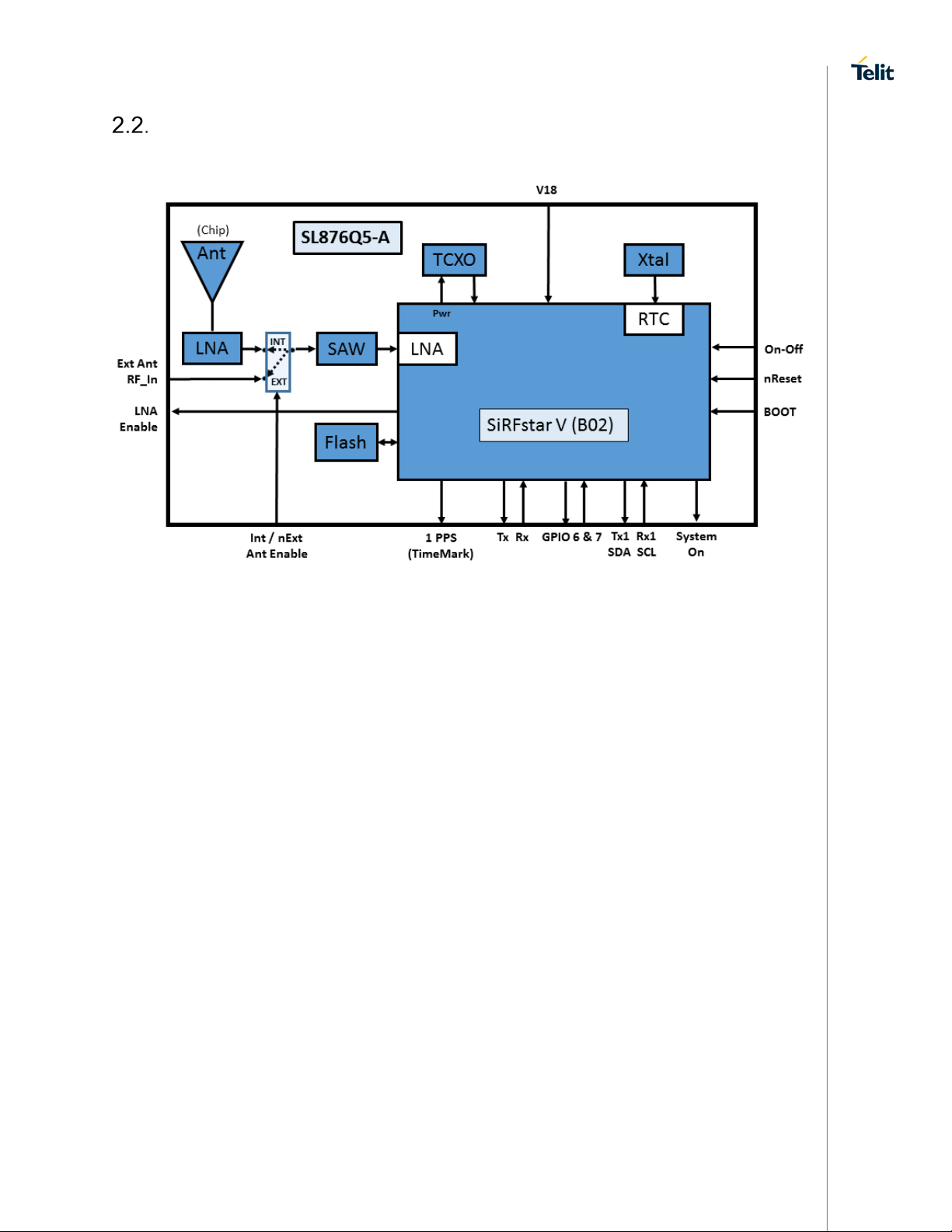
SL876Q5-A Block Diagram
Figure 2-1 SL876Q5-A Block Diagram
1VV0301333 Rev. 2 Page 15 of 68 2017-06-27
Page 16
SL876Q5-A Product User Guide
SL876Q5-A Module
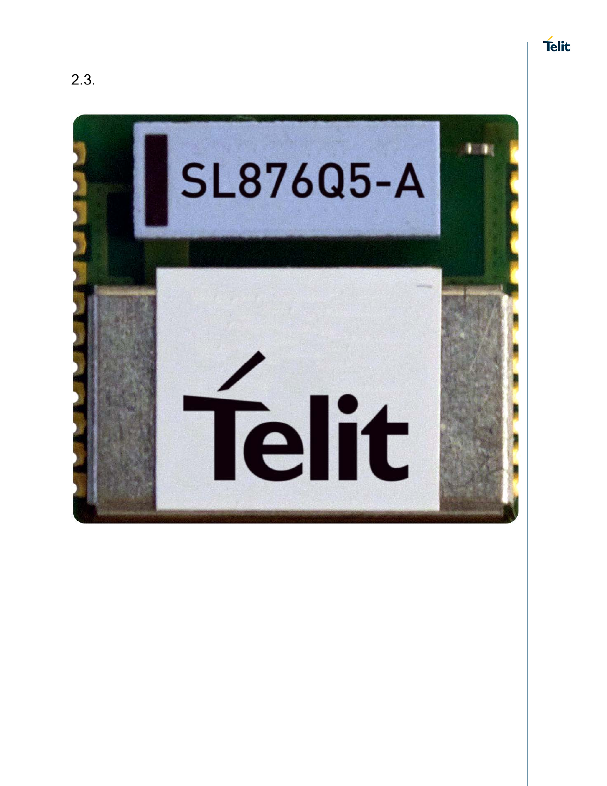
Figure 2-2 SL876Q5-A module photo
1VV0301333 Rev. 2 Page 16 of 68 2017-06-27
Page 17
SL876Q5-A Product User Guide
3. SL876Q5-A EVALUATION KI T (E V K)
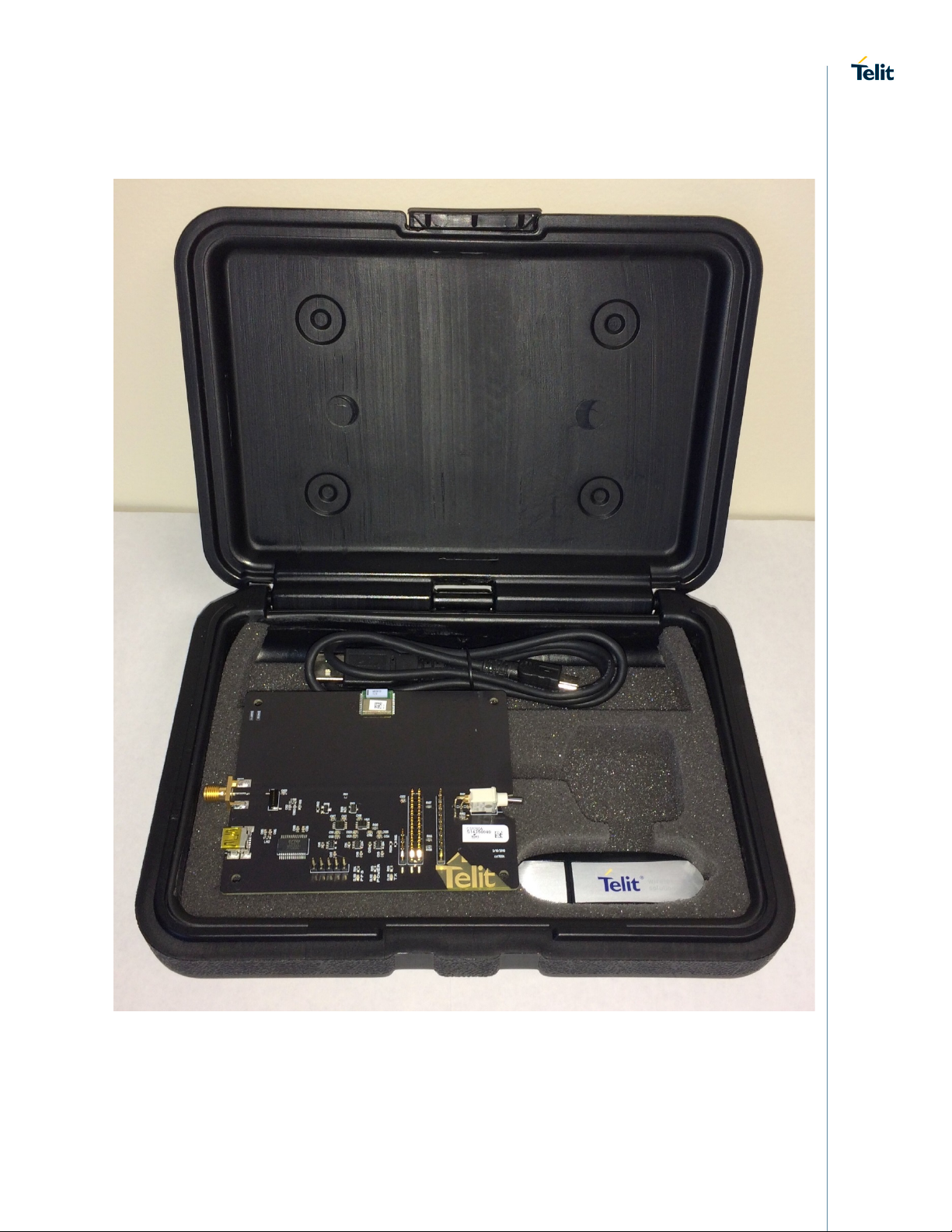
Figure 3-1 Evaluation Kit (EVK) contents
1VV0301333 Rev. 2 Page 17 of 68 2017-06-27
Page 18
SL876Q5-A Product User Guide
SL876Q5-A Evaluation Board (EVB)
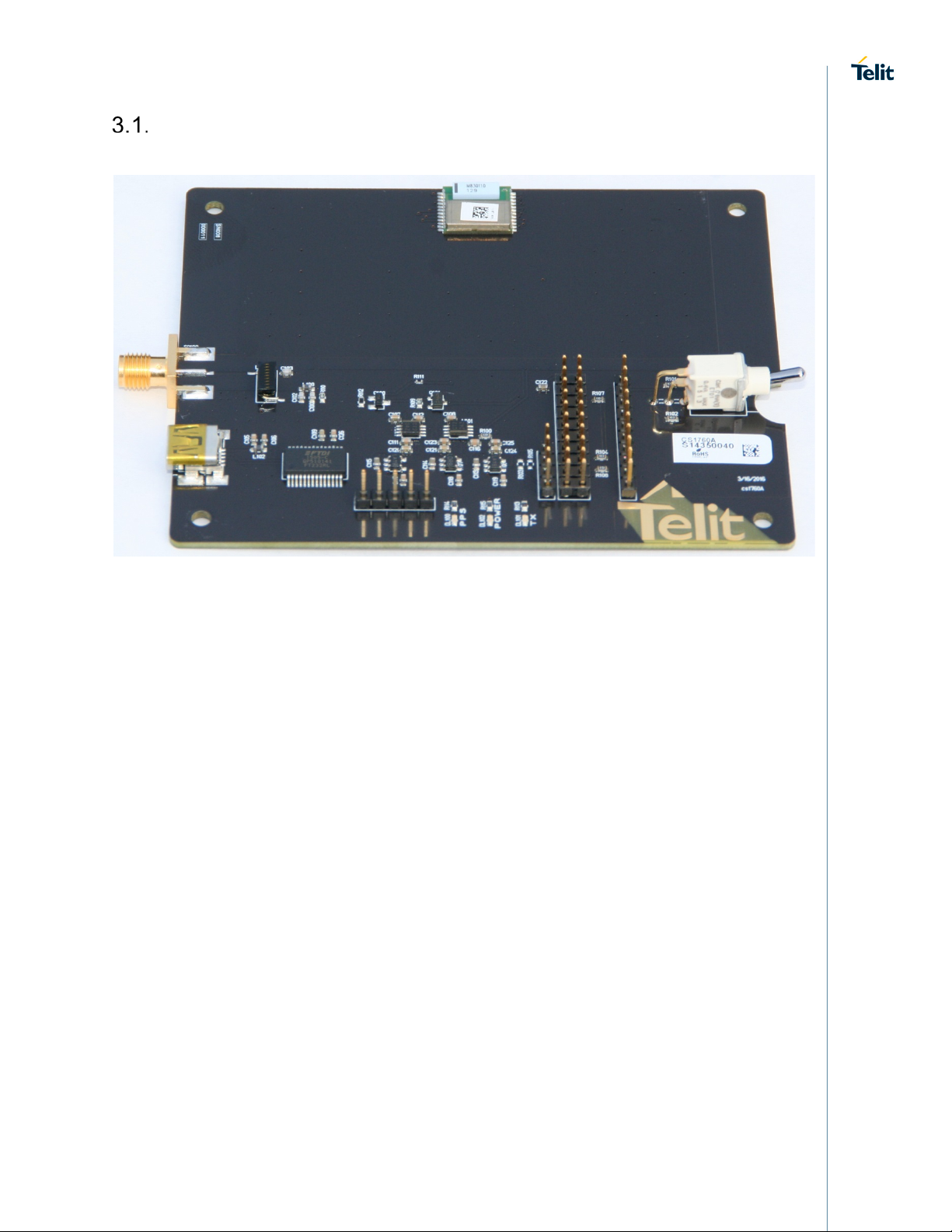
Figure 3-2 SL876Q5-A Evaluation Board
1VV0301333 Rev. 2 Page 18 of 68 2017-06-27
Page 19

SL876Q5-A Product User Guide
4. PRODUCT FEATURES
Built-in Antenna and Switch
The module includes a built-in tri-band chip ant enna and an RF switch that provides for input
from an external active antenna.
Multi-Constellation Navigation
GPS and GLONASS constellations are enabled by default.
The user may enable or disable GPS, GLONASS, and/or BDS constellations via OSP
command MID 222,16. Use of GLONASS or BDS alone may not give optimum positioning
results depending on the region that the receiver is located in.
Quasi-Zenith Satellite System (QZSS) support
The Japanese SBAS satellites are in a highly-inclined elliptical orbit which is geosynchronous
(not geostationary) and has analemma-like ground tracks. This orbit allows continuous
coverage over Japan using only three satellites. Their primary purpose is to provide
augmentation to the GPS system, but the signals may also be used for ranging.
QZSS ranging is disabled by default, but can be enabled via OSP MID 222,16 command.
Satellite Based Augmentation System (SBAS)
The receiver is capable of using SBAS satellites both as a source of differential corrections
and satellite ranging measurements. These systems (WAAS, EGNOS, GAGAN and MSAS)
use geostationary satellites to transmit regional corrections via a GNSS-compatible signal.
SBAS Corrections
The SBAS satellites transmit a set of differential corrections to their respective regions. The
use of SBAS corrections can improve positioning accuracy.
SBAS corrections for GPS are disabled by default but can be enabled via OSP MIDs 133, 138,
and 170 c ommands. Thereafter, the receiver will demodulate and use corrections data from
the SBAS signal.
SBAS Ranging
The use of SBAS satellites can augment the number of measurements available for the
navigation solution, thus improving availability and accuracy.
SBAS satellite ranging is disabled by default but can be enabled via a $PSRF103 MNEA
command or OSP Mode Control command (MID 136).
Assisted GPS (AGPS) - SiRFInstantFix™
A GNSS receiver requires ephemeris data to calculate the precise position in space of each
satellite to be used in the navigation solution. Since the satellites move at a speed of 3874
km/s along their orbits and are subject to gravitational perturbations from all masses in the
solar system, this data must be both current and accurate. Each GPS satellite transmits a
complete set of its ephemeris coefficients (called the broadcast ephemeris or BE) every 30
seconds. This is therefore the minimum time required for a cold start Time to First Fix (TTFF).
The BE data is usually refreshed every 2 hours.
1VV0301333 Rev. 2 Page 19 of 68 2017-06-27
Page 20

SL876Q5-A Product User Guide
The minimum cold start TTFF can be reduced from 30 seconds to just a few seconds by
implementing AGPS, which can provide Extended Ephemeris (EE) data by two methods -
1. Locally-generated: The receiver includes software to project the future positions of
the satellites. This data may be calculated out to 14 days or even longer, depending
on the resources available in the receiver, e.g. computation ability and memory.
2. Server-generated: A server calculates the future position projections and makes them
available to a receiver, typically over the internet. This data may be good for 30 days,
depending on available resources, e.g. communication links and storage.
Both CGEE and SGEE are available for GPS and GLONASS satellites.
Client-generated Extended Ephemeris (CGEE)
Extended ephemeris is computed in the receiver and then stored locally in the flash memory.
Whenever the module receives ephemeris data for a satellite, it checks if it has computed
CGEE for that satellite recently. If it has not, it computes EE for that satellite (for the next 3
days for GPS and 1 day for GLONASS) and stores it in flash memory. The next time the module
turns on and broadcast ephemeris is not available for a visible satellite, the stored CGEE data
is searched to see if it is still valid and can be used. If EE data is available for enough satelli tes,
the receiver can obtain a first fix in 10 to 15 secon ds (typical) rather than the usual 35 second s
without EE data. CGEE is enabled by default.
Server-generated Extended Ephemeris (SGEE)
Extended ephemeris is computed at the server and saved in a file which can then be
downloaded to the receiver’s flash memory. The server file contains 1, 3, 7, and 14, days of
ephemerides. To use SGEE data, a file must be transferred using NMEA or OSP commands.
Please contact Telit support for subscription details.
2-D Positioning
By default, the module will compute a 2-D solution if possible when performing initial
acquisition. In a 2-D solution, the receiver assumes a value for altitude and uses it to estimate
the horizontal position. Under warm and hot start conditions, the receiver uses the last known
value of altitude, which is a good assumption in most situations. However under cold start
conditions, the last position is unknown, and the receiver assumes a value of 0. In situations
where the true altitude is significantly higher than that, the horizontal position estimate will be
noticeably impacted. 2_D positioning is controlled by OSP MID 136.
Static Navigation
Static Navigation is an operating mode in which the receiver will freeze the position fix when
the speed falls below a set threshold (indicating that the receiver is stationary). The course is
also frozen, and the speed is reported as 0. The navigation solution is unfrozen when the
speed increases above a threshold or when the computed position exceeds a set distance
from the frozen position (indicating that the receiver is again in motion). These thresholds
cannot be changed by the user.
This feature is useful for applications in which very low dynamics are not expected, the classic
example being an automotive application.
Static Navigation is disabled by default, but can be enabled by OSP MID 143 command.
1VV0301333 Rev. 2 Page 20 of 68 2017-06-27
Page 21

SL876Q5-A Product User Guide
Velocity Dead-Reckoning
Velocity dead-reckoning is the use of the last known velocity to propagate the navigation
solution when there are insufficient measurements to calculate an updated solution. It serves
to mitigate the effects of blocked satellite signals by continuing to provide a position output.
Note: The receiver outputs status information which indicates that a solution is being
maintained using dead-reckoning.
This feature is disabled by default but can be enabled using the Mode Control message (MID
136). Valid timeout values are in a range from zero (which disables dead-reckoning) to two
minutes.
Jamming Rejection – Continuous Wave (CW) Jamming
Mitigation
Continuous Wave (CW) jamming mitigation improves performance in a system that is affected
by these predictable jamming signals:
• Stable jamming signals generated by your system implementation, such as
harmonics of digital clocks and logic switching
• Predictable jamming signals in the RF environment (e.g. from collocated transmitters)
When this feature is activated, the process for jamming mitigation is:
1. Detect jamming signals above the noise floor.
2. Isolate and filter frequencies containing jamming signals.
The GNSS signal is constantly monitored for CW jammers and up to eight are detected and
cancelled in each band without any operator intervention.
GPS, GLONASS, and BDS band cancellers are activated and reported using OSP Message
ID 92. This feature is useful both in the design stage and during the production stage for
uncovering issues related to unexpected jamming. Use OSP MID 220,1 to configure this
feature.
Elevation Mask Angle
The default elevation mask angle is 5° which can be changed using OSP MID 139.
5 Hz Navigation
When this feature is enabled, the receiver starts in 1 Hz mode and continues until it achieves
an over-determined fix with 5 or more satellites. It then computes and outputs solutions 5 times
per second. Each computation uses fewer, but more frequent satellite observations. In most
situations this gives a better response to vehicle velocity and course changes but might cause
slightly more erratic performance in stationary or low-dynamic situations.
The receiver also attempts to send out 5 times as many messages per second. The data rate
may need to be increased or the set of scheduled messages be reduced to avoid overloading
the available bandwidth.
For NMEA protocol, with default messages set on (GGA, GSA and RM C output once per cycle
and GSV output once every 5 cycles) output is nearly 1300 characters per second. Including
start and stop bits, at least 19200 bps is required to avoid running out of bandwidth.
For multi-constellation output, one GNGNS and one GNGSA would be added to each report
cycle, and three GNGSV sentences every 5
rate. For OSP protocol, CSR recommends a minimum data rate of 115200 bps.
1VV0301333 Rev. 2 Page 21 of 68 2017-06-27
th
cycle, r equiring a minimum of 38,400 bps data
Page 22

SL876Q5-A Product User Guide
To enable 5 Hz Navigation, use a $PSRF103 command or an OSP MID 136 command with bit
2 of the pos_mode_enable field set to 1.
10 Hz Navigation
When 10 Hz reporting is commanded, the output report rate is 10 Hz.
1PPS
The module provides a 1PPS timing pulse output. See Section 8.6.1 1PPS for d etails.
I/O Communication Ports
The 1st host port c an be configured to communicate us ing UART, I2C, or SPI interf ace and supports
UART Device Wakeup.
The 2nd host port can be configured for UART or I
See section 8.8 Host I/O Ports - Configuration and Operation for details.
2
C interface and supports I2C MEMS wakeup.
1VV0301333 Rev. 2 Page 22 of 68 2017-06-27
Page 23

SL876Q5-A Product User Guide
Power Management
The receiver features several operating modes that provide reduced power consumption.
Availability of GNSS signals in the operational environment will be a factor in choosing power
management modes. The designer can choose a mode that provides the best trade-off of
navigation performance versus power consumption.
Each of the power management modes can be commanded using the Power Mode Request
Message (MID218,6). Please refer to the SiRFstarV OSP Extensions manual (CS-303979) for
details.
Power Mode Name Description
Full Power
Continuous operation in reporting position
Continuous
SiRFSmartGNSS 1
Fixes
SiRFSmartGNSS 2
fixes optimized for the best all-around
performance.
SmartGNSS modes save power based on
satellite signal strength.
Trickle Power Power cycling: RUN - STANDBY
Periodic Fixes
No Fixes Hibernate Only RTC and BBRAM are powered up.
Push To Fix Power cycling: RUN - HIBERNATE
SiRFAware Periodic data collection & updating
Table 4-1 Power Management Modes
Full Power Mode
This mode has the highest average power consumption, but it is the most accurate navigation
mode and supports the most dynamic motion scenarios. Full Power is required during initial
satellite acquisition, tracking, & navigation and while receiving SGEE assistance data.
SmartGNSS
SmartGNSS modes are power saving alternatives for GNSS operation while maintaining
complete functionality of the device similar to full power mode.
1VV0301333 Rev. 2 Page 23 of 68 2017-06-27
Page 24

SL876Q5-A Product User Guide
The module defaults to full power during the initial acquisition of the first fix, and will continue
tracking in SmartGNSS if enabled. Therefore, all first fix metrics for SmartGNSS are equivalent
to full power.
4.15.2.1. SmartGNSS I SmartGNSS I autonomously manage GNSS system usage based on signal conditions to save
power. This is the default.
The adaptive mechanism uses fewer system resources during strong signal conditions and
uses more resources during weak signal conditions in order to maintain navigation
performance. Full constellation tracking is maintained while in this mode. 1PPS is available.
4.15.2.2. SmartGNSS II SmartGNSS II includes the benefits of SmartGNSS I and achieves further power reduction by
minimizing the usage of the secondary GNSS constellation. The adaptive mechanism adjusts
constellation usage based on signal conditions to maintain performance while minimizing
power consumption. 1PPS is available.
Trickle Power
This mode cycles between FULL POWER and STANDBY states. It provides GPS-only
navigation updates at a fixed rate of 1 to 10 seconds, and retains good acc uracy and dynamic
motion response, but at a lower average power consumption than Full Power. The receiver will
go to FULL POWER if signals are weak or the fix is lost. 1PPS is not available. TricklePower
mode yields significant power savings in strong signal conditions.
Push-to-Fix
This mode provides for even lower power consumption than TricklePower and is intended for
applications that require relatively infrequent position reports. The position is reported
periodically (once every 6, 12, 18, 24 seconds or 30 to 86400 seconds in 30 s increments) and
also when requested by toggling the On-Off pin.
Push-to-FixII allows vehicle velocity to be taken into account for PTF period, and QoS checks
to be enabled or disabled.
SiRFaware
This is a power-saving mode that maintains GPS data by waking up at intervals (e.g. every 30
minutes) to collect signals. Time/and position estimates are updated (e.g. every 10 minutes).
Extended Ephemeris will be used if available.
Hibernate
The receiver can be commanded into the HIBERNATE state, which is the lowest power mode
available. Only the RTC and BBRAM domains are pow ered up. Use the NMEA $PSRF117,16
or OSP MID 205 command to transition to this state. The module will also transition to
HIBERNATE when the ON-OFF pin is brought low.
1VV0301333 Rev. 2 Page 24 of 68 2017-06-27
Page 25

SL876Q5-A Product User Guide
Internal LNA
The module has an adjustable gain LNA internal to the GNSS device.
An additional LNA is in the module circuit for the built-in chip antenna. It is not in the circuit for
an external antenna.
Internal antenna LNA power is controlled by the LNA Enable output line. This line may also
be used to control the external antenna LNA power (when Internal / nExternal_Ant_Enable
is active).
Device Wake-up (1st port)
The module will wake up from a commanded HIBERNATE state if the ON_OFF signal remains
high and there is data traffic on serial port 0 (first port). The wake-up message will not be acted
upon since the receiver is not operating until after wake-up.
See section 8.8.1 Primary Host Port Configuration for configurationdetails.
MEMS Wakeup (2nd Port - I2C)
If the 2nd port is operating as I2C, the module can configur e a Kionix KXCJ9 MEMS acc elerometer to
generate a signal when a threshold is ex ceeded. This signal can be connecte d to a GPIO external
interrupt which will cause the module to wake up from a low power state. Use of this feature will require
a custom configured firmware build. See section 8.8.2 Secondary Host Por t Configuration for details.
Please contact Telit support for further details.
Host I/O Ports
The primary host port (TX / RX) can be configured to communicate using UART, I2C, or SPI
interface.
2
The secondary hos t port (TX1 / RX 1) can be configured to communicate using UART or I
interface.
See Section 8.8 Host I/O Ports - Configuration and Operation for det ails.
C
1VV0301333 Rev. 2 Page 25 of 68 2017-06-27
Page 26

SL876Q5-A Product User Guide
GPS
≤ 1.5
GPS + BeiDou
≤ 2.5
Hot
≤ 1.1
Warm - Assisted
7.5
Warm
22.3
Cold
31
Hot
≤ 1.1
Cold
27
Hot
≤ 1.1
Warm
29.7
Cold
32.2
5. PRODUCT PERFORMANCE
Horizontal Position Accuracy
Constellation CEP (m)
BeiDou N/A
GPS + Glonass ≤ 1.5
Test Conditions: 24-hr Static, -130 dBm, Full Power mode
Table 5-1 SL876Q5-A Horizontal Position Accuracy
Time to First Fix
Constellations(s) Start Type Max TTFF (s)
GPS
GPS + GLO
GPS + BeiDou
Warm 22.8
1VV0301333 Rev. 2 Page 26 of 68 2017-06-27
Test Conditions: Static scenario, -130 dBm, Full Power mode
Table 5-2 SL876Q5-A Time to First Fix
Page 27

SL876Q5-A Product User Guide
Acquisition
-148
Navigation
-161
Tracking
-165
Acquisition
-148
Navigation
-161
Tracking
-165
Sensitivity
Constellation(s) State
GPS
GPS + GLO
Test conditions: Static scenario, Full Power mode
Table 5-3 SL876Q5-A Sensitivity
Minimum Signal Level
(dBm) External Ant
1VV0301333 Rev. 2 Page 27 of 68 2017-06-27
Page 28

SL876Q5-A Product User Guide
1
GNSS Dilution of Precision (DOP) and active
1
• NMEA-0183 V3. 10
6. SOFTWARE INTERFACE
The host serial I/O port (UART, I2C, or SPI) supports full duplex communication between the
receiver and the user.
The default UART configuration is: NMEA, 9600 bps, 8 data bits, no parity, 1 stop bit.
Two protocols are available for command input and data output:
• SiRF One Socket Protocol (OSP)
NMEA Output Messa ge s
Defaults:
• NMEA-0183
• 1 Hz fix rate. Maximum is 10 Hz.
Standard Messages
These messages are sent by default.
Message ID Description
RMC GNSS Recommended minimum navigation data
GGA GNSS position fix data
GSA
satellites
GSV GNSS satellites in view.
Note: Multiple GSA and GSV messages may be output per cycle.
Table 6-1 Default NMEA Output Messages
The following messages can be enabled by command:
Message ID Description
GLL Geographic Position – Latitude & Longitude
VTG Course Over Ground & Ground Speed
Frequency
1
1 / 5
ZDA Time and Date
GNS GNSS Fix Data
Table 6-2 Available NMEA Output Messages
1VV0301333 Rev. 2 Page 28 of 68 2017-06-27
Page 29

SL876Q5-A Product User Guide
Talker ID
Constellation
The following Talker IDs are used:
GA Galileo
GB BeiDou
GL GLONASS
GP GPS
GN Solutions using multiple constellations
Table 6-3 NMEA Talker IDs
SiRF Proprietary Messages
The receiver can issue several proprietary NMEA output messages ($PSRF) which report
additional receiver data and status information.
Some of these messages exceed the 80-character limitation of the NMEA-0183 standard.
Telit Proprietary Messages
6.1.3.1. RF Input Status (Internal vs. External) To query the status of the RF input, send the command: $PTWS,ANT,INPUT,GET*77 A message indicating the RF input source (Internal vs. External Antenna) will be output.
$PTWS,ANT,INPUT,VAL,INTERNAL,1*AC (default)
or
$PTWS,ANT,INPUT,VAL,EXTERNAL,0*57
1VV0301333 Rev. 2 Page 29 of 68 2017-06-27
Page 30

SL876Q5-A Product User Guide
NMEA Input Commands
The receiver uses NMEA proprietary messages for commands and command responses. This
interface provides configuration and control over selected firmware features and operational
properties of the module.
The format of a command is:
$<command-ID>[,<parameters>]*<cr><lf>
Commands are NMEA proprietary format and begin with “$PSRF”.
Parameters, if present, are comma-delimited as specified in the NMEA protocol.
Change output sentences and their rates
Use the Query/Rate Control ($PSRF103) command to enable and disable output NMEA
messages and set their output rates.
Change data rate
Use the Set Serial Port ($PSRF100) command to change the port data rate.
Switch to OSP protocol
Use the Set Serial Port ($PSRF100) command to switch to the OSP protocol. It may be
necessary to change the data rate since OSP can generate a much larger volume of output
per reporting cycle.
OSP Output Messages
Please refer to SiRF OSP documentation.
OSP Input Commands
Change output messages
Use OSP MID 166 to change the output messages.
Change data rate
Use OSP MID 134 to change the baud rate
Switch to NMEA protocol and da ta rate
Use the OSP MID 129 command to switch to the NMEA protocol and change the port data
rate.
1VV0301333 Rev. 2 Page 30 of 68 2017-06-27
Page 31

SL876Q5-A Product User Guide
7. FLASH UPGRADABILITY
The firmware stored in the internal Flash memory of the SL876Q5-A may be upgraded via the
serial port TX/RX pads.
Please refer to the SL876Q5-A Evaluation Kit User Guide to update the firmware.
1VV0301333 Rev. 2 Page 31 of 68 2017-06-27
Page 32

SL876Q5-A Product User Guide
8. ELECTRICAL INTERF ACE
Module Pin-out
Figure 8-1 SL876Q5-A Pin-out Diagram
1VV0301333 Rev. 2 Page 32 of 68 2017-06-27
Page 33

SL876Q5-A Product User Guide
ON
be
SEL may be pulled high to
SEL is read
prior to the host select lines (GPIO 6 & 7). This pin should be
GPIOs 6 & 7 a re read during power-u p and res et to conf igur e the
After configuration, they may be used for UART or SPI signal lines
See Section 8.8 Host I/O Ports - Configuration and Operation.
Enable
Enable the internal Chip Antenna
See Section 8.5.4 Internal / nExternal Antenna Enable
power state.
Pin Name Type Function
Power
18 1V8 Pwr
Connect to 1.8 V supply. See Section 8.4 Power Supply.
Ground
2, 3, 5,
10,
12,
13,
20, 24 GND Gnd Connect all pins to ground.
RF Input
11
Ext Ant
RF_In I
External Antenna RF Input. Max 16V DC may be applied.
See Section 8.7 RF Interface.
Control Input
On/Off. See Section 8.5.1
7 ON-OFF I
(output).
Reset (active low). Do not drive high. See Section 8.5.2 nReset.
This signal is not necessary for normal operation and should
1 nRESET I
brought out to a test point or may be left unconnected.
Low during normal operation. BOOT-
force the module into the programmable state. BOOT-
ON-OFF (input) and SYSTEM-
BOOT-
4
Select I
16 GPIO6
6 GPIO7
brought out to a test point or left floating.
See Section 7 Flash Upgradability.
primary host port.
depending on the firmware options enabled.
I
Int / nExt
14
Ant
(and disable the external (active) antenna). Internal pullup.
I
Output
Indicates the power state of the module. Also called Wakeup.
See Section 8.5.1 ON-OFF (input) and SYSTEM-ON (output).
22
System
On O
LNA control (used for both internal and external antennas).
LNA
9
Enable O
8 PPS O
High when the receiver is operating, low w hen in a lowAlso called GNSS_ON. See Section 4.16 Internal LNA.
1PPS time mark. See Section 8.6.1 1PPS.
1VV0301333 Rev. 2 Page 33 of 68 2017-06-27
Page 34

SL876Q5-A Product User Guide
Primary Host Communications Port I/O.
See Section 8.8 Host I/O Ports - Configuration and Operation
Primary Host Port Output.
17 TX O
UART: TX, I2C: CLK, or SPI: Data Out (MISO).
Primary Host Port Input.
15 RX I
UART: RX, I2C: DIO, or SPI: Data In (MOSI).
16 GPIO6 I/O After configuration, may be used for UART: nCTS or SPI: CLK.
6 GPIO7 I/O After configuration, may be used for UART: nRTS or SPI: nCS.
23 GPIOA
I2C Data Ready Indicator
Secondary Host Communications Port I/O
See Section 8.8 Host I/O Ports - Configuration and Operation
19
21
SCL /
RX1 I/O
SDA /
TX1 I/O
Secondary Host Port I/O.
UART: Receive (RX1), or I2C: Clock (SCL)
Secondary Host Port I/O.
UART: Transmit(TX1), or I2C: Data (SDA)
Table 8-1 SL876Q5-A Pin-out Function Table
1VV0301333 Rev. 2 Page 34 of 68 2017-06-27
Page 35

SL876Q5-A Product User Guide
Tristate output leakage at VO = 1.8 V
or 0 V
CI
Input capacitance, digital output
- 8 -
pF
ESD Voltage CDM
JESD22-C101E
ESD Voltage HDM
JEDEC JS-001-2012
DC Characteristics
Signal Description Min Typ Max Units
VOL Low level output voltage, IOL 2mA 0.0 - 0.22 x VDD V
VOH High level output voltage, IOH 2mA 0.8 * VDD - VDD V
VIL Low level input voltage -0.3 - 0.3 x VDD V
VIH High level input voltage, IIH 2mA 0.7 x VDD - VDD + 0.3 V
RPU Internal pull-up resistor equivalent 50 86 157 kΩ
RPD Internal pull-down resistor equivalent 51 91 180 kΩ
LI Input leakage at VI = 1.8 V or 0 V -10 - 10 µA
LO
-10 - 10 µA
Table 8-2 DC Characteristics
Absolute Maximum Ratings
Parameter Pins Absolute Max Rating Units
RF Input Voltage All RF inpu t s 1.5 V
RF Input Power All RF inputs 10 dBm
All Pins
All Pins
± 1100
± 500
1.8 V Supply Voltage 1V8 2.2 V
V
V
I/O Pin Voltage All digital inputs 3.60 V
1VV0301333 Rev. 2 Page 35 of 68 2017-06-27
Table 8-3 Absolute Maximum Ratings
Page 36

SL876Q5-A Product User Guide
1V8
1.71
1.8
1.89
V
Max ripple: 54 mV (0 to 3 MHz), 15 mV (> 3 MHz)
Power Supply
1.8 V Supply Voltage
Unlike previous GNSS receiver modules, the SL876Q5-A requires a single always-on 1.8 V
supply. Rather than having a “split” power supply design of main and backup, the module
manages all of its power modes internally. The module will power up into the state determined
by the ON-OFF pin (High: RUN; Low: HIBERNATE).
The current power state of the SL876Q5-A can be determined by monitoring the “SYSTEMON” signal. A logic low indicates the module is in OFF, RESET, HIBERNATE, or STANDBY;
whereas logic high indicates the module is in RUN state.
If the 1.8 volt DC supply is removed from the module (regardless of power state) it will lose
current RTC time and the contents of the internal SRAM. To execute an orderly shutdown,
place the module into the HIBERNATE state, then remove power. To prevent improper startup,
keep the power removed for approximately 10 seconds to reliably clear the SRAM contents.
The module monitors the 1.8 volt supply and issues an internal hardware reset if the supply
drops below 1.7 volts. This reset protects the memory from accidental writes during a power
down condition. This reset forces the module into a low power stand-by state.
To prevent the reset, the 1.8 volt supply must be regulated to be within ±50 mV of nominal
voltage (including load regulation and power supply noise and ripple). Noise and ripple ou tside
of these limits can affect GNSS sensitivity and also risk tripping the internal voltage
supervisors, thereby shutting down the module unexpectedly. Regulators with very good load
regulation are strongly recommended along with adequate power supply filtering to prevent
power supply glitches as the module transitions between power states.
The power supply voltage, including noise and ripple must be as specified below in Table 8-4
DC Supply Voltage for all frequencies. To help meet these re quirements, a sepa rate LDO for
the module is suggested.
Voltage Supply Capacitance
Aluminum electrolytic capacitors are not recommended at the input to the module due to their
high ESR. Tantalum capacitors are recommended with a minimum value of 10uF in parallel
with a 0.1uF ceramic capacitor. Ceramic capacitors alone can be used, but ensure that the
LDO is stable with such capacitors tied to the output.
DC Power Requirements
Name Min Typ Max Units
Table 8-4 DC Supply Voltage
1VV0301333 Rev. 2 Page 36 of 68 2017-06-27
Page 37

SL876Q5-A Product User Guide
Low Power Modes
Low Power Mode
Typ
Units
Trickle Power mode: On 100 ms, Max Off 30 s
DC Power Consumption
Power Mode -> Ful l Power
State & Constellation Typ Max Units
Acquisition
GPS only 65 77 mW
GPS and Glonass 84 89 mW
Navigation/Tracking
GPS Only 53 67 mW
GPS and Glonass 70 80 mW
Table 8-5 Power Consumption – SL876Q5-A
Trickle Power 15 mW
Push to Fix 17 mW
Battery Backup (Hibernate) 68 uW
Push To Fix mode: Interval: 6 s, Max Search: 6 s, Max Off: 120 s
Table 8-6 Power Consumption – SL876Q5-A Low Power modes
1VV0301333 Rev. 2 Page 37 of 68 2017-06-27
Page 38

SL876Q5-A Product User Guide
Control Input Signals
ON-OFF (input) and SYSTEM-ON (output)
The SL876Q5-A module has three power states: OFF, RESET, and ON.
The OFF state is when power is removed from the module.
Upon initial application of power, the module enters the RESET state until the internal reset
process is completed. It then transitions to the ON state.
In the ON state, the module will transition to either the RUN or HIBERNATE substate
depending on the ON-OFF pin status.
If the ON-OFF pin is high, the module will transition to the RUN substate.
If the ON-OFF pin is low, the module will transition to the HIBERNATE substate.
The ON state is indicated by a logic high output on the SYSTEM-ON signal.
Note: The ON_OFF pin must not be tied to V18 because it must be brought low, then high to
transition out of a commanded hibernate state.
The module will transition to the RESET state when external reset (nRESET) is pulled low, or
upon internal reset (e.g. supply voltage out of spec). The external nRESET signal takes
precedence over the state of the ON-OFF signal. SYSTEM-ON will be logic low.
While in the ON state, there are three substates, depending upon commands or selected power
management modes. The three substates are: HIBERNATE, STANDBY, and RUN.
The module transitions between RUN and STANDBY via TricklePower modes; and between
RUN and HIBERNATE via PushToFixII and SiRFaware modes. It can also transition from RUN
to HIBERNATE by de-asserting the O N-OFF signal. The firmware is configured to transition
from HIBERNATE to RUN when data is received on the RX pin.
In HIBERNATE and STANDBY, the SYSTEM-ON signa l will be logic low; in RUN, it will be
logic high.
To execute an orderly shutdown, place the module in the HIBERNATE substate, then remove
power.
Also, see Section 8.5.2 nReset.
nReset
The module will generate an internal reset as appropriate. Therefore, no external signal is
required for the module to operate properly and this pin may be left unconnected. However, it
is desirable to bring it out to a test point if otherwise unconnected.
If an external reset is desired, the signal must be either open collector or open drain without
any form of pull up. Do not pull this line high with either a pull up or a driven logic one. When
this line is pulled low, the module will immediately transition into reset mode.
When the external reset is released, the module will go through its normal power up sequence
provided the V18 supply is within specifications. See Section 8.5.1 ON-OFF (input) and
SYSTEM-ON (output).
Pulling nRESET low at any time forces the module into the reset state irrespective of the ONOFF signal. In the reset state, the SYSTEM-ON signal is low.
Once the nRESET signal is released the module will transition to the HIBERNATE state or to
the ON state as determined by the ON-OFF signal input.
1VV0301333 Rev. 2 Page 38 of 68 2017-06-27
Page 39

SL876Q5-A Product User Guide
Boot Select
It is not necessary to use the Boot Select pin to re-flash the receiver since SiRFlive can use
commands to perform this tas k. However, it is desirable to bring it out to a test poin t if otherwise
unconnected.
Internal / nExternal Antenna Enable
When high, the module enables RF input f rom the internal chip antenna and disables input
from the external antenna.
When low, the external antenna is enabled and the LNA Enable signal may then be used to
control power to the external LNA according to the power state of the receiver (operating or
low-power).
This pin has an internal pullup which makes the internal antenna the default RF input.
See Section 8.6.3 LNA Enable.
Control Output Signals
1PPS
1PPS is a one pulse per second signal which is enabled after the receiver has achieved a 5satellite Kalman filter position fix. It is disabled when the position fix becomes invalid. However,
if Velocity Dead Reckoning is enabled, the pulse is continued until its timeout has expired.
The time mark is within 1 μs of the GPS epoch and normally within 100 ns.
Pulse width is 250 ms.
SYSTEM-ON (output)
See Section 8.5.1 ON-OFF (input) and SYSTEM-ON (output).
LNA Enable
This signal indicates the power state of the module. It is high when the receiver is operating
and can accept an RF input. When the receiver is in a low-power state, it does not accept RF
input, therefore the LNA can be turned off to save power.
This signal controls the internal chip antenna and may also be used to control the external
antenna LNA if desired.
1VV0301333 Rev. 2 Page 39 of 68 2017-06-27
Page 40

SL876Q5-A Product User Guide
Ground Plane Performance Reduction (approximate)
40 mm x 20 mm
-10
RF Interface
Built-in chip antenna
The SL876Q5-A module includes an internal chip antenna and LNA which is used when the
Internal / nExternal_Ant_Enable signal is high. See Section 8.5.4 Internal / nExternal
Antenna Enable. For important information regarding the required ground plane, see Section
8.7.3 Ground Plane
External RF Input
When the Internal / nExternal_Ant_Enable signal is low, the RF input (External Antenna
RF_In) pin accepts GNSS signals in the range of 1561 MHz to 1606 MHz at a level between
-125 dBm and -151 dBm into 50
Antenna Enable.
The LNA_Enable output signal may be used to control power to the External Antenna LNA
(when it is selected).
A maximum of 16 V DC can be applied to the RF input.
The RF-IN pin is ESD sensitive.
Ω impedance. See Section 8.5.4 Internal / nExternal
An active antenna (that is, an antenna with a built in low noise amplifier) with a noise figure of
less than 1.0 dB should be used for optimum results. The SL876Q5-A contains an internal preselect SAW filter which is in both the External and Internal antenna input paths.
The chipset is in the Low Gain confi guration by default This is the correct choice for the internal
chip antenna and an external active antenna. Using an exte rnal passiv e a ntenna (w hi ch is not
recommended) would require changing the gain to High via an OSP command.
Ground Plane
Due to the very small size of the built-in chip antenna, a proper ground plane is critical to
achieving good performance. Please refer to Figure 12-1 SL876Q5-A Footprint and Ground
Plane for ground plane requirements.
The recommended minimum size is 40 mm x 80 mm. Using a smaller size ground plane will
result in significant performance degradation. Please note that the guideline values in the table
below are only a very rough approximation since there are many variables that affect the
results.
Size Signal Strength (relative) dB
40 mm x 80 mm -0
40 mm x 60 mm -5
40 mm x 40 mm -7
Table 8-7 Ground Plane Size
1VV0301333 Rev. 2 Page 40 of 68 2017-06-27
Page 41

SL876Q5-A Product User Guide
Signal
Frequency (MHz)
TCXO Frequency
26.000
Signal
Level
External Active Antenna V ol tage
An external bias-T is required to provide voltage to an external antenna. A maximum of 16 V
DC may be applied to the External Ant. RF_In pin. See Section 10.11 Powering an External
LNA (External Active Antenna).
Burnout Protection
The receiver can accept an external RF signal of up to -20 dBm with a DC voltage of ± 15 V
without risk of damage.
Jamming Rejection
Jamming Rejection can be used for solving narrow band (CW) EMI problems in the customer’s
system. It is effective against narrow band clock harmonics. Jamming Rejection is not effective
against wide band noise, e.g. from a host CPU memory bus or switching power supply because
these sources typically cannot be distinguished from thermal noise. A wide band jamming
signal effectively increases the noise floor and reduces GNSS signal levels.
Please refer to Section 4.9 Jamming Rejection – Continuous Wave (CW) Jamming
Mitigation for further details.
Frequency Plan
LO Frequency 1588.6
Table 8-8 Frequency Plan
Local Oscillator Leakage
LO Leakage -70 dBm (typical)
Table 8-9 LO Leakage
1VV0301333 Rev. 2 Page 41 of 68 2017-06-27
Page 42

SL876Q5-A Product User Guide
Pin
Pullup /
UART
I2C
SPI
GPIO6
Pullup
Float
Float
Weak
Float
Pulldown
Float
Host I/O Ports - Configuration and Operation
The module host serial ports are configurable for the desired interface.
2
The primary host port can be configured to communicate using a UART, I
See Section 8.8.1 Primary Host Port Configuration for details of port configuration.
Also, see Section 4.17 Device Wake-up for this port.
Default port configuration is UART, NMEA at 9600 bps, 8-bit, No parity, and 1 stop bit.
The secondary host port can be configured to communicate using a UART or I2C interface.
SPI is not available because it requires 4 pins.
Primary Host Port Configuration
The module includes a full-duplex serial interface which is configured for UART, I2C or SPI
interface by reading GPIO6 and GPIO7 pins at startup or reset (only).
The following table gives the required input signals:
C, or SPI interface.
Pulldown
(multi-master)
(slave)
Weak
GPIO7
internal
pulldown
internal
pullup
10 kΩ to +1.8 V
(may become CTS)
(may become RTS)
10 kΩ to ground
(becomes SCLK)
(becomes SPI_CS)
Table 8-10 Primary Host I/O Port Configuration
Note: The GPIO6 and GPIO7 lines are read for configuration purposes at power up or reset
only. Afterwards, they may be used for UART or SPI signal lines depending on firmware
options.
Secondary Host Port Configuration
The secondary Port is configured by loading the desired FW build.
UART Operation
Upon power up, the module will communicate using a standard asynchronous 8 bit protocol
with output messages appearing on the TX line and input commands and data being received
on the RX line. The UART can operate at baud rates from 4800 bps to 1.2 288 Mbps, however
speeds above 115,200 bps have not been fully tested and verified.
If the module is operated in TricklePower mode, a baud rate of at least 38,400 is
recommended. This reduces the time required to empty the output buffer and allows the
receiver to drop into the low power state for a longer period of time.
The minimum recommended baud rate for OSP is 38400, or 115200 if debug data messages
are enabled.
1VV0301333 Rev. 2 Page 42 of 68 2017-06-27
Page 43

SL876Q5-A Product User Guide
TX
Transmit Data (TX)
Secondary Port
TX1
Trans mit Data (TX1)
RX1
Receive Data (RX1)
Use the Query/Rate Control (PSRF103) to enable and disable output NMEA messages and
set their output rates.
After configuration, the pins are defined below:
Pin Name UART Function
Primary Port
RX Receive Data (RX)
GPIO6 nCTS
GPIO7 nRTS
Table 8-11 UART Pin Assignments
Note: Flow control is disabled by default.
Use the OSP MID 178,70 command to enable/disable flow control on the first port.
I2C Operation
See Section 8.8.1 Primary Host Port Configuration to specify I2C interface. Upon power up,
the module acts as a master transmitter and a slave receiver (multi-master mode).
• When used in I2C mode, pull-ups in the range of 1K to 2.2K to a 1.8V to 3.6V power
supply are required on the RX and TX lines.
Clock rates of 100 and 400 kbps are supported.
2
The operation o f the I
where both the module and the host can independently freely transmit. It is possible to enable
the master transmit and slave receive at the same time, as the I
resolution between module and host vying for the bus.
C with a master transmit and slave receive resembles a UART operation,
2
C bus allows for contention
1VV0301333 Rev. 2 Page 43 of 68 2017-06-27
Page 44

SL876Q5-A Product User Guide
GPIO7
Not used
GPIOA
Data Ready
Secondary Port
Primary Port
TX
SPI Data Out (MISO)
Not Available
After configuration, the pins are defined below:
Pin Name I2C Function
Primary Port
TX I2C Clock (SCL)
RX I2C Data (SDA)
GPIO6 Not used
TX1
I2C Data (SDA)
RX1 I2C Clock (SCL)
Table 8-12 I
2
C Pin Assignments
SPI Operation
See Section 8.8.1 Primary Host Port Configuration to specify SPI interface.
nd
The 2
SPI is supported in the slave mode. The MicroWire format is not supported.
Maximum speed is 6.8 MHz.
After configuration, the pins are defined below:
port cannot be configured for SPI interface since there are only two pins available.
Pin Name SPI Function
RX SPI Data In (MOSI)
1VV0301333 Rev. 2 Page 44 of 68 2017-06-27
GPIO6 SPI Clock (SCLK)
GPIO7 SPI Chip Select (CS#)
Secondary Port
Table 8-13 SPI Mode Pin Assignments
Page 45

SL876Q5-A Product User Guide
9. REFERENCE DESIGN
Figure 9-1 Reference Design
1VV0301333 Rev. 2 Page 45 of 68 2017-06-27
Page 46

SL876Q5-A Product User Guide
Please refer to Section 8 Electrical Interface for important det ails for each pin.
Along with power and ground, the signals required to operate the module properly are: an
external antenna RF input (optional), a UART TX/RX pair, and several control lines as
described below.
The power supply must have tight voltage regulation under varying line and load conditions to
prevent falsely tripping the internal voltage supervisor within the module. See Section 8.4
Power Supply for details of requirements for the power supply.
Due to the very small size of the built-in chip antenna, a proper ground plane is critical to
achieving good performance. Please refer to Figure 12-1 SL876Q5-A Ground Plane for
requirements.
An optional ac tive GNSS antenna can be connected through C1 (which is used to block DC
voltage) to the External_Ant_RF_Input pin. The referenc e design shows a DC power feed for
the external antenna’s LNA which is controlled by the state of the module (operating vs. low
power) on the LNA_ENABLE pin. The inductor L1 is chosen to be self-resonant at the GPS L1
frequency (1.57542 GHz) to minimize loading on the RF trace. Capacitor C3 is also chosen to
be self-resonant to provide a near short at that RF frequency. The internal chip antenna is
enabled by grounding the INT/nEXT_Ant_En pin through JP3.
The TX/RX serial port can be configured for UART, I
2
C, or SPI interface using GPIO 6 and 7.
As shown, GPIO7 is floating and resistor R4 pulls GPIO6 high, which specifies the host port
confi gurat ion to be U ART. See Section 8.8 H ost I /O Por ts - Configuration and Operation
for details.
TX an d RX ar e a standard serial UART port with a default bit rate of 9600 bps, 8 data bits, 1
stop bit, and no parity. As is the case with all UART data, the idle state is logic one.
TX is a 1.8 V logic level signal. RX is tolerant to 3.6 VDC.
ON-OFF is an input to control the power state of the module. After power-up, the module will
enter the RUN state if it is high, or the HIBERNATE state if it is low. The SYSTEM- ON output
pin indicates the system’s state.
Note: ON-OFF must not be tied to 1V8 or the module will not be able to exit a commanded
HIBERNATE state.
nRESET (active low) will cause the module to be reset and then resume operation when
released. It is desirable to bring this pin out to a test point if not otherwise connected.
BOOT is used to configure the boot source. It is desirable to bring this pin out to a test point.
SYSTEM-ON is a 1.8V output indicating the power state of the module. If the module is in the
RUN state, the logic level will be high, otherwise the logic level will be low.
PPS is a one pulse per second time mark output pulse. It may be left unconnected.
1VV0301333 Rev. 2 Page 46 of 68 2017-06-27
Page 47

SL876Q5-A Product User Guide
10. RF FRONT END DESIGN CONSIDERATIONS
RF Signal Requirements
The receiver can achieve Cold Start acquisition with a signal level above the specified
minimum at its input. This means that it can acquire and track visible satellites, download the
necessary ephemeris data and compute the location within a 5 minute period. In the GNSS
signal acquisition process, decoding the navigation message data is the most difficult task,
which is why Cold Start acquisition requires a higher signal level than navigation or tracking.
For the purposes of this discussion, autonomous operation is assumed, which makes the Cold
Start acquisition level the dominant design constraint. If assistance data in the form of time or
ephemeris aiding is available, lower signal levels can be used for acquisition.
The GPS signal is defined by IS-GPS-200. This document states that the signal level received
by a linearly polarized antenna having 3 dBi gain will be a minimum of -130 dBm when the
antenna is in the worst-case orientation and the satellite is 5 degrees or more above the
horizon.
In actual practice, the GPS satellites transmit slightly more power than specified by
IS-GPS-200, and the signal level typically increases if a satellite has higher elevation angles.
The GLONASS signal is defined by GLONASS ICD 2008 Version 5.1. This document states
that the power level of the received RF signal from GLONASS satellite at the output of a 3dBi
linearly polarized antenna is not less than -131dBm for L1 sub-band provided that the satellite
is observed at an angle 5 degrees or more above the horizon.
The receiver will display a reported C/No of 40 dB-Hz for a GPS signal level of -130 dBm at
the RF input. This assumes a SEN (system equivalent noise) of the receiver of 4dB. System
Equivalent Noise includes the Noise Figure of the receiver plus signal processing or digital
noise. For an equivalent GLONASS signal level the GLONASS signal will report a C/No of
approximately 39 dB-Hz. This is due to the receiver’s higher losses (NF) for GLONASS signals
and a higher signal processing noise for GLONASS signals.
Each GNSS satellite presents its own signal to the receiver, and best performance is obtained
when the signal levels are between -130 dBm and -125 dBm. These received signal lev els are
determined by:
• GNSS satellite transmit power
• GNSS satellite elevation angle
• Free space path loss
• Extraneous path loss (such as rain)
• Partial or total path blockage (such as foliage or buildings)
• Multipath interference (caused by signal reflection)
• GNSS antenna characteristics
• Signal path after the GNSS antenna
The satellite transmit power is specified in each constellation’s reference documentation,
readily available online.
The GNSS signal is relatively immune to attenuation from rainfall.
However, the GNSS signal is heavily influenced by attenuation due to foliage (such as tree
canopies, etc.) as well as outright blockage caused by buildings, terrain or other items near
the line of sight to the specific GNSS satellite. This variable attenuation is highly dependent
upon satellite location. If enough satellites are blocked, say at a lower elevation, or all in one
1VV0301333 Rev. 2 Page 47 of 68 2017-06-27
Page 48

SL876Q5-A Product User Guide
general direction, the geometry of the remaining satellites will result is a lower position
accuracy. The receiver reports this geometry effect in the form of PDOP, HDOP and VDOP
numbers.
For example, in a vehicular application, the GNSS antenna may be placed on the dashboard
or rear package tray of an automobile. The metal roof of the vehicle will cause significant
blockage, plus any thermal coating applied to the vehicle glass can attenuate the GNSS si gnal
by as much as 15 dB. Again, both of these factors will affect the performance of the receiver.
Multipath interference is a phenomena where the signal from a particular satellite is reflected
and is received by the GNSS antenna in addition to or in place of the line of sight signal. The
reflected signal has a path length that is longer than the line of sight path and can either
attenuate the original signal, or, if received in place of the original signal, can add error in
determining a solution because the distance to the particular satellite is actually shorter than
measured. It is this phenomenon that makes GNSS navi gation in urban canyons (narrow roads
surrounded by high rise buildings) so challenging. In general, the reflection of a GNSS signal
causes the polarization to reverse. The implications of this are covered in the next section.
GNSS Antenna Polarization
The GPS broadcast signal is Right Hand Circularly Polarized (RHCP).
An RHCP antenna will have 3 dB gain compared to a linearly-polarized antenna (assuming the
same antenna gain specified in dBic and dBi respectively).
An RHCP antenna is better at rejecting multipath i nterference than a linearly pol arized antenna
because the reflected signal changes polarization to LHCP. This signal would be rejected by
the RHCP antenna, typically by 20 dB or greater.
If the multipath signal is attenuating the line of sight signal, then the RHCP antenna would
show a higher signal level than a linearly polarized antenna because the interfering signal is
rejected.
However, in the case where the multipath signal is replacing the line of sight signal, such as in
an urban canyon environment, then the number of satellites in view could drop below the
minimum needed to determine a 3D position. This is a case where a bad signal may be better
than no signal. The system designer needs to understand trade-offs in their application to
determine the better choice.
Active versus Passive Antenna
If the GNSS antenna is placed near the receiver and the RF trace losses are not excessive
(nominally 1 dB), then a passive antenna may be used. This would often be the lowest cost
option and most of the time the simplest to use. However, if the antenna needs to be located
away from the receiver, then an active antenna may be required to obtain the best system
performance. An active antenna includes a built- in low noise amplifier (LNA) to overcome RF
trace and cable losses. Also, many active antennas have a pre-select filter, a post-select filter,
or both.
Important specifications for an active antenna LNA are gain and noise figure.
1VV0301333 Rev. 2 Page 48 of 68 2017-06-27
Page 49

SL876Q5-A Product User Guide
GNSS Antenna Gain
Antenna gain is defined as the amplified signal power from the antenna compared to a
theoretical isotropic antenna (equally sensitive in all directions).
Optimum performance is realized only if the firmware build and hardware configuration match
the type of antenna used (active or passive). The firmware must set the internal LNA gain to
correspond to the installed antenna.
For example, a 25 mm by 25 mm square patch antenna on a reference ground plane (usually
70 mm by 70 mm) may give an antenna gain at zenith of 5 dBic. A smaller 18 mm by 18 mm
square patch on a reference ground plane (usually 50 mm by 50 mm) may give an antenna
gain at zenith of 2 dBic.
An antenna vendor should specify a nominal antenna gain (usually at zenith, or directly
overhead) and antenna pattern curves specifying gain as a function of elevation, and gain at
a fixed elevation as a function of azimuth. Pay careful attention to the requirement to meet the
required design, such as ground plane size and any ex ternal matching components. Failure to
follow these requirements could result in very poor antenna performance.
It is important to note that GNSS antenna gain is not the same as external LNA gain. Most
antenna vendors will specify these numbers separately, but some combine them into a single
number. Both numbers are significant when designing the front end of a GNSS receiver.
For example, antenna X has an antenna gain of 5 dBic at azimuth and an LNA gain of
20 dB for a combined total of 25 dB. Antenna Y has an antenna gain of -5 dBic at azimuth and
an LNA gain of 30 dB for a combined total of 25 dB. However, in the system, antenna X will
outperform antenna Y by about 10 dB (Refer to Section 4.16 I ntern al LNA for more details
on external LNA gain).
An antenna with higher gain will generally outperform an antenna with lower gain. However,
once the signals are above about -130 dBm for a particular satellite, no improvement in
performance would be realized. But for those satellites with a signal level below about -135
dBm, a higher gain antenna would amplify the signal and improve the performance of the
GNSS receiver. In the case of really weak signals, a good antenna could mean the difference
between being able to use a particular satellite signal or not.
System Noise Floor
The receiver will display a reported C/No of 40 dB-Hz for an input signal level of -130 dBm.
The C/No number means the carrier (or signal) is 40 dB greater than the noise floor measured
in a one Hz bandwidth. This is a standard method of measuring GNSS receiver performance.
The simplified formula is:
C/No = GNSS Signal level – Thermal Noise – System NF
Equation 10-1 Carrier to Noise Ratio
Thermal noise is -174 dBm/Hz at 290K.
We can estimate a system noise figure of 4 dB for the module, consisting of the pre-select
SAW filter loss, the LNA noise figure, and implementation losses within the digital signal
processing unit. The DSP noise is typically 1.0 to 1.5 dB.
However, if a good quality external LNA is used, the noise figure of that LNA (typically better
than 1dB) could reduce the overall system noise figure from 4 dB to approximately 2 dB.
1VV0301333 Rev. 2 Page 49 of 68 2017-06-27
Page 50

SL876Q5-A Product User Guide
PCB stack and Trace Impedance
It is important to maintain a 50 Ω impedance on the RF path trace. Design software for
calculating trace impedance can be found from multiple sources on the internet. The best
method is to contact your PCB supplier and re quest a stackup for a 50 Ω controlled impedance
board. They will give you a suggested trace width along with PCB stackup needed to create
the 50 Ω impedance.
It is also important to consider the effects of component pads that are in the path of the 50 Ω
trace. If the traces are shorter than a 1/16th wavelength, transmission line effects will be
minimized, but stray capacitance from large component pads can induce additional RF
losses. It may be necessary to ask the PCB vendor to generate a new PCB stackup and
suggested trace width that is closer to the component pads, or modify the component pads
themselves
RF Trace Losses
RF Trace losses on a PCB are difficult to estimate without having appropriate tables or RF
simulation software. A good rule of thumb would be to keep the RF traces as short as possible,
make sure they are 50 ohm impedance, and don’t contain any sharp bends.
Figure 10-1 RF Trace Examples
.
1VV0301333 Rev. 2 Page 50 of 68 2017-06-27
Page 51

SL876Q5-A Product User Guide
Implications of the Pre-Select SAW Filter
The RF input of the module is connected directly to the SAW filter (after the RF switch).
Therefore, any circuit connected to the RF input pin would see a complex impedance
presented by the SAW filter (especially out of band), rather than the relatively broad and flat
return loss presented by an LNA. Filter devices pass the desired in-band signal, resulting in
low reflected energy (good return loss), and reject the out-of-band signals by reflecting it back
to the input, resulting in bad return loss.
If an external amplifier is to be used with the receiver, the overall design should be checked
for RF stability to prevent the external amplifier from oscillating. Amplifiers that are
unconditionally stable at their output will function correctly.
If an external filter is to be connected directly to the module, care needs to be used in making
sure the external filter or the internal SAW filter performance is not compromised. These
components are typically specified to operate into 50 Ω impedance, which is generally true inband, but would not be true out of band. If there is extra gain associated wi th the external filter,
then a 6 dB Pi or T resistive attenuator is suggested to improve the impedance match between
the two components.
RF Interference
RF interference into the GNSS receiver tends to b e the biggest problem w hen determining why
the system performance is not meeting expectations. As mentioned earlier, the GNSS signals
are at -130 dBm and lower. If signals higher than this are presented to the receiver, the RF
front end can be overdriven. The receiver can reject CW jamming signals in each band (GPS,
GLONASS, and BeiDou), but would still be affected by non-CW signals.
The most common source of interference is digital noise, o ften c reated by the fast rise and fall
times and high clock speeds of modern digital circuitry. For example, a popular netbook
computer uses an Atom processor clocked at 1.6 GHz. This is only 25 MHz away f rom the
GNSS signal, and depending upon temperature of the SAW filter, can be within its passband.
Because of the nature of the address and data lines, this would be broadband digital noise at
a relatively high level.
Such devices are required to adhere to a regulatory standard for emissions such as FCC Part
15 Subpart J Class B or CISPR 22. However, these regulatory emission levels are far higher
than the GNSS signal.
Shielding
Shielding the RF circuitry generally is ineffective because the interference is received by the
GNSS antenna itself, the most sensitive portion of the RF path. The antenna cannot be
shielded because it could not then receive the GNSS signals.
There are two solutions, one is to move the antenna away from the source o f interference, and
the other is to shield the digital interference source to prevent it from getting to the antenna.
1VV0301333 Rev. 2 Page 51 of 68 2017-06-27
Page 52

SL876Q5-A Product User Guide
• RF path loss introduced by either the inductor or quarter wave stub.
Powering an External LNA (External Active Antenna)
An external LNA requires a source of power. Many active antennas accept 3 V to 5 V DC that
is impressed upon the RF signal line.
Two approaches can be used:
1. Use an inductor to tie directly to the RF trace. This inductor should be at self-resonant
at L1 (1.57542 GHz) and should have good Q for low loss. The higher the inductor Q,
the lower the loss will be. The side of the inductor connecting to the antenna supply
voltage should be bypassed to ground with a good quality RF capacitor, again with
self-resonance at the L1 frequency.
2. Use a quarter wave stub in place of the inductor. The length of the stub is designed to
be exactly ¼ wavelength at L1, which has the effect of making an RF short at one
end of the stub to appear as an RF open at the other end. The RF short is created by
a high quality RF capacitor operating at self-resonance.
The choice between the two would be determined by:
• Cost of the inductor.
• Space availability for the quarter wave stub.
•
Simulations done by Telit show the following losses:
Inductor Additional signal loss (dB)
Murata LQG15HS27NJ02 0.65
Quarter wave stub on FR4 0.59
Coilcraft B09TJLC (used in ref. design) 0.37
Table 10-1 Inductor Loss
Since this additional loss occurs after the LNA, it is generally not significant unless the circuit
is being designed to work with both active and passive antennas.
1VV0301333 Rev. 2 Page 52 of 68 2017-06-27
Page 53

SL876Q5-A Product User Guide
11. MECHANI CAL DRAWING
Figure 11-1 SL876Q5-A Mechanical Drawing
1VV0301333 Rev. 2 Page 53 of 68 2017-06-27
Page 54

SL876Q5-A Product User Guide
12. PCB FOOTPRINT
Figure 12-1 SL876Q5-A Footprint and Ground Plane
The SL876-A requires a reference ground plane of 40mm by 80mm for the chip antenna to
work properly. The SL876-A is centered on the long axis, but flush with the top edge of the
reference ground plane (shown to the left here).
The keepout area underneath the module must extend to all layers of the host PCB.
All dimensions are in mm.
See the detail drawing on the next page.
1VV0301333 Rev. 2 Page 54 of 68 2017-06-27
Page 55

SL876Q5-A Product User Guide
Figure 12-2 SL876Q5-A PCB Footprint (detail)
The SL876-A requires a reference ground plane of 40mm by 80mm for the chip antenna to
work properly. The SL876-A is centered on the long axis, but flush with the top edge of the
reference ground plane (shown to the left here).
This drawing identifies the dimensions for the user’s PCB for the SL876-A pads (red) and the
ground plane (green).
The keepout area underneath the module must extend to all layers of the host PCB.
All dimensions are in mm.
Please refer to Section 8.7.3 Ground Plane for further information.
1VV0301333 Rev. 2 Page 55 of 68 2017-06-27
Page 56

SL876Q5-A Product User Guide
13. PRODUCT PACKAGING AND HANDLING
Product Labelling and S e rialization
The SL876Q5-A module label has a 2D Barcode with the module serial number.
Contact a Telit representative for information on specific module serial numbers.
Product Label – SL876Q5-A
Figure 13-1 SL876Q5-A Product Label
Key Description
0 Pin 1 location
1 Telit Logo
2 Module Name
3 Telit Serial Number (Barcode type 2D Datamatrix and text)
4 Reserved for Product Variant
5 Certification mark
6 Production Country
Table 13-1 SL876Q5-A Product Label Description
1VV0301333 Rev. 2 Page 56 of 68 2017-06-27
Page 57

SL876Q5-A Product User Guide
Product Packaging
SL876Q5-A modules are supplied in Tray packaging of 90 pcs as shown below
Figure 13-2 Product Packaging – Tray 90 pcs. each
1VV0301333 Rev. 2 Page 57 of 68 2017-06-27
Page 58

SL876Q5-A Product User Guide
Moisture Sensitivity
Precautionary measures are required in handling, storing and using these devices to avoid
damage from moisture absorption. If localized heating is required to rework or repair the
device, precautionary methods are required to avoid exposure to solder reflow temperatures
that can result in performance degradation.
The SL876Q5-A module has a moisture sensitivity level rating of 3 as defined by IPC/JEDEC
J-STD-020. This rating is assigned due to some of the components used within the module.
The SL876Q5-A packaging is hermetically sealed with desiccant and humidity indicator card.
The SL876Q5-A parts must be placed and reflowed within 168 hours of first opening the
hermetic seal provided the factory conditions are less than 30°C and less than 60% and the
humidity indicator card indicates less than 10% relative humidity.
If the package has been opened or the humidity indicator card indicates above 10%, then the
parts must be baked prior to reflow. The parts may be baked at +125°C ± 5°C for 48 hours.
However, the tape and reel cannot withstand that temperature. Lower temperature baking is
feasible if the humidity level is low and time is available. Please see IPC/JEDEC J-STD-033
for additional information.
Additional information can be found on the MSL tag affixed to the outside of the hermetically
sealed bag.
JEDEC standards are available free of charge from the JEDEC website http://www.jedec.org
.
Figure 13-3 Moisture-Sensitive Device Label
1VV0301333 Rev. 2 Page 58 of 68 2017-06-27
Page 59

SL876Q5-A Product User Guide
ESD Sensitivity
The SL876Q5-A module contains class 1 devices and is classi fied as Electro-Static Discharge
Sensitive (ESDS).
Telit recommends the two basic principles of protecting ESD devices from damage:
Handle sensitive components only in an ESD Protected Area (EPA) under protected and
controlled conditions;
Protect sensitive devices outside the EPA using ESD protective packaging.
All personnel handling ESDS devices have the responsibility to be aware of the ESD threat to
the reliability of electronic products.
Further information can be obtained from the JEDEC standard JESD625-A Requirements for
Handling Electrostatic Discharge Sensitive (ESDS) Devices.
Reflow
The modules are compatible with lead free soldering processes as defined in IPC/JEDEC J-
STD-020. The reflow profile must not exceed the profile g iven IPC/JEDEC J -STD-020 Table
5-2, “Classification Reflow Profiles”. Although IPC/JEDEC J-STD-020 allows for three reflows,
the assembly process for the module uses one of those profiles, therefore the module is limited
to two reflows.
When re-flowing a dual-sided SMT board, it is important to reflow the side containing the
module last. This prevents heavier components within the module from becoming dislodged if
the solder reaches liquidus temperature while the module is inverted.
Note: JEDEC standards are available free from the JEDEC website http://www.jedec.org
.
Assembly Considerati ons
During board assembly and singulation process steps, pay careful attention to unwanted
vibrations, resonances and mechanical shocks introduced by the board router.
Washing Considerations
The module can be washed using standard PCB cleaning procedures after assembly. The
shield does not provide a water seal to the internal components of the module, so it is important
that the module be thoroughly dried prior to use by blowing excess water and then baking the
module to drive residual moisture out. Depending upon the board cleaning equipment, the
drying cycle may not be sufficient to thoroughly dry the module, so additional steps may need
to be taken. Exact process details will need to be determined by the type of washi ng equipment
as well as other components on the board to which the module is attached. The module itself
can withstand standard JEDEC baking procedures.
Safety
Improper handling and use of this module can cause permanent damage to it. There is also
the possible risk of personal injury from mechanical trauma or choking hazard.
See Section 17 Safety Recommendations for safety information.
Disposal
We recommend that this product should not be treated as household w aste. For more detailed
information about recycling this product, please contact your local waste management
authority or the reseller from whom you purchased the product.
1VV0301333 Rev. 2 Page 59 of 68 2017-06-27
Page 60

SL876Q5-A Product User Guide
Environmental Limits - Operating
514 m/s (acquisition and navigation)
Environmental Limits - Storage
Up to 95% non-condensing or
14. ENVIRONMENTAL REQUIREMENTS
Operating Environment a l Limits
Temperature -40°C to +85°C
Tempe rature Rate of
Change
Humidity
Altitude
Maximum Vehicle
Dynamics
Table 14-1 Operating Environmental Limits
±1°C / minute maximum
Up to 95% non-condensing or
wet bulb temperature of +35°C,
whichever is less
-500 m to 18,000 m
(Software / ITAR restric tion)
2 G acceleration
(Software / ITAR restriction)
Storage Environmental Limits
Temperature -40°C to +85°C
Humidity
Altitude
Shock 18G peak, 5 millisecond duration
Shock (in shipping
container)
Table 14-2 Storage Environmental Limits
1VV0301333 Rev. 2 Page 60 of 68 2017-06-27
wet bulb temperature of +35°C,
whichever is less
-500 m to 18,000 m
(Software / ITAR restriction)
10 drops from 75 cm onto concrete floor
Page 61

SL876Q5-A Product User Guide
• Directive 2002/95/EC on the restriction of the use of certain hazardous substances in
15. COMPLIANCES
The module complies with the following:
electrical and electronic equipment (RoHS)
• Manufactured in an ISO 9000: 2000 accredited facility
• Manufactured to TS 16949 requirement (upon request)
EU Declaration of Conformity
Certificate in process
RoHS Certificate
The Telit SL876Q5-A modules are fully compliant with the EU RoHS Directives.
1VV0301333 Rev. 2 Page 61 of 68 2017-06-27
Page 62

SL876Q5-A Product User Guide
Assisted (or Aided) GPS
based Ephemeris
A reduced-precision set of orbital parameters for the entire GPS
COMPASS)
A cold start occurs when a receiver begins operation with unknown
The lowest signal level at which a GNSS receiver is able to reliably acquire
European Geostationary Navigation Overlay Service
A set of precise orbital par ameters that is used by a GNSS receiver to
Electro-Static Discharge
GAGAN
The Indian SBAS system.
The European GNSS currently being built by the European Union (EU) and
Geometric Dilution of Precision
ГЛОбальная НАвигационная Спутниковая Система
Global Navigation Satellite S ystem
16. GL O SSAR Y AND ACR O NYMS
AGPS provides ephem eris data to the rec eiver to allow faster co ld start
times than would be possible using only broadcast data.
AGPS
Almanac
BeiDou (BDS / f ormerly
This extended ephemeris data could be either server-generated or locallygenerated.
See Local Ephemeris prediction data and Serverprediction data
constellation that allows cal culat ion of approx im ate sat ellite pos iti ons and
velocities. The alm anac may be use d by a rece iver to deter mine satell ite
visibility as an aid dur ing acquisition of satellite signal s. The almanac is
updated weekly by the Master Control Stat io n. See Ep hemeris.
The Chinese GNSS, currently being expanded towards full operational
capability.
Cold Start
Cold Start Acquisition
Sensitivity
EGNOS
Ephemeris
(plural ephemerides)
ESD:
Galileo
GDOP
position, time, and ephemeris data, typically when it is powered up after a
period on inactivity. Almanac information may be used to identify
previously visible satellites and their approximate positions. See Restart.
satellite signals and calculate a navigation solution from a Cold Start. Cold
start acquisition sensitivity is limited by the data decoding threshold of the
satellite messages.
The European SBAS system.
calculate satellite posit ion and veloc it y. The s atellite pos ition is then us ed
to calculate the navigation solution. Ep hemeris data is updated f r equ ent l y
(normally every 2 hour s for GPS) to m aint ain the accur acy of the p osit ion
calculation. See Almanac.
Large, momentary, unwanted electrical currents that can cause damage to
electronic equipment.
European Space Agency (ESA).
A factor used to describ e the ef fect of satellite g eometr y on the accuracy
of the time and position solution of a GNSS receiver. A lower value of
GDOP indicates a sm aller error in the solution. Related factors include
PDOP, HDOP, VDOP and TDOP.
GLObal'naya NAvigatsionnaya Sputnikovaya Sistema
GLONASS
GNSS
1VV0301333 Rev. 2 Page 62 of 68 2017-06-27
(Global Navigation Satellite System)
The Russian GNSS, which is operated by the Russian Aerospace Defense
Forces
Generic term for a satellite-based navigation system with global coverage.
The current or planned systems are: GPS, GLONASS, BDS, and Galileo.
Page 63

SL876Q5-A Product User Guide
Global Positioning System
A hot start occurs when a receiver begins operation with known time,
Leadless Chip Carrier
Low Noise Amplifier
Extended Ephemer is ( i. e. p r edicted) data, calcu lated by the recei ver f r om
MTSAT Satellite Augmentation System
MSD
Multifunctional Transport Satellites
The lowest signal level at which a GNSS receiver is able to reliably
NMEA
National Marine Electronics Association
Quasi-Zenith Satellite System
A receiver, while in normal operation, loses RF signal (perhaps due to the
A receiver beginning operation after being sent a restart command,
A receiver beginning operation after a (hardware) reset signal on a pin,
The Restriction of Hazardous Substances
Real Time Clock
Surface Acoustic Wave filter
GPS
Hot Start
LCC
LNA
Local Ephemeris
prediction data
MSAS
MTSAT
Navigation Sensitivit y
The U.S. GNSS, a satellite-based positioning system that provides
accurate position, velocity, and time data. GPS is operated by the US
Department of Defense.
position, and ephemeris data, typically after being sent a restart command.
See Restart.
A module design witho ut pins . In place of t he pins ar e pads of bar e goldplated copper that are soldered to the printed circuit board.
An electronic amplifier used for very weak signals which is especially
designed to add very little noise to the amplified signal.
broadcast data receiv ed from satellites, which is stored i n memory. It is
usually useful for up to three days. See AGPS.
The Japanese SBAS system.
Moisture sensitive device.
The Japanese system of geosynchr ono us sat e llites used for we ath er and
aviation control.
maintain navigation after the satellite signals have been acquired.
QZSS
Reacquisition
Restart
Reset
RoHS
RTC
SAW
The Japanese SBAS system (part of MSAS).
antenna cable being dis connected or a veh icle ent er in g a tun nel), and reestablishes a valid fix after the signal is restored. Contrast with Reset and
Restart.
generally used for tes tin g rather th an n or mal operation. A restart c an also
result from a power-up. See Cold Start, Warm Start, and Hot Start.
Contrast with Reset and Reacquisi tio n.
generally used for testing rather than normal operation. Contrast with
Restart and Reacquisition.
Directive on the res triction of the use of cer tain hazardous s ubstances i n
electrical and electronic equipment, was adopted in February 2003 by the
European Union.
An electronic device (chip) that maintains time continuously while powered
up.
Electromechanical device used in radio frequency applications. SAW
filters are useful at frequencies up to 3 GHz.
1VV0301333 Rev. 2 Page 63 of 68 2017-06-27
Page 64

SL876Q5-A Product User Guide
Satellite Based Augmentation System
data
Extended Ephemeris (i.e. predicted) data, calculated by a server and
TCXO
The lowest signal level at which a GNSS receiver is able to maintain
Time to First Fix
Universal Asynchronous Receiver/Transmitter
An integrated circuit (or part thereof) which provides a serial
Wide Area Augmentation System
A warm start occurs when a receiver begins operation with known (at least
A system that uses a network of ground stations and geostationary
SBAS
satellites to provide differential corrections to GNSS receivers. These
corrections are transm itted on the same fr equency as navigati on signals,
so the receiver can use the same front-end design to process them.
Current examples are WAAS, EGNOS, MSAS, and GAGAN.
Server-based
Ephemeris prediction
Tracking Sensitivity
TTFF
UART
WAAS
Warm Start
provided to the receiver ov er a network. It is usually useful for up to 14
days. See AGPS.
Temperature-Compensated Crystal Oscillator
tracking of a satellite signal after acquisition is complete.
The elapsed time required by a receiver to achieve a valid position solution
from a specified star ting condition. T his value will var y with the operat ing
state of the receiver, the length of time since the last position fix, the
location of the last fix, and the specific receiver design.
A standard reference level of -130 dBm is used for testing.
communication port for a computer or peripheral device.
The North American SBAS s ystem developed by the US FAA (Federal
Aviation Administration).
approximately) tim e and position, but unknown ephem eris data, typicall y
after being sent a restart command. See Restart.
1VV0301333 Rev. 2 Page 64 of 68 2017-06-27
Page 65

SL876Q5-A Product User Guide
• Where it can interfere with other electronic devices in environments such as hospitals,
17. SAFETY RECOMMENDATIONS
READ CAREFULLY
Be sure that the use of this product is allowed in the country and in the environment required.
The use of this product may be dangerous and must be avoided in the following areas:
airports, aircraft, etc.
• Where there is risk of explosion such as gasoline stations, oil refineries, etc. It is the
responsibility of the user to enforce the country regulations and specific
environmental regulations.
Do not disassemble the product. Evidence of tampering will invalidate the warranty.
Telit recommends following the instructions in product user guides for correct installation of the
product. The product must be supplied with a stabilized voltage source and all wiring must
conform to security and fire prevention regulations. The product must be handled with care,
avoiding any contact with the pins because electrostatic discharges may damage the product
itself.
The system integrator is responsible for the functioning of t he final product; therefore, care
must be taken with components external to the module, as w ell as for any project o r installation
issue. Should there be any doubt, please refer to the technical documentation and the
regulations in force. Non-antenna modules must be equipped with a proper antenna with
specific characteristics.
The European Community provides directives for electronic equipment introduced in the
market. Relevant information is available on the European Community website:
http://ec.europa.eu/enterprise/sectors/rtte/documents/
The text of the Directive 99/05 regarding telecommunication equipment is available, while the
applicable Directives (Low Voltage and EMC) are available at:
http://ec.europa.eu/enterprise/sectors/electrical/
The power supply used shall comply the clause 2.5 (Limited power sources) of the standard
EN 60950-1 and shall be mounted on a PCB which complies with V-0 flammability class.
Since the module must be built-in to a system, it is intended only for installation in a
RESTRICTED ACCESS LOCATION. Therefore, the system integrator must provide an
enclosure which protects against fire, electrical shock, and mechanical shock in accordance
with relevant standards.
http://ec.europa.eu/enterprise/sectors/electrical/
1VV0301333 Rev. 2 Page 65 of 68 2017-06-27
Page 66

SL876Q5-A Product User Guide
Electrical and Fire Safety
This device is intended for built-in designs and must be installed by users that have taken
adequate precautions and have sufficient knowledge to avoid electrical, mechanical and fire
hazards.
The module shall be mounted on a PCB which complies with V-0 flammability class.
The device must be supplied with a limited power source that meets clause 2.5 of the EN
60950-1 standard. These requirements are:
• For power supplies without overcurrent protection device:
Short circuit current < 8 A. Apparent power < 100 VA
•
• For power supplies with overcurrent protection device (rated current of overcurrent
device shall be < 5 A):
Short circuit current < 333 A. Apparent power < 250 VA.
•
• Furthermore, the device must be installed within an enclosure that meets HB class or
pass the 550º glowing fire test of EN 60695-2-11 and mounted on a V1 flammability
class material or better.
1VV0301333 Rev. 2 Page 66 of 68 2017-06-27
Page 67

SL876Q5-A Product User Guide
18. DOCUMENT HISTORY
Revision Date Changes
0
1
2
2017-03-02 Initial issue
2017-06-21 Added ground plane information
Minor text revisions and additions
2017-06-27 Removed “Preliminary” watermark
1VV0301333 Rev. 2 Page 67 of 68 2017-06-27
Page 68

 Loading...