

Page 1

SL871 Family
Product User Guide
1VV0301170 Rev. 6
2018-03-13
Page 2

SL871 Family Product User Guide NOTICES
SPECIFICATIONS ARE SUBJECT TO CHANGE WITHOUT NOTICE
NOTICES
While reasonable efforts have been made to ensure the accuracy of this document, Telit
assumes no liability resulting from any inaccuracies or omissions in this document, or from use
of the information obtained herein. The information in this document has been carefully checked
and is believed to be reliable, however no responsibility is assumed for inaccuracies or
omissions. Telit reserves the right to make changes to any products described herein and
reserves the right to revise this document and to make changes from time to time in content
hereof with no obligation to notify any person of revisions or changes. Telit does not assume
any liability arising out of the application or use of any product, software, or circuit described
herein; neither does it convey license under its patent rights or the rights of others.
It is possible that this publication may contain references to, or information about Telit products
(machines and programs), programming, or services that are not announced in your country.
Such references or information must not be construed to mean that Telit intends to announce
such Telit products, programming, or services in your country.
COPYRIGHTS
This manual and the Telit products described herein may be, include or describe copyrighted
Telit material, such as computer programs stored in semiconductor memories or other media.
Laws in Italy and other countries preserve for Telit and its licensors certain exclusive rights for
copyrighted material, including the exclusive right to copy, reproduce in any form, distribute and
make derivative works of the copyrighted material. Accordingly, any copyrighted material of Telit
and its licensors contained herein or in the Telit products described in this manual may not be
copied, reproduced, distributed, merged or modified in any manner without the express written
permission of Telit. Furthermore, the purchase of Telit products shall not be deemed to grant
either directly or by implication, estoppel, or otherwise, any license under the copyrights, patents
or patent applications of Telit, as arises by operation of law in the sale of a product.
COMPUTER SOFTWARE COPYRIGHTS
The Telit and Third Party supplied Software (SW) products described in this manual may
include copyrighted Telit and other Third Party supplied computer programs stored in
semiconductor memories or other media. Laws in Italy and other countries preserve for Telit and
other Third Party supplied SW certain exclusive rights for copyrighted computer programs,
including the exclusive right to copy or reproduce in any form the copyrighted computer
program. Accordingly, any copyrighted Telit or other Third Party supplied SW computer
programs contained in the Telit products described in this manual may not be copied (reverse
engineered) or reproduced in any manner without the express written permission of Telit or the
Third Party SW supplier. Furthermore, the purchase of Telit products shall not be deemed to
grant either directly or by implication, estoppel, or otherwise, any license under the copyrights,
patents or patent applications of Telit or other Third Party supplied SW, except for the normal
non-exclusive, royalty-free license to use that arises by operation of law in the sale of a product.
1VV0301170 Rev. 6 Page 2 of 85 2018-03-13
Page 3

SL871 Family Product User Guide NOTICES
USAGE AND DISCLOSURE RESTRICTIONS
I. License Agreements
The software described in this document is the property of Telit and its licensors. It is furnished
by express license agreement only and may be used only in accordance with the terms of such
an agreement.
II. Copyrighted Materials
Software and documentation are copyrighted materials. Making unauthorized copies is
prohibited by law. No part of the software or documentation may be reproduced, transmitted,
transcribed, stored in a retrieval system, or translated into any language or computer language,
in any form or by any means, without prior written permission of Telit
III. High Risk Materials
Components, units, or third-party products used in the product described herein are NOT faulttolerant and are NOT designed, manufactured, or intended for use as on-line control equipment
in the following hazardous environments requiring fail-safe controls: the operation of Nuclear
Facilities, Aircraft Navigation or Aircraft Communication Systems, Air Traffic Control, Life
Support, or Weapons Systems (High Risk Activities"). Telit and its supplier(s) specifically
disclaim any expressed or implied warranty of fitness for such High Risk Activities.
IV. Trademarks
TELIT and the Stylized T Logo are registered in the Trademark Office. All other product or
service names are the property of their respective owners.
V. Third Party Rights
The software may include Third Party Right software. In this case you agree to comply with all
terms and conditions imposed on you in respect of such separate software. In addition to Third
Party Terms, the disclaimer of warranty and limitation of liability provisions in this License shall
apply to the Third Party Right software.
TELIT HEREBY DISCLAIMS ANY AND ALL WARRANTIES EXPRESS OR IMPLIED FROM
ANY THIRD PARTIES REGARDING ANY SEPARATE FILES, ANY THIRD PARTY
MATERIALS INCLUDED IN THE SOFTWARE, ANY THIRD PARTY MATERIALS FROM
WHICH THE SOFTWARE IS DERIVED (COLLECTIVELY “OTHER CODE”), AND THE USE OF
ANY OR ALL THE OTHER CODE IN CONNECTION WITH THE SOFTWARE, INCLUDING
(WITHOUT LIMITATION) ANY WARRANTIES OF SATISFACTORY QUALITY OR FITNESS
FOR A PARTICULAR PURPOSE.
NO THIRD PARTY LICENSORS OF OTHER CODE SHALL HAVE ANY LIABILITY FOR ANY
DIRECT, INDIRECT, INCIDENTAL, SPECIAL, EXEMPLARY, OR CONSEQUENTIAL
DAMAGES (INCLUDING WITHOUT LIMITATION LOST PROFITS), HOWEVER CAUSED AND
WHETHER MADE UNDER CONTRACT, TORT OR OTHER LEGAL THEORY, ARISING IN
ANY WAY OUT OF THE USE OR DISTRIBUTION OF THE OTHER CODE OR THE
EXERCISE OF ANY RIGHTS GRANTED UNDER EITHER OR BOTH THIS LICENSE AND
THE LEGAL TERMS APPLICABLE TO ANY SEPARATE FILES, EVEN IF ADVISED OF THE
POSSIBILITY OF SUCH DAMAGES.
1VV0301170 Rev. 6 Page 3 of 85 2018-03-13
Page 4

SL871 Family Product User Guide NOTICES
PRODUCT
SL871
SL871L
SL871-S
SL871L-S
PRODUCT APPLICABILITY TABLE
Table 0-1 Product Applicability Table
1VV0301170 Rev. 6 Page 4 of 85 2018-03-13
Page 5

SL871 Family Product User Guide CONTENTS
CONTENTS
NOTICES .................................................................................................................................... 2
COPYRIGHTS ............................................................................................................................ 2
COMPUTER SOFTWARE COPYRIGHTS .................................................................................. 2
USAGE AND DISCLOSURE RESTRICTIONS ........................................................................... 3
PRODUCT APPLICABILITY TABLE .......................................................................................... 4
CONTENTS ................................................................................................................................ 5
TABLES ..................................................................................................................................... 9
FIGURES .................................................................................................................................. 10
1 INTRODUCTION ........................................................................................................... 11
Purpose .................................................................................................................... 11
Contact and Support Information ............................................................................... 11
Text Conventions ...................................................................................................... 11
Related Publications and Downloads ........................................................................ 12
Related Documents and downloads ........................................................................ 12
Related Documents Requiring a Non-Disclosure Agreement .................................. 12
2 PRODUCT DESCRIPTION ........................................................................................... 13
Product Overview ...................................................................................................... 13
Product Naming ........................................................................................................ 14
Product Variants ....................................................................................................... 14
SL871-S and SL871L-S Features ........................................................................... 14
SL871 Product Features Table ............................................................................... 15
Block Diagrams ......................................................................................................... 16
SL871 (Gen 2) Block Diagram ................................................................................ 16
SL871L Block Diagram ........................................................................................... 17
SL871-S Block Diagram .......................................................................................... 18
SL871L-S Block Diagram ........................................................................................ 19
Module Photo ............................................................................................................ 20
3 EVALUATION KIT ........................................................................................................ 21
Evaluation Unit .......................................................................................................... 22
4 PRODUCT FEATURES ................................................................................................ 23
Multi-Constellation Navigation (SL871 and SL871L only) ......................................... 23
Quasi-Zenith Satellite System (QZSS) ...................................................................... 23
Satellite-Based Augmentation System (SBAS) .......................................................... 23
SBAS Corrections ................................................................................................... 23
1VV0301170 Rev. 6 Page 5 of 85 2018-03-13
Page 6

SL871 Family Product User Guide CONTENTS
SBAS Ranging ........................................................................................................ 23
Differential GPS (DGPS) (SL871 and SL871L only) ................................................. 23
Assisted GPS (AGPS) ............................................................................................... 24
Locally-generated AGPS - Embedded Assist System (EASY) ................................ 24
Server-generated AGPS - Extended Prediction Orbit (EPO) ................................... 24
Host EPO ................................................................................................................ 24
10 Hz Navigation ....................................................................................................... 24
Elevation Mask Angle ................................................................................................ 24
Static Navigation ....................................................................................................... 25
Jamming Rejection – Active Interference Cancellation (AIC) ..................................... 25
Internal LNA (SL871L and SL871L-S only).............................................................. 26
1PPS......................................................................................................................... 26
Power Management Modes ...................................................................................... 27
Full Power Continuous Mode .................................................................................. 27
Backup Mode (Perpetual) (SL871 and SL871L only) ............................................. 28
Standby Modes ....................................................................................................... 28
GLP Mode (SL871 and SL871L modules only) ...................................................... 28
Periodic Modes (SL871 and LS871L only) ............................................................. 29
AlwaysLocate™ Modes .......................................................................................... 30
5 DATA RETENTION ....................................................................................................... 31
6 PRODUCT PERFORMANCE ........................................................................................ 32
Performance - SL871 and SL871L ............................................................................ 32
Horizontal Position Accuracy - SL871 and SL871L ................................................. 32
Time to First Fix - SL871 and SL871L ..................................................................... 33
Sensitivity - SL871 (Gen 2) and SL871L ................................................................. 34
Performance - SL871-S and SL871L-S ..................................................................... 35
Position Accuracy - SL871-S and SL871L-S ........................................................... 35
Time to First Fix - SL871-S and SL871L-S .............................................................. 35
Sensitivity - SL871-S and SL871L-S ....................................................................... 35
Jamming Mitigation Performance example ................................................................ 36
7 SOFTWARE INTERFACE ............................................................................................. 37
NMEA Output Messages ........................................................................................... 37
Standard Messages ................................................................................................ 37
Proprietary Output Messages ................................................................................. 38
NMEA Input Commands............................................................................................ 39
NMEA Commands List ............................................................................................ 39
8 FLASH UPGRADABILITY ............................................................................................ 40
9 ELECTRICAL INTERFACE .......................................................................................... 41
Pinout diagrams and tables ....................................................................................... 41
SL871 (Gen 2) and SL871L Pin-out diagram and table ........................................... 41
SL871-S and SL871L-S Pin-out diagram and table ................................................. 43
1VV0301170 Rev. 6 Page 6 of 85 2018-03-13
Page 7
SL871 Family Product User Guide CONTENTS
DC Power Supply ...................................................................................................... 45
VCC ........................................................................................................................ 45
VBATT .................................................................................................................... 45
VCC_RF ................................................................................................................. 45
DC Power Requirements ........................................................................................ 46
DC Power Consumption - SL871 (Gen 2) ............................................................... 46
DC Power Consumption – SL871L ......................................................................... 47
DC Power Consumption - SL871-S ......................................................................... 48
DC Power Consumption - SL871L-S ....................................................................... 48
Digital Interface Signals ............................................................................................ 49
I/O Signal Levels ..................................................................................................... 49
Antenna Related Signals ........................................................................................ 51
Control (Input) Signals ............................................................................................ 52
Output (Status) Signals ........................................................................................... 52
Serial I/O Ports .......................................................................................................... 53
Serial Port Usage .................................................................................................... 53
UART Port Operation .............................................................................................. 53
I2C Port Operation (SL871 and SL871L only) ......................................................... 54
Antenna RF Interface ................................................................................................ 55
RF-IN ...................................................................................................................... 55
Frequency Plan ....................................................................................................... 55
Burnout Protection .................................................................................................. 55
Jamming Rejection – Active Interference Cancellation ............................................ 55
10 RF FRONT-END DESIGN ............................................................................................. 56
RF Signal Requirements ........................................................................................... 56
GNSS Antenna Polarization ...................................................................................... 57
Active versus Passive Antenna ................................................................................. 57
GNSS Antenna Gain ................................................................................................. 58
System Noise Floor ................................................................................................... 58
RF Trace Losses ....................................................................................................... 59
PCB Stack and Trace Impedance ............................................................................. 59
Input to the Pre-select SAW Filter (SL8721 Gen 2 and SL871-S only) ...................... 60
Input to the LNA (SL871L AND SL871L-S only) ........................................................ 60
Powering an External LNA (or active antenna) .......................................................... 60
RF Interference ......................................................................................................... 61
Shielding ................................................................................................................... 61
11 REFERENCE DESIGN .................................................................................................. 62
12 MECHANICAL DRAWING ............................................................................................ 63
13 PCB FOOTPRINT ......................................................................................................... 64
14 PACKAGING & HANDLING ......................................................................................... 65
Product Marking and Serialization ............................................................................. 65
1VV0301170 Rev. 6 Page 7 of 85 2018-03-13
Page 8
SL871 Family Product User Guide CONTENTS
Product Packaging .................................................................................................... 66
Moisture Sensitivity ................................................................................................... 68
ESD Sensitivity ......................................................................................................... 70
Assembly Considerations .......................................................................................... 70
Washing Considerations ........................................................................................... 70
Reflow ....................................................................................................................... 71
Disposal .................................................................................................................... 72
Safety........................................................................................................................ 72
15 ENVIRONMENTAL REQUIREMENTS .......................................................................... 73
Operating Environmental Limits ................................................................................ 73
Storage Environmental Limits ................................................................................... 73
16 COMPLIANCES ............................................................................................................ 74
RoHS compliance ..................................................................................................... 74
EU (RED) Declarations of Conformity ....................................................................... 75
EU (RED) Declaration of Conformity – SL871 ......................................................... 75
EU (RED) Declaration of Conformity – SL871L ....................................................... 76
EU RED Declaration of Conformity – SL871-S ........................................................ 77
EU RED Declaration of Conformity – SL871L-S ...................................................... 78
17 SAFETY RECOMMENDATIONS .................................................................................. 79
18 GLOSSARY AND ACRONYMS .................................................................................... 80
19 DOCUMENT HISTORY ................................................................................................. 83
1VV0301170 Rev. 6 Page 8 of 85 2018-03-13
Page 9

SL871 Family Product User Guide CONTENTS
TABLES
Table 0-1 Product Applicability Table ........................................................................................ 4
Table 2-1 SL871 Family Product Features ................................................................................15
Table 2-2 ROM Features (-S modules only) .............................................................................15
Table 4-1 Power Management - Command summary ...............................................................27
Table 5-1 Data Retention ..........................................................................................................31
Table 6-1 SL871 and SL871L Horizontal Position Accuracy......................................................32
Table 6-2 SL871 and SL871L Time to First Fix .........................................................................33
Table 6-3 SL871 (Gen 2) and SL871L Receiver Sensitivity .......................................................34
Table 6-4 SL871-S and SL871L-S Position Accuracy ...............................................................35
Table 6-5 SL871-S and SL871L-S Time to First Fix ..................................................................35
Table 6-6 SL871-S and SL871L-S Sensitivity ...........................................................................35
Table 7-1 Default NMEA output messages ...............................................................................37
Table 7-2 Available Messages ..................................................................................................37
Table 7-3 NMEA Talker IDs ......................................................................................................38
Table 7-4 Proprietary Output Messages ....................................................................................38
Table 7-5 NMEA Input Commands............................................................................................39
Table 9-1 SL871 (Gen 2) & SL871L Pin-out Table ....................................................................42
Table 9-2 SL871-S & SL871L-S Pin-out Table ..........................................................................44
Table 9-3 DC Supply Voltage ....................................................................................................46
Table 9-4 SL871 (Gen 2) Power Consumption ..........................................................................46
Table 9-5 SL871L Power Consumption .....................................................................................47
Table 9-6 SL871-S Power Consumption ...................................................................................48
Table 9-7 SL871L-S Power Consumption .................................................................................48
Table 9-8 Input Logic Levels: RX and Reset-N, & Ant Sense ....................................................49
Table 9-9 Input Logic Levels: Force-On ....................................................................................49
Table 9-10 Output Logic Levels: TX and 1PPS .........................................................................50
Table 9-11 Output Logic Levels: ANT_ON ................................................................................50
Table 9-12 Frequency Plan .......................................................................................................55
Table 10-1 Inductor Loss ..........................................................................................................61
Table 14-1 Product Label Description .......................................................................................65
Table 15-1 Operating Environmental Limits ..............................................................................73
Table 15-2 Storage Environmental Limits ..................................................................................73
1VV0301170 Rev. 6 Page 9 of 85 2018-03-13
Page 10

SL871 Family Product User Guide CONTENTS
FIGURES
Figure 2-1 SL871 (Gen 2) Block Diagram .................................................................................16
Figure 2-2 SL871L Block Diagram ............................................................................................17
Figure 2-3 SL871-S - Block Diagram .........................................................................................18
Figure 2-4 SL871L-S - Block Diagram .......................................................................................19
Figure 2-5 SL871 Family Module – Photo ................................................................................20
Figure 3-1 Evaluation Kit contents ............................................................................................21
Figure 3-2 SL871 Evaluation Unit.............................................................................................22
Figure 4-1Jamming Rejection ...................................................................................................25
Figure 4-2 GNSS Low Power (GLP) mode diagram ..................................................................28
Figure 4-3 Periodic Modes diagram ..........................................................................................29
Figure 4-4 Periodic Mode example 1 .........................................................................................29
Figure 4-5 Periodic Mode example 2 .........................................................................................29
Figure 6-1 Jamming with AIC Disabled .....................................................................................36
Figure 6-2 Jamming with AIC Enabled ......................................................................................36
Figure 9-1 SL871 (Gen 2) and SL871L Pin-out diagram ...........................................................41
Figure 9-2 SL871-S and SL871L-S Pin-out diagram .................................................................43
Figure 10-1 RF Trace Examples ...............................................................................................59
Figure 11-1 SL871 Family Reference Design ............................................................................62
Figure 12-1 SL871 Family Mechanical Drawing .......................................................................63
Figure 13-1 SL871 Family PCB Footprint .................................................................................64
Figure 14-1 Product Label ........................................................................................................65
Figure 14-2 Tape and Reel Packaging ......................................................................................66
Figure 14-3 Tape and Reel Detail .............................................................................................67
Figure 14-4 Moisture Sensitive Devices Label...........................................................................69
Figure 14-5 Recommended Reflow Profile ...............................................................................71
Figure 16-1 EU RED Declaration of Conformity - SL871 ...........................................................75
Figure 16-2 EU RED Declaration of Conformity - SL871L .........................................................76
Figure 16-3 EU RED Declaration of Conformity - SL871-S .......................................................77
Figure 16-4 EU RED Declaration of Conformity - SL871L-S......................................................78
EQUATIONS
Equation 10-1 Carrier to Noise Ratio .........................................................................................58
1VV0301170 Rev. 6 Page 10 of 85 2018-03-13
Page 11
SL871 Family Product User Guide INTRODUCTION
Symbol
Description
Danger – This information MUST be followed or catastrophic equipment failure
and/or bodily injury may occur.
Caution or Warning – This is an important point about integrating the product into a
fail.
1 INTRODUCTION
Purpose
The purpose of this document is to provide information regarding the function, features, and
usage of the Telit products listed in Table 0-1 Product Applicability Table
Please refer to Section 2 PRODUCT DESCRIPTION for details of product features and product
variants.
Contact and Support Information
For general contact, technical support services, technical questions, and to report
documentation errors contact Telit Technical Support at:
• TS-EMEA@telit.com
• TS-AMERICAS@telit.com
• TS-APAC@telit.com
Alternatively, use:
• http://www.telit.com/support
For detailed information about where you can buy the Telit modules or for recommendations on
accessories and components visit:
• http://www.telit.com
Our aim is to make this guide as helpful as possible. Keep us informed of your comments and
suggestions for improvements.
Telit appreciates feedback from the users of our information.
Text Conventions
Dates are in ISO 8601 format, i.e. YYYY-MM-DD.
system. If this information is disregarded, the product or system may malfunction or
Tip – This is advice or suggestion that may be useful when integrating the product.
1VV0301170 Rev. 6 Page 11 of 85 2018-03-13
Page 12

SL871 Family Product User Guide INTRODUCTION
Related Publications and Downloads
Please see http://www.telit.com/gnss/ for current documentation and downloads
Related Documents and downloads
• Datasheets
• Product User Guides
• EVK User Guides
• Software User Guides
• Application Notes
• TelitView installation and documentation
Related Documents Requiring a Non-Disclosure Agreement
• Authorized Software User Guides
• Product firmware
1VV0301170 Rev. 6 Page 12 of 85 2018-03-13
Page 13

SL871 Family Product User Guide PRODUCT DESCRIPTION
2 PRODUCT DESCRIPTION
The SL871 family of GNSS receiver modules provides complete position, velocity, and time
(PVT) engines featuring high performance, high sensitivity, and low power consumption.
All modules compute a navigation solution using GPS signals. Multi-constellation modules add
GLONASS, BeiDou, and Galileo signals to yield better coverage, greater accuracy, and
improved availability.
Multi-constellation (MT3333): SL871 and SL871L
GPS only (MT3337E): SL871-S and SL871L-S
Product Overview
• Complete GNSS receiver modules including memory, TCXO, and RTC
• SL871L and SL871L-S modules also include a built-in LNA and DC blocking cap
• Constellations:
o SL871x: GPS (L1), QZSS, and either Glonass (L1) or BeiDou (B1)
simultaneous ranging. Galileo ready with 99 search and 33 tracking channels.
o SL871x-S: GPS (L1) and QZSS ranging with 66 search and 22 tracking
channels.
• SBAS capable (WAAS, EGNOS, MSAS, GAGAN) including ranging (SL871x only)
• DGPS capable using the RTCM SC-104 protocol
• AGPS support for extended ephemeris using local or server-based solutions:
o Local: Embedded Assist System (EASY)
o Server: Extended Prediction Orbit (EPO)
• Jamming Rejection: Active Interference Cancellation (AIC)
• Supports active or passive antenna
• NMEA command input and data output
• Configurable fix reporting - Default: 1Hz, Max: 10 Hz
• Two serial ports for input commands and output messages
• SL871L: Second serial port is I
2
C interface, configurable for UART via FW load
• 1PPS output
• Memory:
o SL871: 8 Megabit built-in flash.
o SL871-S: ROM
• 76 mW typical power consumption (Full Power, GPS + GLONASS)
• Power management modes for extended battery life
• Supported by evaluation kits
• -40°C to +85°C industrial temperature range
• 18-pad 10.1 x 9.7 x 2.4 mm Industry Standard LLC castellated edge package
• Surface mountable by standard SMT equipment
• RoHS compliant design
1
1
Note 1: See Table 2-1 SL871 Family Product Features for EASY and EPO support.
1VV0301170 Rev. 6 Page 13 of 85 2018-03-13
Page 14

SL871 Family Product User Guide PRODUCT DESCRIPTION
Product Naming
SL871: Product family name
L: Added LNA and DC blocking capacitor
S: GPS-only ROM-based receiver
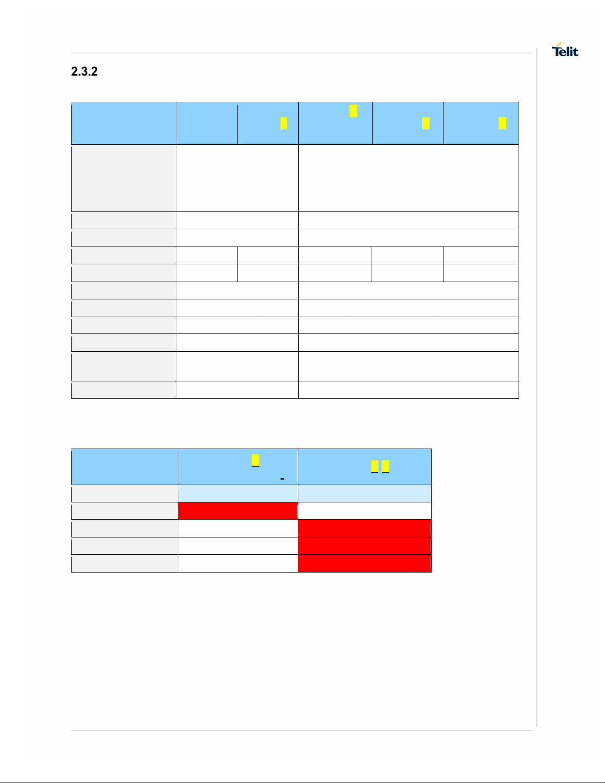
Product Variants
The SL871 family includes the following variants:
• SL871 – Flash memory based, Multi-constellation
• SL871 (Gen 1): EOL in July 2015
• SL871 (Gen 2): Switching Mode Power Supply;
Added Antenna On, Antenna Sense, and Force On pins
• SL871L: Added an LNA and DC blocking capacitor
• SL871-S – ROM based, GPS-only
• SL871-S: Switching Mode Power Supply and Antenna On pin
• SL871 L-S: Added an LNA and DC blocking capacitor
SL871-S and SL871L-S Features
• GPS-only
• ROM-based (Firmware cannot be updated)
• The 2
• Locally generated AGPS (EASY - Embedded Assist System) on SL871-S and SL871L-S
• Server-generated AGPS (EPO - Extended Prediction Orbit) is supported via a host
2.3.1.1. ROM versions
The current SL871-S and SL871L-S have the MT3337E (enhanced) ROM with the following
changes -
Added features:
Deleted features:
nd
port is UART only (I2C is not supported)
is supported only on MT3337E ROM (version 2.3) after Oct. 2015.
Earlier ROM versions did not support EASY.
system for the SL871-S and SL871L-S.
Please refer to the MT333x Host EPO Application Note
• Improved TTFF and Position,
• EASY
• PPS sync with NMEA
• SBAS
• Always Locate
• LOCUS
1VV0301170 Rev. 6 Page 14 of 85 2018-03-13
Page 15
SL871 Family Product User Guide PRODUCT DESCRIPTION
SL871-S
Production)
GPS
Galileo
GPS
Memory
Flash
ROM
Power Supply
Switching
Switching
Internal LNA
No
Yes
No
No
Yes
DC blocking cap
No
Yes
No
No
Yes
2nd Port
Yes (UART / I2C)
Yes (UART only)
Antenna Sense
Yes
No
Antenna On
Yes
Yes
Force On
Yes
No
Software
Upgradable
Yes
No
EPO
Yes
Yes (host)
ROM version
3337
3337E (enhanced)
EASY
No
Yes
SBAS
Yes
No
AlwaysLocate
Yes
No
LOCUS
Yes
No
SL871 Product Features Table
Feature SL871 SL871L
Constellations
Supported
QZSS
Glonass
BeiDou
(Early
SL871-S SL871L-S
QZSS
Table 2-1 SL871 Family Product Features
Feature
SL871-S
(early production)
Table 2-2 ROM Features (-S modules only)
SL871L-S
1VV0301170 Rev. 6 Page 15 of 85 2018-03-13
Page 16
SL871 Family Product User Guide PRODUCT DESCRIPTION
Block Diagrams
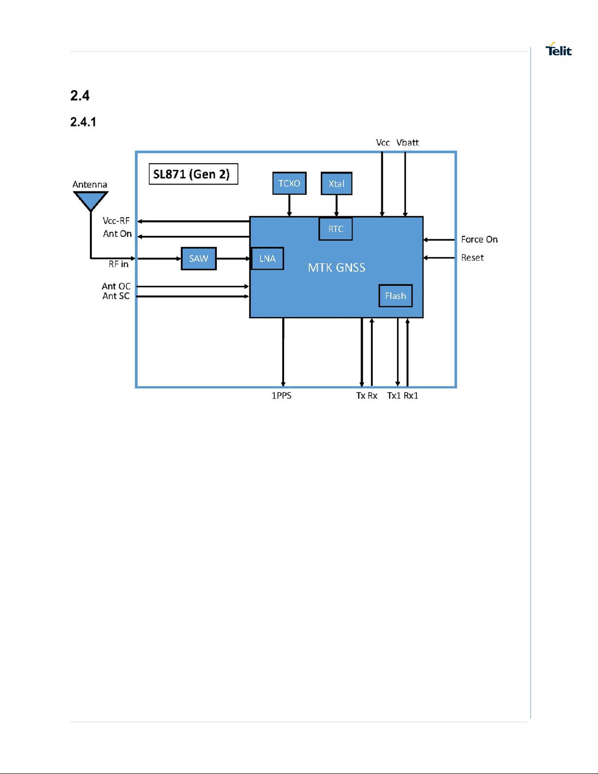
SL871 (Gen 2) Block Diagram
Figure 2-1 SL871 (Gen 2) Block Diagram
1VV0301170 Rev. 6 Page 16 of 85 2018-03-13
Page 17
SL871 Family Product User Guide PRODUCT DESCRIPTION
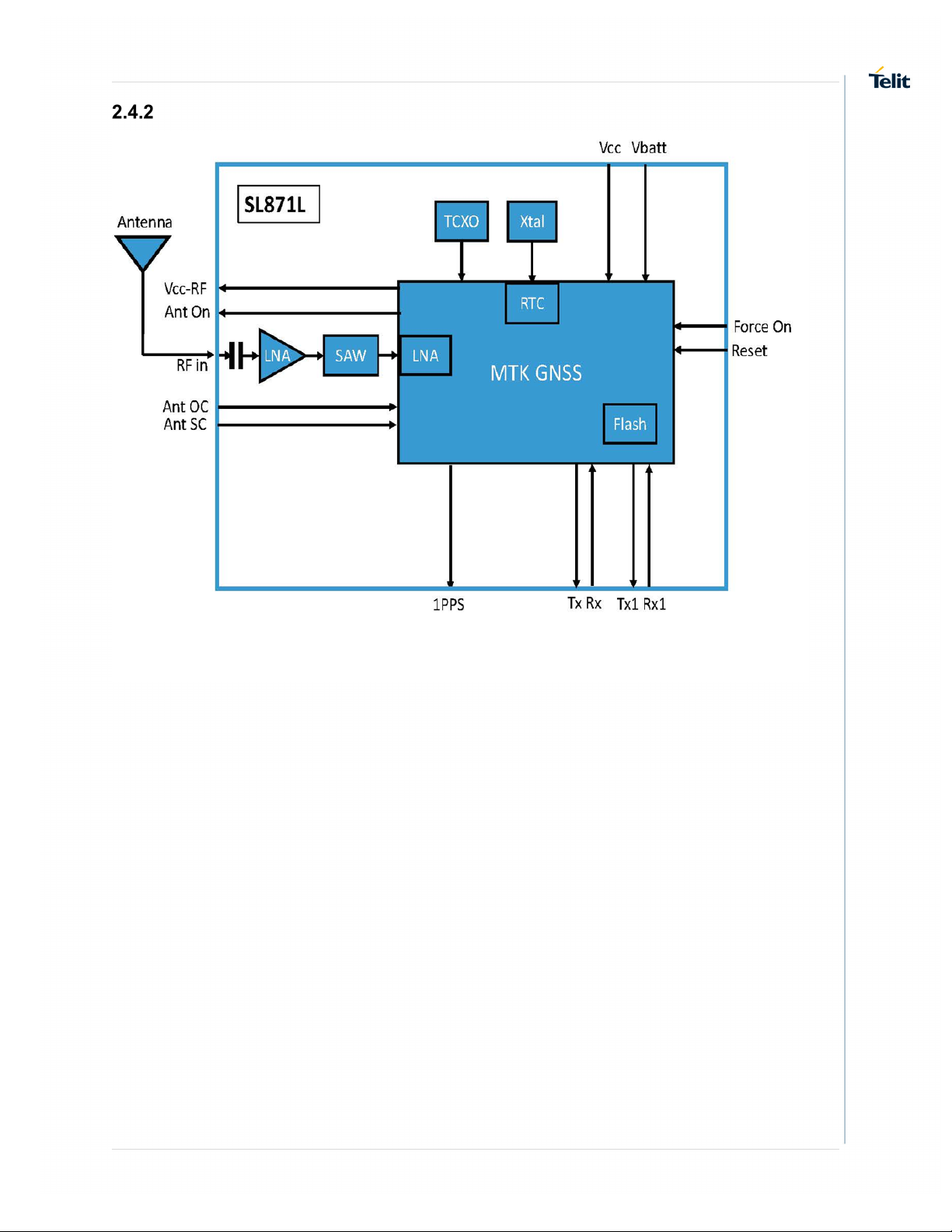
SL871L Block Diagram
Figure 2-2 SL871L Block Diagram
1VV0301170 Rev. 6 Page 17 of 85 2018-03-13
Page 18
SL871 Family Product User Guide PRODUCT DESCRIPTION
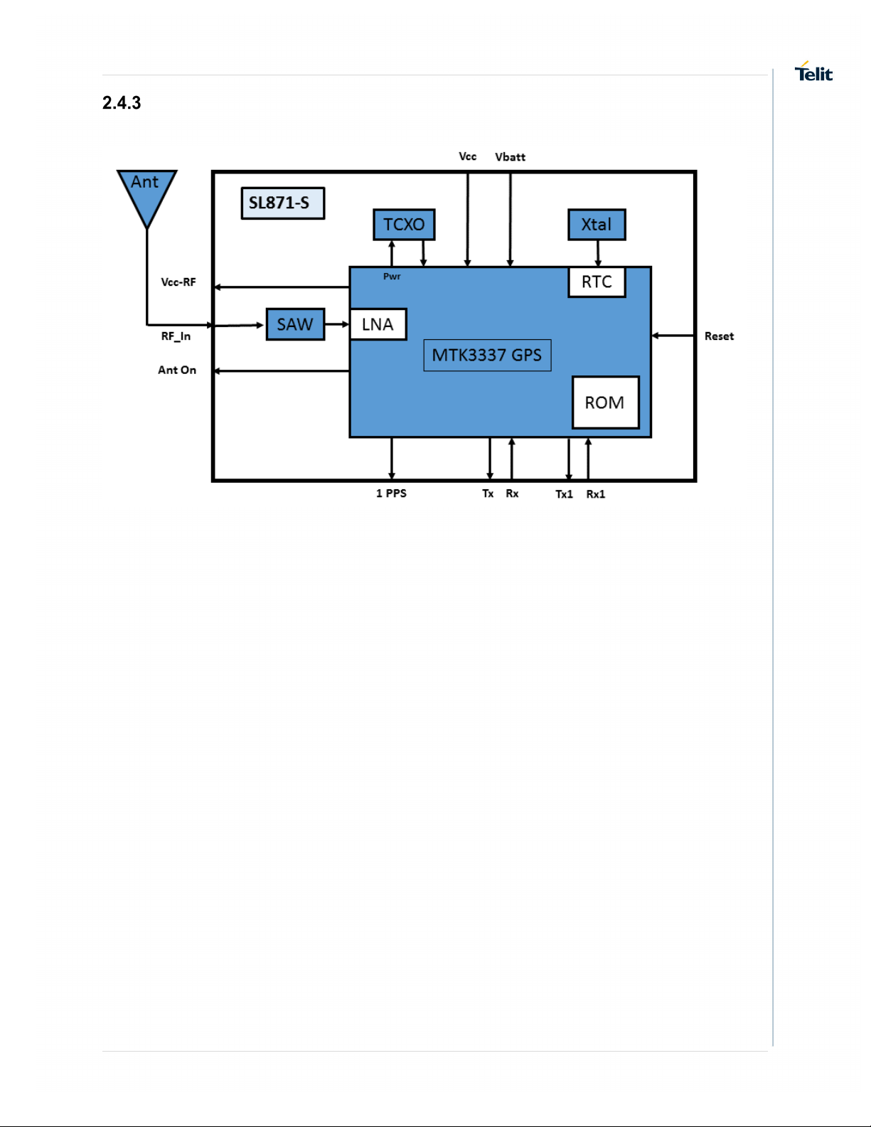
SL871-S Block Diagram
Figure 2-3 SL871-S - Block Diagram
1VV0301170 Rev. 6 Page 18 of 85 2018-03-13
Page 19
SL871 Family Product User Guide PRODUCT DESCRIPTION
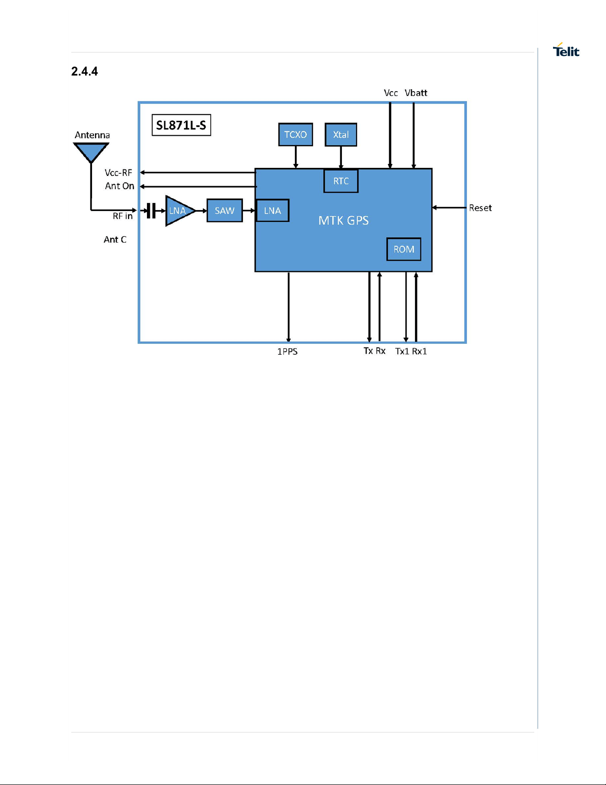
SL871L-S Block Diagram
Figure 2-4 SL871L-S - Block Diagram
1VV0301170 Rev. 6 Page 19 of 85 2018-03-13
Page 20
SL871 Family Product User Guide PRODUCT DESCRIPTION
Module Photo
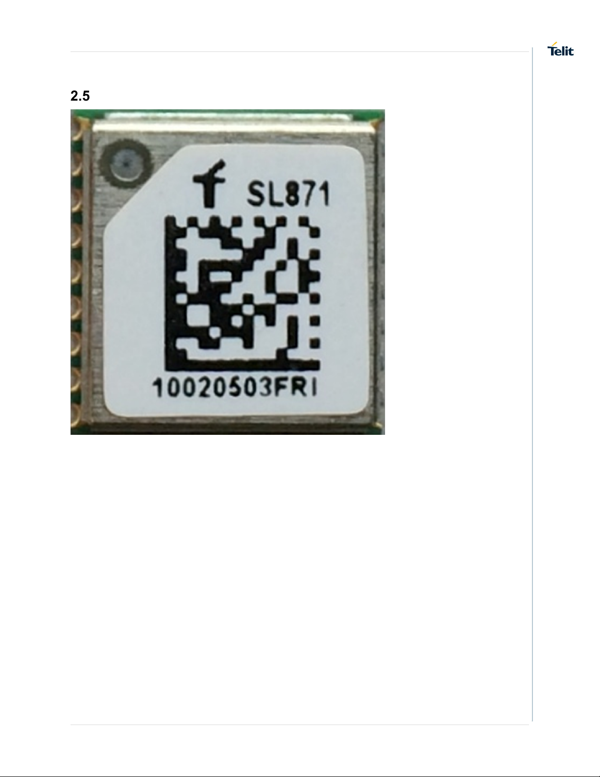
Figure 2-5 SL871 Family Module – Photo
Note: All variants have similar appearance (except for the product name).
1VV0301170 Rev. 6 Page 20 of 85 2018-03-13
Page 21
SL871 Family Product User Guide EVALUATION KIT
3 EVALUATION KIT
Please refer to the product Evaluation Kit User Guide for detailed information.
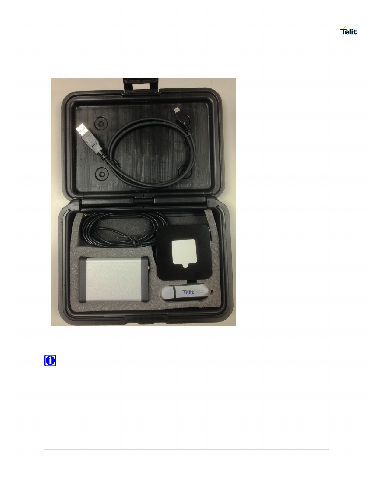
Figure 3-1 Evaluation Kit contents
Note: The SL871 kit includes a GPS / GLONASS / BeiDou antenna.
1VV0301170 Rev. 6 Page 21 of 85 2018-03-13
Page 22
SL871 Family Product User Guide EVALUATION KIT
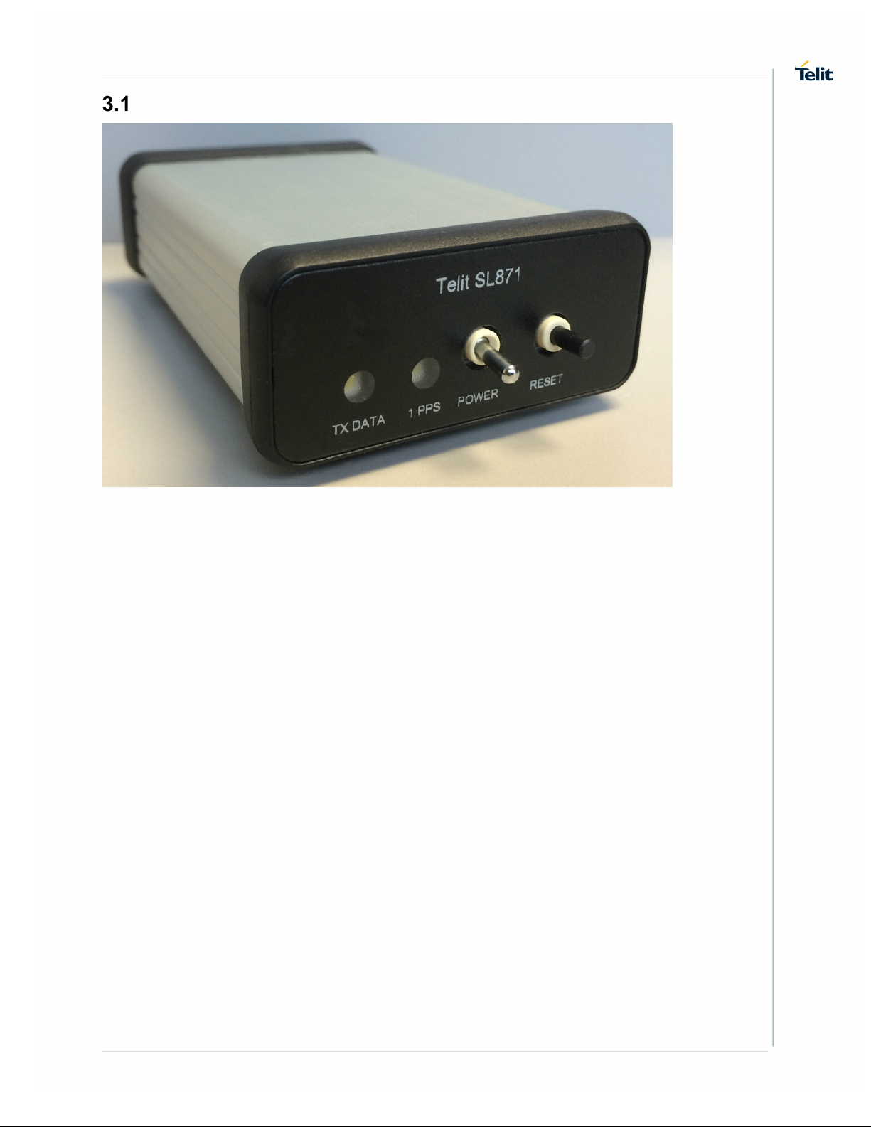
Evaluation Unit
Figure 3-2 SL871 Evaluation Unit
1VV0301170 Rev. 6 Page 22 of 85 2018-03-13
Page 23

SL871 Family Product User Guide PRODUCT FEATURES
4 PRODUCT FEATURES
Multi-Constellation Navigation (SL871 and SL871L only)
GPS and GLONASS constellations are enabled by default.
The user may enable or disable constellations via the $PMTK353 command
The SL871-S and SL871L–S support GPS only.
Quasi-Zenith Satellite System (QZSS)
The satellites of the Japanese regional SBAS are in a highly inclined, elliptical geosynchronous
orbit, allowing continuous high-elevation coverage over Japan using only three satellites plus
one geostationary satellite. They provide ranging signals, but also may be used for
augmentation of the GPS system.
QZSS constellation usage is controlled by the $PMTK352 command and is disabled by default.
NMEA reporting for QZSS may be enabled/disabled by the $PMTK351 command.
Satellite-Based Augmentation System (SBAS)
SBAS is not supported on the current production SL871-S modules (with the enhanced ROM).
The receiver is capable of using SBAS satellites as a source of both differential corrections and
satellite ranging measurements. These systems (WAAS, EGNOS, GAGAN and MSAS) use
geostationary satellites to transmit signals similar to those of GPS in the same L1 band.
Enabling the SBAS feature limits the maximum fix rate to 5 Hz. If disabled, the maximum is 10
Hz (except for SL871-S modules).
The module is enabled for SBAS by default, but can be disabled by command $PTMK313.
Either SBAS or DGPS corrections can be used and are set by the $PMTK301 command.
SBAS Corrections
The SBAS satellites transmit a set of differential corrections to their respective regions. The use
of SBAS corrections can improve positioning accuracy.
SBAS Ranging
The use of SBAS satellites can augment the number of measurements available for the
navigation solution, thus improving availability and accuracy.
Differential GPS (DGPS) (SL871 and SL871L only)
DGPS is a Ground-Based Augmentation System (GBAS) for reducing position errors by
applying corrections from a set of accurately-surveyed ground stations located over a wide
area. These reference stations measure the range to each satellite and compare it to the
known-good range. The differences can then be used to compute a set of corrections which are
transmitted either by radio to a DGPS receiver or over the internet.
The DGPS receiver can then send them to serial port 2 (RX1) using the RTCM SC-104 protocol
message types 1, 2, 3, and 9.
These corrections can significantly improve the accuracy of the position reported to the user.
The receiver can accept either the RTCM SC-104 messages or SBAS differential data via
command $PMTK501. .
1VV0301170 Rev. 6 Page 23 of 85 2018-03-13
Page 24

SL871 Family Product User Guide PRODUCT FEATURES
Assisted GPS (AGPS)
Assisted GPS (or Aided GPS) is a method by which information from a source other than
broadcast GPS signals is used to improve (i.e. reduce) TTFF.
The necessary ephemeris data is calculated either by the receiver itself (locally-generated
ephemeris), or a server (server-generated ephemeris) and is then stored in the module.
See Section 2.3 Product Variants for applicability.
Locally-generated AGPS - Embedded Assist System (EASY)
This feature is not supported on the SL871-S until ROM MT3337E version (enhanced) of Oct
2015. It is supported on the SL871L-S.
Proprietary algorithms within the module perform GPS ephemeris prediction locally from stored
broadcast ephemeris data (received from tracked satellites). The algorithms predict orbital
parameters for up to three days. The module must operate in Full Power mode for at least 5
minutes to collect ephemeris data from visible satellites, or 12 hours for the full constellation.
EASY is disabled if the fix rate is > 1 Hz
EASY is on by default, but can be disabled by command PMTK869.
Server-generated AGPS - Extended Prediction Orbit (EPO)
(SL871 and SL871L only)
Server-generated ephemeris predictions are maintained on Telit AGPS servers. The predicted
ephemeris file is obtained from the AGPS server and is transmitted to the module over serial
port 1 (RX). These predictions do not require local broadcast ephemeris collection, and are valid
for up to 14 days.
Note that the EPO data stream does not conform to the NMEA-0183 standard.
Please refer to the Telit EPO Application Note for details.
Example source code is available under NDA.
Contact TELIT for support regarding this service.
See the next section regarding EPO support (Host EPO) on the SL871-S and SL871L-S.
Host EPO
The SL871-S and SL871L-S do not have flash memory. However, they can still make use of
Assisted GPS. If the system design includes a host processor, it can access server-generated
EPO data and send it to the module over the primary serial port. This data is valid for six hours.
Host EPO data is not retained over a power cycle.
Note that the EPO data stream does not conform to the NMEA-0183 standard.
Please refer to the MT333x Host EPO Application Note.
Please contact Telit support for further details.
10 Hz Navigation
The default rate of 1 Hz can be changed by command $PMTK500 to a maximum of 10 Hz.
Enabling the SBAS feature limits the maximum fix rate to 5 Hz.
The SL871-S and SL871L-S maximum is 5 Hz.
Elevation Mask Angle
The default elevation mask angle is 5°. It can be changed via the PMTK311 command.
1VV0301170 Rev. 6 Page 24 of 85 2018-03-13
Page 25
SL871 Family Product User Guide PRODUCT FEATURES
Static Navigation
Static Navigation is an operating mode in which the receiver will freeze the position fix when the
speed falls below a set threshold (indicating that the receiver is stationary).
The course and altitude are also frozen, and the speed is reported as “0”.
The navigation solution is unfrozen when the speed increases above a threshold or when the
computed position exceeds a set distance (10 m) from the frozen position (indicating that the
receiver is again in motion). The speed threshold can be set via the command.
Set this threshold to zero to disable static navigation.
This feature is useful for applications in which very low dynamics are not expected, the classic
example being an automotive application.
Static Navigation is disabled by default, but can be enabled by command $PMTK386.
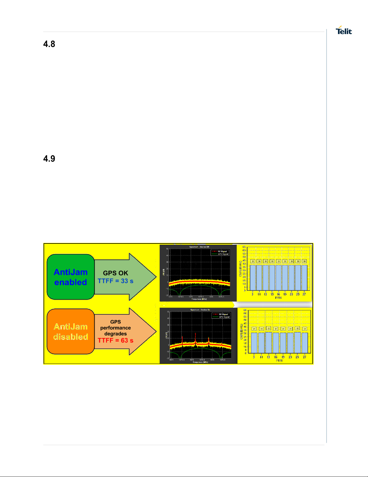
Jamming Rejection – Active Interference Cancellation (AIC)
The receiver module detects and removes narrow-band interfering signals (jamming signals)
without the need for external components or tuning. It rejects up to 12 CW (Continuous Wave)
type signals of up to –80 dBm (total power signal levels). This feature is useful both in the
design stage and during the production stage for uncovering issues related to unexpected
jamming. When enabled, Jamming Rejection will increase current drain by about 1 mA, and
impact on GNSS performance is low at modest jamming levels. However, at high jamming
levels (e. g. –90 to –80 dBm), the RF signal sampling ADC starts to become saturated after
which the GNSS signal levels start to diminish.
Jamming rejection is enabled by default, but can be disabled with the PMTK286 command.
Figure 4-1Jamming Rejection
1VV0301170 Rev. 6 Page 25 of 85 2018-03-13
Page 26

SL871 Family Product User Guide PRODUCT FEATURES
Internal LNA (SL871L and SL871L-S only)
The SL871L and SL871L-S modules include a built-in LNA to improve sensitivity.
1PPS
The module provides a 1PPS output signal. See Section 9.3.4.1 1PPS for details.
1VV0301170 Rev. 6 Page 26 of 85 2018-03-13
Page 27

SL871 Family Product User Guide PRODUCT FEATURES
Power Management Modes
The receiver supports operating modes that reduce overall current consumption with less
frequent position fixes. Availability of GNSS signals in the operating environment will be a factor
in choosing power management modes. The designer can choose a mode that provides the
best trade-off of navigation performance versus power consumption.
The various power management modes can be enabled by sending the desired command using
the host serial port (RX).
Table 4-1 Power Management - Command summary
Full Power Continuous Mode
The module starts in full power continuous mode when powered up. This mode uses the
acquisition engine to search for all possible satellites at full performance, resulting in the highest
sensitivity and the shortest possible TTFF.
The receiver then switches to the tracking engine to lower the power consumption when:
• A valid GPS/GNSS position is obtained
• The ephemeris for each satellite in view is valid
To return to Full Power mode from a low power mode, send a $PMTK225,0*2B
command just after the module wakes up from its previous sleep cycle.
If power is removed from both Vcc and Vbatt, then Time, Ephemeris, Almanac, EASY, EPO
data, and PMTK configuration data will be lost. If Vbatt is present, no data will be lost.
1VV0301170 Rev. 6 Page 27 of 85 2018-03-13
Page 28

SL871 Family Product User Guide PRODUCT FEATURES
Backup Mode (Perpetual) (SL871 and SL871L only)
In the backup mode, the internal Power Management Unit is turned off, leaving only BBRAM
and the RTC powered up. This reduces power consumption to the minimum required that still
provides data retention to enable hot and warm starts.
To enter the Perpetual Backup mode, use the NMEA command: $PMTK225,4.
Only the SL871 and SL871L have a Force_On pin.
This command will be rejected on the other modules (SL871-S and SL871L-S).
To exit the Perpetual Backup mode, bring the Force_On signal high, then return to low. See
Section 9.3.3.2 FORCE-ON for details.
Standby Modes
In these modes the receiver stops navigation, the internal processor enters the standby state,
and the current drain at main supply VCC_IN is substantially reduced.
STOP: ARM baseband, RF, and TCXO are powered down
SLEEP: ARM baseband and RF are powered down
To enter a Standby mode, send the following command:
$PMTK161,0*28 (STOP Mode)
$PMTK161,1*29 (SLEEP Mode)
To exit a Standby mode, send any byte to the host port (RX).
GLP Mode (SL871 and SL871L modules only)
In the GNSS Low Power (GLP) mode, power consumption is reduced for some time during a
one second period. The module will alternate this cycling with periods of full power when
necessary, for example weak signals or decoding the navigation message.
A typical current draw is 10 to 14 mA, depending on conditions.
Note that positon accuracy will be reduced during GLP operation, therefore the user must
determine the tradeoff between power consumption and desired accuracy.
A timeline is shown below:
Figure 4-2 GNSS Low Power (GLP) mode diagram
To enter the GLP mode, send the command:
$PMTK262,3
To exit the GLP mode and return to full-power mode, send the command:
$PMTK262,0
1VV0301170 Rev. 6 Page 28 of 85 2018-03-13
Page 29

SL871 Family Product User Guide PRODUCT FEATURES
Periodic Modes (SL871 and LS871L only)
These modes allow autonomous power on/off control with reduced fix rate to decrease average
power consumption. The main power supply pin VCC_ON is still powered, but power distribution
to internal circuits is internally controlled by the receiver.
STANDBY(SLEEP): ARM baseband and RF are powered down.
BACKUP: ARM baseband, RF, and TCXO are powered down. RTC is powered up.
Figure 4-3 Periodic Modes diagram
Figure 4-4 Periodic Mode example 1
Figure 4-5 Periodic Mode example 2
1VV0301170 Rev. 6 Page 29 of 85 2018-03-13
Page 30

SL871 Family Product User Guide PRODUCT FEATURES
To enter a Periodic mode, send the following NMEA command(s):
$PMTK223
Where:
SV = 1 to 4, default = 1
SNR = 25 to 30, default = 28
Ext. threshold = 40 000 to 180 000 ms, default = 180 000
Ext. gap = 0 to 3 600 000 ms, default = 180 000
This is the limit between successive DEE
$PMTK225
Where:
Example: $PMTK225,1,3000,12000,18000,72000*16
for periodic mode with 3 s navigation and 12 s sleep in backup state.
The acknowledgement response for the command is:
$PMTK001,225,3*35
To exit Periodic Sleep mode, send the NMEA command
$PMTK225,0*2B
just after the module wakes up from a previous sleep cycle.
,<SV>,<SNR>,<Extension threshold>,<Extension gap>*<checkum> (Optional)
,<Type>,<Run_time>,<Sleep_time>,<2nd_run_time>,<2nd_sleep_time>*<checkum>
Type = 1 for Periodic (backup) mode or 2 for Periodic (standby) mode
Run_time = Full Power period (ms)
Sleep_time = Standby period (ms)
nd
2
_run_time = Full Power period (ms) for extended acquisition if GNSS acquisition fails
during Run_time
nd
2
_sleep_time = Standby period (ms) for extended sleep if GNSS acquisition fails during
Run_time
AlwaysLocate™ Modes
(Not available on the SL871L-S and current production SL871-S with enhanced ROM)
AlwaysLocate™ is an intelligent controller of the Periodic mode where the main supply pin
VCC_IN is still powered, but power distribution is controlled internally. Depending on the
environment and motion conditions, the module can autonomously and adaptively adjust the
parameters of the Periodic mode, e.g. RF on/off ratio and fix rate, to achieve a balance in
positioning accuracy and power consumption. The average current drain will vary based on
conditions.
To enter an AlwaysLocate mode, send the following NMEA command:
$PMTK225,<mode>*<checksum><CR><LF>
Where mode = 8 for AlwaysLocate (standby) mode or 9 for AlwaysLocate (backup) mode
Example: $PMTK225,9*22
The acknowledgement response for the command is:
$PMTK001,225,3*35
To exit AlwaysLocate mode, send the NMEA command:
$PMTK225,0*2B
just after the module wakes up from its previous sleep cycle.
1VV0301170 Rev. 6 Page 30 of 85 2018-03-13
Page 31

SL871 Family Product User Guide DATA RETENTION
Data Retention (1)
Initialization
Almanac
Ephemeris
EPO
Host EPO
EASY
Position
Time
Power Cycle
Y (2)
Reset (signal)
Y
Full Cold
Start
Cold Start
Y Y Y Y (3)
Warm Start
Y Y Y Y Y Y
Hot Start
Y Y Y Y Y Y Y
Reacquisition
Y Y Y Y Y Y Y
Note 1: Commanded parameters (e.g. UART speed, feature enables, etc.) are not
preserved over a power cycle.
Note 2: EPO is not available on the MT3337 (ROM)-based modules. Use Host EPO.
Note 3: The standard definition of “Cold Start” does not allow time to be preserved.
Use “Full Cold Start” to compare with other vendor’s products’ “Cold Start”.
5 DATA RETENTION
(SL871 and SL871L modules only)
The receiver is capable of retaining data elements under the various initialization types.
If Vbatt is maintained, no data will be lost.
The following table shows which data elements are saved under each type of initialization if both
Vcc and Vbatt are removed.
To erase EPO data, use the $PMTK127 command.
Y (3)
Table 5-1 Data Retention
1VV0301170 Rev. 6 Page 31 of 85 2018-03-13
Page 32

SL871 Family Product User Guide PRODUCT PERFORMANCE
Horizontal Position Accuracy
Constellation(s)
CEP (m)
GPS
2.5
Glonass
2.6
BeiDou
10.2
GPS + Glonass
2.5
GPS + BeiDou
2.5
Test Conditions: 24-hr Static, -130 dBm, Full Power mode.
6 PRODUCT PERFORMANCE
Performance - SL871 and SL871L
Earlier variants have different performance values.
Horizontal Position Accuracy - SL871 and SL871L
Table 6-1 SL871 and SL871L Horizontal Position Accuracy
1VV0301170 Rev. 6 Page 32 of 85 2018-03-13
Page 33

SL871 Family Product User Guide PRODUCT PERFORMANCE
Constellation(s)
Start Type
Max TTFF (s)
Hot
1
Warm Assisted
2.4
Warm
32
Cold
33
Hot
1.4
Warm Assisted
2.4
Warm
32
Cold
33
Hot
1.5
Warm
35
Cold
46
Hot
1
Warm Assisted
2.4
Warm
28
Cold
31
Hot
1
Warm
32
Cold
33
Test Conditions: Static scenario, -130 dBm, Full Power mode
Time to First Fix - SL871 and SL871L
GPS
Glonass
BeiDou
GPS + GLO
GPS + BeiDou
Table 6-2 SL871 and SL871L Time to First Fix
1VV0301170 Rev. 6 Page 33 of 85 2018-03-13
Page 34

SL871 Family Product User Guide PRODUCT PERFORMANCE
Constellation(s)
State
Minimum Signal Level (dBm)
SL871 (Gen 2)
SL871L
Acquisition
-145
-147
Navigation
-159
-160
Tracking
-162
-163
Acquisition
-144
-146
Navigation
-156
-159
Tracking
-158
-161
Acquisition
-143
-146
Navigation
-156
-159
Tracking
-158
-162
Sensitivity - SL871 (Gen 2) and SL871L
GPS
GLONASS
BeiDou
Note: The above performance values were measured under ideal lab
conditions using a GNSS simulator generating a static scenario.
Table 6-3 SL871 (Gen 2) and SL871L Receiver Sensitivity
1VV0301170 Rev. 6 Page 34 of 85 2018-03-13
Page 35

SL871 Family Product User Guide PRODUCT PERFORMANCE
Parameter
Constellation
CEP (m)
Horizontal Position Accuracy
GPS
2.5
Test Conditions: 24-hr Static, -130 dBm, Full Power mode
Constellation
Start Type
Max TTFF (s)
Hot
1
Warm Assisted
2.4
Warm
32
Cold
33
Test Conditions: -130 dBm, Full Power mode, Static scenario
Constellation
State
Minimum Signal Level (dBm)
SL871-S
Gen 2
SL871L-S
Acquisition
-144
-147
Navigation
-159
-161
Tracking
-163
-164
Performance - SL871-S and SL871L-S
Position Accuracy - SL871-S and SL871L-S
Table 6-4 SL871-S and SL871L-S Position Accuracy
Time to First Fix - SL871-S and SL871L-S
GPS
Table 6-5 SL871-S and SL871L-S Time to First Fix
Sensitivity - SL871-S and SL871L-S
GPS
Note: The above performance values were measured under ideal lab
conditions using a GNSS simulator generating a static scenario.
Table 6-6 SL871-S and SL871L-S Sensitivity
1VV0301170 Rev. 6 Page 35 of 85 2018-03-13
Page 36

SL871 Family Product User Guide PRODUCT PERFORMANCE
Jamming Mitigation Performance example
Figure 6-1 Jamming with AIC Disabled
Figure 6-2 Jamming with AIC Enabled
1VV0301170 Rev. 6 Page 36 of 85 2018-03-13
Page 37

SL871 Family Product User Guide SOFTWARE INTERFACE
Message ID
Description
RMC
GNSS Recommended minimum navigation data
GGA
GNSS position fix data
GSA
GNSS Dilution of Precision (DOP) and active satellites
GSV
GNSS satellites in view.
Message
Description
GLL
Geographic Position – Latitude & Longitude
VTG
Course Over Ground & Ground Speed
ZDA
Time & Date
7 SOFTWARE INTERFACE
Serial I/O port 1 (RX and TX pins) supports full duplex communication between the receiver and
the user.
The default serial configuration is: NMEA, 9600 bps, 8 data bits, no parity, 1 stop bit.
More information regarding the software interface can be found in the Telit MT Software User
Guide.
Customers that have executed a Non-Disclosure Agreement (NDA) with Telit may obtain
the Telit MT-GNSS Authorized Software User Guide, which contains additional
proprietary information.
NMEA Output Messages
Some sentences may exceed the NMEA length limitation of 80 characters.
Default: GPS constellation enabled.
GLONASS is also enabled for SL871 and SL871L.
Default fix rate: 1 Hz. Maximum rate is 10 Hz.
Note: Multiple GSA and GSV messages may be output on each cycle.
Standard Messages
Table 7-1 Default NMEA output messages
The following messages can be enabled by command:
Table 7-2 Available Messages
1VV0301170 Rev. 6 Page 37 of 85 2018-03-13
Page 38

SL871 Family Product User Guide SOFTWARE INTERFACE
Talker ID
Constellation
BD
BeiDou
GA
Galileo
GL
GLONASS
GP
GPS
QZ
QZSS
The following table shows the Talker IDs used:
Table 7-3 NMEA Talker IDs
Proprietary Output Messages
The modules support several proprietary NMEA output messages which report additional
receiver data and status information.
Message ID Description
$PMTK010 System messages (e.g. to report startup, etc.)
Table 7-4 Proprietary Output Messages
1VV0301170 Rev. 6 Page 38 of 85 2018-03-13
Page 39

SL871 Family Product User Guide SOFTWARE INTERFACE
Command
Description
Test. This command will be echoed back to the sender
(for testing the communications link).
$PMTK101
Perform a HOT start
$PMTK102
Perform a WARM start
$PMTK103
Perform a COLD start. However, time is preserved.
Perform a system reset (erasing any stored almanac
data) and then a COLD start
$PMTK120
Erase aiding data stored in flash memory
$PMTK127
Erase EPO data stored in flash memory
$PMTK251,Baudrate
Set NMEA Baud rate
$PMTK313,0
Disable SBAS feature
$PMTK313,1
Enable SBAS feature
$PMTK353,1,0,0,0,0
Enable GPS only mode
$PMTK353,0,1,0,0,0
Enable GLO only mode
$PMTK353,0,0,0,0,1
Enable BDS only mode
$PMTK353,1,1,0,0,0
Enable GPS and GLO mode
$PMTK353,1,0,0,0,1
Enable GPS and BDS mode
NOTE: Multi-constellation commands are not supported by the SL871-S modules
NMEA Input Commands
The modules use NMEA proprietary messages for commands and command responses. This
interface provides configuration and control over selected firmware features and operational
properties of the module. Wait time is about 50 to 100 ms.
The format of a command is: $<command-ID>[,<parameters>]*<cr><lf>
Commands are NMEA proprietary format and begin with “$PMTKxxx”.
Parameters, if present, are comma-delimited as specified in the NMEA protocol.
Unless otherwise noted in the Software User Guide, commands are echoed back to the user
after the command is executed.
NMEA Commands List
See Table 4-1 Power Management - Command summary for power management
commands.
$PMTK000
$PMTK104
Table 7-5 NMEA Input Commands
1VV0301170 Rev. 6 Page 39 of 85 2018-03-13
Page 40

SL871 Family Product User Guide FLASH UPGRADABILITY
8 FLASH UPGRADABILITY
(SL871 and SL871L only)
Note: The SL871-S and SL871L-S have ROM and are not upgradable.
Please refer to the product EVK User Guide for more detailed information.
The firmware stored in the internal Flash memory of the SL871 may be upgraded via the serial
port TX/RX pins. In order to update the FW, the following steps should be performed to reprogram the module.
1. Remove all power to the module.
2. Connect serial port USB cable to a PC.
3. Apply main power.
4. Clearing the entire flash memory is strongly recommended prior to programming.
5. Run the software utility to re-flash the module.
6. Upon successful completion of re-flashing, remove main power to the module for a
minimum of 10 seconds.
7. Apply main power to the module.
8. Verify the module has returned to the normal operating state.
1VV0301170 Rev. 6 Page 40 of 85 2018-03-13
Page 41

SL871 Family Product User Guide ELECTRICAL INTERFACE
9 ELECTRICAL INTERFACE
Pinout diagrams and tables
SL871 (Gen 2) and SL871L Pin-out diagram and table
Figure 9-1 SL871 (Gen 2) and SL871L Pin-out diagram
1VV0301170 Rev. 6 Page 41 of 85 2018-03-13
Page 42

SL871 Family Product User Guide ELECTRICAL INTERFACE
1
GND
GND
Ground
2
TX O TX0. See 9.4.2 UART Port Operation.
3
RX I RX0. See 9.4.2 UART Port Operation.
4
1PPS
O
Time mark Pulse, (1PPS). See 9.3.4.1 1PPS
Antenna-Open (high true). See 9.3.2.3 ANT-OC
(SL871 and SL871L only)
6
VBATT
PWR
Backup Voltage Supply. See 9.2 DC Power Supply
Can be connected to VCC (for compatibility)
or left unconnected.
8
VCC
PWR
Supply Voltage. See 9.2 DC Power Supply
RESET-N (Active Low, open drain) May be left
unconnected. See 9.3.3.1 RESET-N
10
GND
GND
Ground
Max DC voltage: ± 3.0 V (Gen 2)
12
GND
GND
Ground
13
ANT-ON
O
Antenna On. See 9.3.2.2 ANT-ON (output)
9.3.2.1 VCC-RF (Active Antenna Supply Voltage)
Antenna Shorted (low true). See 9.3.2.4 ANT-SC-N
(SL871 and SL871L only)
TX1 / SDA. See 9.4.3 I2C Port Operation
(SL871 and SL871L only)
RX1 / SCL. See 9.4.3 I2C Port Operation
(SL871 and SL871L only)
18
FORCE-ON-N
I
FORCE ON. See 9.3.3.2 FORCE-ON
Notes:
All GND pins must be connected to ground.
Pin Name Type Description Notes
5 ANT-OC I
7 NC NC
9 RESET-N I
11 RF-IN I
14 VCC-RF PWR
GNSS RF Input. 50 Ω. See 9.5 Antenna RF Interface
Output Voltage for a bias-T (max 50 mA).
See
1
15 ANT-SC-N I
16 SDA / TX1 I/O
17 SCL / RX1 I/O
1. DC Blocking capacitor has been added in SL871L.
2. UART on Port 1 (pins 16 &17) requires a custom software build.
Table 9-1 SL871 (Gen 2) & SL871L Pin-out Table
1VV0301170 Rev. 6 Page 42 of 85 2018-03-13
2
2
Page 43

SL871 Family Product User Guide ELECTRICAL INTERFACE
SL871-S and SL871L-S Pin-out diagram and table
Figure 9-2 SL871-S and SL871L-S Pin-out diagram
1VV0301170 Rev. 6 Page 43 of 85 2018-03-13
Page 44

SL871 Family Product User Guide ELECTRICAL INTERFACE
1
GND
GND
Ground
2
TX O TX0. See 9.4.2 UART Port Operation.
3
RX I RX0. See 9.4.2 UART Port Operation.
4
1PPS
O
Time mark Pulse, (1PPS). See 9.3.4.1 1PPS
5
NC
NC
No Connection
6
VBATT
PWR
Backup Voltage Supply. See 9.2 DC Power Supply
Can be connected to VCC (for
compatibility) or left unconnected
8
VCC
PWR
Supply Voltage. See 9.2 DC Power Supply
RESET-N (Active Low, open drain). May be
left unconnected. See 9.3.3.1 RESET-N
10
GND
GND
Ground
GNSS RF Input. 50 Ω. See 9.5 Antenna RF Interface
Max DC voltage: ± 3.0 V (Gen 2)
12
GND
GND
Ground
13
ANT-ON
O
Antenna On. See 9.3.2.2 ANT-ON (output)
15
NC
NC
No Connection
16
TX1 O TX1 See 9.4.2 UART Port Operation..
17
RX1 I RX1. See 9.4.2 UART Port Operation..
18
NC
NC
No Connection
Note 1. DC Blocking capacitor has been added in SL871L-S.
All GND pins must be connected to ground.
Pin Name Type Description Notes
7 NC NC
9 RESET-N I
11 RF-IN I
14 VCC-RF PWR
Output Voltage for a bias-T (max 50 mA).
See 9.3.2.1 VCC-RF (Active Antenna Supply Voltage)
1
Table 9-2 SL871-S & SL871L-S Pin-out Table
1VV0301170 Rev. 6 Page 44 of 85 2018-03-13
Page 45

SL871 Family Product User Guide ELECTRICAL INTERFACE
DC Power Supply
The modules have two power supply pins Vcc and Vbatt.
Note that I/O voltage ranges are different from supply voltages V
and V
CC
BATT
.
An external LDO without a fast discharge output feature must be used.
VCC
This is the main power input. The supply voltage must be in the range specified in Table 9-3 DC
Supply Voltage below.
Vcc does not supply the RTC domain, therefore Vbatt must be supplied (externally) any
time that Vcc is powered up. This may be accomplished by tying VBATT to VCC.
When power is first applied, the module will start up in full power continuous operation mode.
During operation, the current drawn by the module can vary greatly, especially if enabling lowpower operation modes. The supply must be able to handle the current fluctuation including any
inrush surge current.
GPS/GNSS receiver modules require a clean and stable power supply. In designing such a
supply, any resistance in the Vcc line can negatively influence performance. Consider the
following points: All supplies should be within the rated requirements. At the module input, use
low ESR capacitors that can deliver the required current for switching from backup mode to
normal operation. Keep the rail short and away from any noisy data lines or switching supplies,
etc. Wide power lines and power planes are preferred.
VBATT
Battery backup power input (as specified in the table below) must be supplied any time
Vbatt may be directly connected to a lithium coin cell (2.8 to 4.3 V).
Vbatt supplies power to the following elements (the RTC domain):
This allows the module to retain time and ephemeris information, thus enabling hot and warm
starts, which will improve TTFF.
that Vcc is powered up.
• real-time clock (RTC)
• battery backed RAM (BBRAM)
• EASY data
• Persistent data elements (not commanded option values).
VCC_RF
VCC_RF is directly connected to VCC internally and may be used to power an external LNA or
bias-T. Maximum current available is 50 mA. It may be left unconnected.
1VV0301170 Rev. 6 Page 45 of 85 2018-03-13
Page 46

SL871 Family Product User Guide ELECTRICAL INTERFACE
Main Supply Voltage & Backup Voltage
Supply
Name
Min
Typ
Max
Units
State & Constellation
Typ
Max
Units
Acquisition
GPS Only
61
88
mW
GPS and Glonass
83
111
mW
GPS and BeiDou
78
104
mW
Navigation/Tracking
GPS Only
48
80
mW
GPS and Glonass
66
99
mW
GPS and BeiDou
70
100
mW
Low Power - Always Locate (Standby)
GPS Only
17 mW
GPS and (Glonass or BeiDou)
24 mW
Vbatt
50
99
μW
Operating temperature: 25°C.
Supply voltages: 3.3 VDC nominal
DC Power Requirements
Vcc and Vbatt Vcc & Vbatt 2.8 3.3 4.3 V
An external LDO without a fast discharge output feature must be used.
The drop from 2.7 V to 0 V must be > 50 ms.
Also, keep the supply ripple as low as possible (< 50 mV)
Table 9-3 DC Supply Voltage
DC Power Consumption - SL871 (Gen 2)
Table 9-4 SL871 (Gen 2) Power Consumption
1VV0301170 Rev. 6 Page 46 of 85 2018-03-13
Page 47

SL871 Family Product User Guide ELECTRICAL INTERFACE
Acquisition
GPS Only
71
98
mW
GPS + Glonass
93
121
mW
GPS + BeiDou
88
114
mW
Navigation/Tracking
GPS Only
58
90
mW
GPS + Glonass
76
110
mW
GPS + BeiDou
81
110
mW
Low Power – Periodic (500 ms duty
GPS Only
37 mW
GPS + Glonass
41 mW
GPS + BeiDou
40 mW
Low Power – AlwaysLocate (Standby)
GPS Only
27 mW
GPS + Glonass
34 mW
GPS + BeiDou
33
mW
Vbatt
50
99
μW
DC Power Consumption – SL871L
State & Constellation Typ Max Units
Operating temperature: 25°C.
Supply voltages: 3.3 VDC nominal
Table 9-5 SL871L Power Consumption
1VV0301170 Rev. 6 Page 47 of 85 2018-03-13
Page 48

SL871 Family Product User Guide ELECTRICAL INTERFACE
State & Constellation
Typ
Max
Units
Acquisition
GPS Only
51
66
mW
Navigation/Tracking
GPS Only
44
59
mW
Vbatt
25
66
μW
Operating temperature is 25°C.
Supply voltages: 3.3 VDC nominal
State & Constellation
Typ
Max
Units
Acquisition
GPS Only
61
76
mW
Navigation/Tracking
GPS Only
54
69
mW
Vbatt
25
66
μW
Operating temperature is 25°C.
Supply voltages were nominal 3.3 VDC.
DC Power Consumption - SL871-S
Table 9-6 SL871-S Power Consumption
DC Power Consumption - SL871L-S
Table 9-7 SL871L-S Power Consumption
1VV0301170 Rev. 6 Page 48 of 85 2018-03-13
Page 49

SL871 Family Product User Guide ELECTRICAL INTERFACE
RX, RX1, Reset-N, ANT-SC-N, and ANT_OC
Signal
Symbol
Min
Typ
Max
Units
Input Voltage (L)
Vil 0
0.5
V
Input Voltage (H)
V
ih
1.9
3.4
V
Note: These inputs have an internal pullup of 40 kΩ to 190 kΩ.
Do not drive the Reset-N line high.
Force-On (SL871 and SL871L only)
Signal
Symbol
Min
Typ
Max
Units
Input Voltage (L)
V
il
0 0.25
V
Input Voltage (H)
V
ih
0.875
3.4
V
Digital Interface Signals
I/O Signal Levels
Note that I/O voltage ranges are different from supply voltages V
and V
CC
BATT
.
Several different logic levels are utilized by the digital signal interfaces of the module as shown
in the tables below:
9.3.1.1 Logic Levels - Inputs
Table 9-8 Input Logic Levels: RX and Reset-N, & Ant Sense
Note: Force-on is only available on the SL871 and SL871L.
For typical applications, use a pulldown of 10k Ω.
Table 9-9 Input Logic Levels: Force-On
1VV0301170 Rev. 6 Page 49 of 85 2018-03-13
Page 50

SL871 Family Product User Guide ELECTRICAL INTERFACE
TX, TX1, and 1PPS
Signal
Symbol
Min
Typ
Max
Units
Output Voltage (L)
V
ol
0.4
V
Output Voltage (H)
V
oh
2.14
2.89
V
Normal Current (L)
I
ol
-2 mA
Output Current (H)
I
oh
-2 mA
ANT-ON
Signal
Symbol
Min
Typ
Max
Units
Output Voltage (L)
V
ol
0.4
V
Output Voltage (H)
V
oh
2.71
2.89
V
Normal Current (L)
I
ol
-2 mA
Output Current (H)
I
oh
-2 mA
9.3.1.2 Logic Levels - Outputs
Table 9-10 Output Logic Levels: TX and 1PPS
Table 9-11 Output Logic Levels: ANT_ON
1VV0301170 Rev. 6 Page 50 of 85 2018-03-13
Page 51

SL871 Family Product User Guide ELECTRICAL INTERFACE
Antenna Related Signals
9.3.2.1 VCC-RF (Active Antenna Supply Voltage)
If an active antenna or external LNA is used, an external bias-T is required to provide voltage to
it.
(SL871 and SL871-S only)
A DC blocking capacitor is also required to prevent out-of-range DC voltage from being
applied to RF-IN except for SL871L and SL871L-S modules (which include an internal
DC blocking capacitor).
9.3.2.2 ANT-ON (output)
Antenna on (ANT-ON) is an output logic signal to control the power supplied to an external LNA
or active antenna (e.g. using an external FET switch connected from VCC-RF to a bias-T).
When logic high, the external antenna or LNA should be active; when logic low the external
antenna should be powered down.
This signal is not available on the SL871 Gen 1.
The logic levels are shown in Table 9-11 Output Logic Levels: ANT_ON.
9.3.2.3 ANT-OC (SL871 and SL871L only)
This signal is a high true input. When the input is at logic 1, the receiver will output a special
NMEA message indicating the antenna line is open. The circuitry to drive this input is external to
the SL871 module. This signal is only available on the SL871 and SL871L.
The logic levels are shown in Table 9-8 Input Logic Levels: RX and Reset-N, & Ant Sense.
9.3.2.4 ANT-SC-N (SL871 and SL871L only)
This signal is a low true input. When the input is at logic 0, the receiver will output a special
NMEA message indicating the antenna line is shorted. The circuitry to drive this input is external
to the SL871 module. This signal is only available on the SL871 and SL871L.
The logic levels are shown in Table 9-8 Input Logic Levels: RX and Reset-N, & Ant Sense.
1VV0301170 Rev. 6 Page 51 of 85 2018-03-13
Page 52

SL871 Family Product User Guide ELECTRICAL INTERFACE
Control (Input) Signals
9.3.3.1 RESET-N
The Reset-N input is a low true input to reset the receiver to the default starting state.
This signal is not required for the module to operate properly, so this pin may be left
unconnected. However, if used, the signal can only be driven low, never high since it has an
internal pullup.
The logic levels are shown in Table 9-8 Input Logic Levels: RX and Reset-N, & Ant Sense.
9.3.3.2 FORCE-ON (SL871 and SL871L only).
For typical operation, connect this pin through a 10 K
Ω resistor to ground to create a
pulldown (which will prevent noise from accidentally activating this pin).
Upon command, the module will enter the backup (low power) state.
To exit this state, drive the Force-on signal high (true) to force the module to return to the full
power state.
Force-on should be held high until the PMTK101 message is received (about 1 second), then
be returned to logic low.
If Force-on is high when a low-power command is received, the module will enter the Standby
(stop) state rather than the Backup state, since the PMU is still on.
This signal is only available on the SL871 (Gen 2) and SL871L.
Note that this pin has a maximum input voltage of 3.4 V (which is lower than the max for
Vcc or Vbatt).
The logic levels are shown in Table 9-9 Input Logic Levels: Force-On.
Output (Status) Signals
9.3.4.1 1PPS
1PPS is a one pulse per output second signal. Its default characteristics are:
• Pulse duration: 100 ms
• Active: during 3D navigation.
The pulse availability and duration can be configured via the $PMTK285 command.
st
Options for availability are: Disable, After 1
NMEA output (timestamp) can be configured to have a fixed latency behind the 1PPS pulse of
460 to 485 ms via the $PMTK255 command. Default is variable latency.
These configurations will not be preserved across a power cycle or reset.
1PPS is disabled if the fix rate > 1 Hz.
Variation is
The logic levels are shown in Table 9-10 Output Logic Levels: TX and 1PPS.
1VV0301170 Rev. 6 Page 52 of 85 2018-03-13
≈ 30 ns (1 σ).
fix, 3D Fix only, 2D/3D Fix only, or Always.
Page 53

SL871 Family Product User Guide ELECTRICAL INTERFACE
Serial I/O Ports
All modules include two serial ports. The primary port is a UART on all modules..
The secondary port (TX1/SDA and RX1/SCL) interface depends on the module -
SL871 & SL871L: The secondary port is I
SL871-S & SL871L-S: The secondary port is UART only.
2
C. It can be changed to UART via a FW load.
Serial Port Usage
9.4.1.1 Primary Port Usage
TX: NMEA message output
RX: NMEA proprietary commands, RTCM SC-104 input and EPO data.
TX/RX: Re-flash the module (SL871 and SL871L only).
9.4.1.2 Secondary Port Usage
TX1/SDA: No data is output by current FW.
RX1/SCL: This port accepts DGPS input using the RTCM SC-104 protocol or NMEA
commands. Input is selected via the $PMTK250 command.
UART Port Operation
UART ports are full-duplex and support configurable baud rates.
The default rate of 9600 bps can be changed via the following commands -
Primary port: $PMTK251
Secondary port: $PMTK250
The idle state of UART interface lines is logic high.
The input and output levels are LVTTL compatible. See section 9.3.1 I/O Signal Levels.
UART TX logic levels are shown in Table 9-10 Output Logic Levels: TX and 1PPS.
UART RX logic levels are shown in Table 9-8 Input Logic Levels: RX and Reset-N, & Ant
Sense.
Note that the RX pins have a maximum input voltage of 3.4 V (which is lower than the
maximum for Vcc or Vbatt).
Care must be used to prevent backdriving the RX lines when the module is powered
down or in a low-power state.
1VV0301170 Rev. 6 Page 53 of 85 2018-03-13
Page 54

SL871 Family Product User Guide ELECTRICAL INTERFACE
I2C Port Operation (SL871 and SL871L only)
Features -
• Slave mode only (default address = 0x10)
• Fast mode (up to 400 Kbps)
• 7-bit address
• 255-byte buffer
• The module operates in the polled mode (with the host as the master.)
Transmit The host must be able to read several packets each report cycle. A minimum pause of 2 ms is
required between reads to allow the module to fill the buffer. A longer delay is permissible. For
example, if the report cycle is 1 second, set the polling sleep time to 500 ms for the next output
interval to start.
The buffer will contain up to 254 data bytes plus an <LF> (x’0A”) character.
Each NMEA sentence will be terminated by the (standard) <CR-LF> (x’0D, x’0A’) characters,
and a NMEA sentence can span buffers.
If necessary, a buffer is padded with x’0A’ characters. x’0A’ is also used for idle characters.
Receive The maximum length for commands sent to the module.is 255 bytes.
A minimum of 10 ms is required between packets.
Further details and sample code are available under NDA from the MediaTek MT3339/MT3333
2
I
C Application Note.
1VV0301170 Rev. 6 Page 54 of 85 2018-03-13
Page 55

SL871 Family Product User Guide ELECTRICAL INTERFACE
Signal
Frequency (MHz)
TCXO Frequency
26.000
LO Frequency
1588.6
Antenna RF Interface
RF-IN
The RF input (RF-IN) pin accepts GNSS signals in the range of 1561 MHz to 1606 MHz
(1573.42 to 1577.42 MHz for the SL871-S) at a level between -125 dBm and -165 dBm into 50
Ohm impedance.
The RF input pin is ESD sensitive.
(SL871 (Gen 2) and SL871-S)
Max ± 3V DC can be applied to the RF input for “Gen 2” modules.
(SL871 and SL871-S)
These modules include a preselect SAW filter. This allows them to work well with a passive GNSS
antenna. For improved performance, or if the antenna cannot be located near the receiver, an
active antenna (that is, an antenna with a built-in low noise amplifier) can be used.
(SL871L and SL871L-S)
The SL871 (Gen 2) & SL871L and SL871L-S modules include a DC blocking capacitor, additional
LNA, and a SAW filter. This provides improved performance in poor signal conditions or with
passive antennas
Frequency Plan
Table 9-12 Frequency Plan
Burnout Protection
The receiver accepts without risk of damage a signal of +10 dBm from 0 to 2 GHz carrier
frequency, except in band 1560 to 1610 MHz where the maximum level is –10 dBm.
Jamming Rejection – Active Interference Cancellation
Jamming Rejection can be used for solving narrow band (CW) EMI problems in the customer’s
system. It is effective against narrow band clock harmonics. Jamming Rejection is not effective
against wide band noise, e.g. from a host CPU memory bus or switching power supply because
these sources typically cannot be distinguished from thermal noise. A wide band jamming signal
effectively increases the noise floor and reduces GNSS signal levels.
Please refer to Section 4.9 Jamming Rejection – Active Interference Cancellation (AIC) for
further details.
1VV0301170 Rev. 6 Page 55 of 85 2018-03-13
Page 56

SL871 Family Product User Guide RF FRONT-END DESIGN
10 RF FRONT-END DESIGN
The SL871 and SL871-S modules contain a preselect SAW filter in front of the RF input. The
SL871L and SL871L-S modules add an LNA in front of the (post-select) SAW filter which allows
the modules to work well with passive GNSS antennas. For improved performance, or if the
antenna cannot be located near the receiver, an active antenna (that is, an antenna with a builtin low noise amplifier) should be used.
RF Signal Requirements
The receiver can achieve Cold Start acquisition with a signal level above the specified minimum
at its input. This means that it can acquire and track visible satellites, download the necessary
navigation data (e.g. time and ephemeris) and compute its position within a period of 5 minutes.
In the GNSS signal acquisition process, demodulating the navigation message data is the most
difficult task, which is why Cold Start acquisition requires a higher signal level than navigation or
tracking. For the purposes of this discussion, autonomous operation is assumed, which makes
the Cold Start acquisition level the dominant design constraint. If assistance data in the form of
time or ephemeris aiding is available, acquisition can be accomplished at lower signal levels.
The GPS signal is defined by IS-GPS-200. This document states that the signal level received
by a linearly polarized antenna having 3 dBi gain will be a minimum of -130 dBm when the
antenna is in the worst-case orientation and the satellite is 5 degrees or more above the
horizon.
In actual practice, the GPS satellites transmit slightly more power than specified, and the signal
level typically increases if a satellite has higher elevation angles.
The GLONASS signal is defined by GLONASS ICD (currently 2008 Version 5.1). This document
states that the power level of the received RF signal from GLONASS satellite at the output of a
3dBi linearly polarized antenna is not less than -131dBm for L1 sub-band provided that the
satellite is observed at an angle 5 degrees or more above the horizon.
The receiver will display a reported C/No of 40 dB-Hz for a GPS signal level of -130 dBm at the
RF input. This assumes a SEN (system equivalent noise) of the receiver of 4 dB. System
Equivalent Noise includes the Noise Figure of the receiver plus signal processing or digital
noise. For an equivalent GLONASS signal level, the GLONASS signal will report a C/No of
approximately 39 dB-Hz. This is due to the receiver’s higher losses (NF) for GLONASS signals
and a higher signal processing noise for GLONASS signals.
Each GNSS satellite presents its own signal to the receiver, and best performance is obtained
when the signal levels are between -130 dBm and -125 dBm. These received signal levels are
determined by:
• Satellite transmit power
• Satellite elevation angle
• Free space path loss
• Extraneous path loss (such as rain)
• Partial or total path blockage (such as foliage or buildings)
• Multipath interference (caused by signal reflection)
• GNSS antenna characteristics
• Signal path after the GNSS antenna
The GNSS signal is relatively immune to attenuation from rainfall. However, it is heavily
influenced by attenuation due to foliage (such as tree canopies, etc.) as well as outright
1VV0301170 Rev. 6 Page 56 of 85 2018-03-13
Page 57

SL871 Family Product User Guide RF FRONT-END DESIGN
blockage caused by buildings, terrain or other objects near the line of sight to each specific
GNSS satellite. This variable attenuation is highly dependent upon satellite location. If enough
satellites are blocked, say at a lower elevation, or all in one general direction, the geometry of
the remaining satellites will be worse (higher DOP) and will result in a lower position accuracy.
The receiver reports this geometry effect in the form of PDOP, HDOP and VDOP numbers.
For example, in a vehicular application, the GNSS antenna may be placed on the dashboard or
rear package tray of an automobile. The metal roof of the vehicle will cause significant blockage,
plus any thermal coating applied to the vehicle glass can attenuate the GNSS signal by as much
as 15 dB. Again, both of these factors will affect the performance of the receiver.
Multipath interference results when the signal from a particular satellite is reflected from a
surface (e.g. a building or the roof of a car) and is received by the GNSS antenna either in
addition to or in place of the line of sight signal. The reflected signal has a path length that is
longer than the line of sight path and can either attenuate the original signal, or, if received in
place of the original signal, can add error in determining a solution because the distance to the
particular satellite is actually shorter than measured. It is this phenomenon (as well as the partial
sky obscuration) that makes GNSS navigation in urban canyons (narrow roads surrounded by
high rise buildings) so challenging. In general, the reflection of a GNSS signal causes its
polarization to reverse. The implications of this are covered in the next section.
GNSS Antenna Polarization
GNSS satellites all broadcast a signal that is Right Hand Circularly Polarized (RHCP).
An RHCP antenna will have 3 dB gain compared to a linearly-polarized antenna (assuming the
same antenna gain specified in dBic and dBi respectively).
An RHCP antenna is better at rejecting multipath interference than a linearly polarized antenna
because the reflected signal changes polarization to LHCP. This signal would be rejected by the
RHCP antenna, typically by 20 dB or greater.
If the multipath signal is attenuating the line of sight signal, then the RHCP antenna would show
a higher signal level than a linearly polarized antenna because the interfering signal is rejected.
However, in the case where the multipath signal is replacing the line of sight signal, such as in
an urban canyon environment, then the number of satellites in view could drop below the
minimum needed to determine a 3D position. This is a case where a bad signal may be better
than no signal. The system designer needs to understand trade-offs in their application to
determine the better choice.
Active versus Passive Antenna
If the GNSS antenna is placed near the receiver and the RF trace losses are not excessive
(nominally 1 dB), then a passive antenna may be used. This would often be the lowest cost
option and most of the time the simplest to use. However, if the antenna needs to be located
away from the receiver, then an active antenna may be required to obtain the best system
performance. An active antenna includes a built- in low noise amplifier (LNA) to overcome RF
trace and cable losses. Also, many active antennas have a pre-select filter, a post-select filter,
or both.
Important specifications for an active antenna LNA are gain and noise figure.
1VV0301170 Rev. 6 Page 57 of 85 2018-03-13
Page 58

SL871 Family Product User Guide RF FRONT-END DESIGN
GNSS Antenna Gain
Antenna gain is defined as the amplified signal power from the antenna compared to a
theoretical isotropic antenna (equally sensitive in all directions).
For example, a 25 mm by 25 mm square patch antenna on a reference ground plane (usually
70 mm by 70 mm) may give an antenna gain at zenith of 5 dBic. A smaller 18 mm by
18 mm square patch on a reference ground plane (usually 50 mm by 50 mm) may give an
antenna gain at zenith of 2 dBic.
An antenna vendor should specify a nominal antenna gain (usually at zenith, or directly
overhead) and antenna pattern curves specifying gain as a function of elevation, and gain at a
fixed elevation as a function of azimuth. Pay careful attention to requirements to meet the
required design, such as ground plane size and any external matching components. Failure to
follow these requirements could result in very poor antenna performance.
It is important to note that GNSS antenna gain is not the same as external LNA gain. Most
antenna vendors will specify these numbers separately, but some combine them into a single
number. Both numbers are significant when designing the front end of a GNSS receiver.
For example, antenna X has an antenna gain of 5 dBic at azimuth and an LNA gain of
20 dB for a combined total of 25 dB. Antenna Y has an antenna gain of -5 dBic at azimuth and
an LNA gain of 30 dB for a combined total of 25 dB. However, in the system, antenna X will
outperform antenna Y by about 10 dB.
An antenna with higher gain will generally outperform an antenna with lower gain. However,
once the signals are above about -130 dBm for a particular satellite, no improvement in
performance would be realized. But for those satellites with a signal level below about -135
dBm, a higher gain antenna would amplify the signal and improve the performance of the GNSS
receiver. In the case of really weak signals, a good antenna could mean the difference between
being able to use a particular satellite signal or not.
System Noise Floor
The receiver will display a reported C/No of 40 dB-Hz for an input signal level of -130 dBm. The
C/No number means the carrier (or signal) is 40 dB greater than the noise floor measured in a
one Hz bandwidth. This is a standard method of measuring GNSS receiver performance.
The simplified formula is:
C / No = GNSS Signal Level – Thermal Noise – System Noise Floor
Equation 10-1 Carrier to Noise Ratio
Thermal noise is -174 dBm/Hz at 290 K.
We can estimate a typical system noise figure of 4 dB for the module, consisting of the preselect SAW filter loss, the LNA noise figure, and implementation losses within the digital signal
processing unit. The DSP noise is typically 1.0 to 1.5 dB.
However, if a good quality external LNA is used, the noise figure of that LNA (typically better
than 1dB) could reduce the overall system noise figure from 4 dB to approximately 2 dB.
1VV0301170 Rev. 6 Page 58 of 85 2018-03-13
Page 59

SL871 Family Product User Guide RF FRONT-END DESIGN
RF Trace Losses
RF Trace losses on a PCB are difficult to estimate without having appropriate tables or RF
simulation software. A good rule of thumb would be to keep the RF traces as short as possible,
make sure they are 50 ohm impedance and don’t contain any sharp bends.
Figure 10-1 RF Trace Examples
PCB Stack and Trace Impedance
It is important to maintain a 50 Ω impedance on the RF path trace. Design software for
calculating trace impedance can be found from multiple sources on the internet. The best
method is to contact your PCB supplier and request a stackup for a 50 Ω controlled impedance
board. They will give you a suggested trace width along with PCB stackup needed to create the
specified impedance.
It is also important to consider the effects of component pads that are in the path of the 50 Ω
trace. If the traces are shorter than a 1/16th wavelength, transmission line effects will be
minimal, but stray capacitance from large component pads can induce additional RF losses. It
may be necessary to ask the PCB vendor to generate a new PCB stackup and suggested trace
width that is closer to the component pads, or modify the component pads themselves.
1VV0301170 Rev. 6 Page 59 of 85 2018-03-13
Page 60

SL871 Family Product User Guide RF FRONT-END DESIGN
Input to the Pre-select SAW Filter (SL8721 Gen 2 and SL871-S only)
The SL871 and SL871-S modules include a pre-select SAW filter at the RF input in front of the
internal LNA. Thus, the RF input of the module is connected directly to the SAW filter. Any
circuit connected to the RF input pin would see a complex impedance presented by the SAW
filter (especially out of band), rather than the relatively broad and flat return loss presented by
an LNA. Filter devices pass the desired in-band signal, resulting in low reflected energy (good
return loss), and reject the out-of-band signals by reflecting it back to the input, resulting in poor
return loss.
If an external LNA is to be used with the receiver, the overall design should be checked for RF
stability to prevent the external LNA from oscillating. LNAs that are unconditionally stable at the
output will function correctly.
If an external filter is to be connected directly to the module, care needs to be used in making
sure the external filter or the internal SAW filter performance is not compromised. These
components are typically specified to operate into 50 ohms impedance, which is generally true
in-band, but would not be true out of band. If there is extra gain associated with the external
filter, then a 6 dB Pi or T resistive attenuator is suggested to improve the impedance match
between the two components.
Input to the LNA (SL871L AND SL871L-S only)
The SL871L and SL871L-S modules add an LNA followed by the post-select SAW filter in the
RF path. Thus, the RF input of the module presents a relatively broad and flat return loss from
the LNA. However, out-of-band signals at high level could drive this LNA into saturation,
reducing the performance of the LNA for the desired in-band GNSS signals.
If an external filter is to be connected directly to the module, care needs to be used in making
sure the external filter or the internal SAW filter performance is not compromised. These
components are typically specified to operate into 50 ohms impedance, which is generally true
in-band. However, unlike the Gen 2 implementation, a resistive pad would not be required
between the external SAW filter and the module.
Powering an External LNA (or active antenna)
An external LNA requires a source of power. Many active antennas accept a 3 volt or
5 volt DC voltage that is impressed upon the RF signal line.
Two approaches can be used:
• Use an inductor to tie directly to the RF trace. This inductor should be at self-resonant at
L1 (1.57542 GHz) and should have good Q for low loss. The higher the inductor Q, the
lower the loss will be. The side of the inductor connecting to the antenna supply voltage
should be bypassed to ground with a good quality RF capacitor, also with self-resonance
at the L1 frequency.
• Use a quarter wave stub in place of the inductor. The length of the stub is designed to be
exactly a quarter wavelength at L1 (1.57542 GHz), which has the effect of making an RF
short at one end of the stub to appear as an RF open at the other end. The RF short is
created by the good quality RF capacitor operating at self-resonance.
The choice between the two would be determined by:
• RF path loss introduced by either the inductor or quarter wave stub.
• Cost of the inductor.
• Space availability for the quarter wave stub.
1VV0301170 Rev. 6 Page 60 of 85 2018-03-13
Page 61

SL871 Family Product User Guide RF FRONT-END DESIGN
Simulations done by Telit show the following results:
Inductor Additional signal loss (dB)
Murata LQG15HS27NJ02 Inductor 0.65
Quarter wave stub on FR4 0.59
Coilcraft B09TJLC Inductor (used in ref. design) 0.37
Table 10-1 Inductor Loss
Since this additional loss occurs after the LNA, it is generally not significant unless the circuit is
being designed to work with both active and passive antennas.
RF Interference
RF Interference into the GNSS receiver tends to be the biggest problem when determining why
the system performance is not meeting expectations. As mentioned earlier, the GNSS signals
are at -130 dBm and lower. If signals higher than this are presented to the receiver, the RF front
end can be overdriven. The receiver can reject up to 12 in-band CW jamming signals, but would
still be affected by non-CW signals.
The most common source of interference is digital noise, often created by the fast rise and fall
times and high clock speeds of modern digital circuitry. For example, a popular netbook
computer uses an Atom processor clocked at 1.6 GHz. This is only 25 MHz away from the
GNSS signal, and depending upon temperature of the SAW filter, can be within its passband.
Because of the nature of the address and data lines, this would be broadband digital noise at a
relatively high level.
Such devices are required to adhere to a regulatory standard for emissions such as FCC Part
15 Subpart J Class B or CISPR 22. However, these regulatory emission levels are far higher
than the GNSS signal strength.
Shielding
Shielding the RF circuitry generally is ineffective because the interference is received by the
GNSS antenna itself, the most sensitive portion of the RF path. The antenna cannot be shielded
because then it could not receive the GNSS signals.
There are two solutions, one is to move the antenna away from the source of interference, and
the other is to shield the digital interference source to prevent it from getting to the antenna.
1VV0301170 Rev. 6 Page 61 of 85 2018-03-13
Page 62

SL871 Family Product User Guide REFERENCE DESIGN
11 REFERENCE DESIGN
Figure 11-1 SL871 Family Reference Design
Along with power and grounds, the minimum signals required to operate the receiver properly
are the RF input signal and two digital signals (TX and RX). The RF input can be connected
directly to a passive GNSS antenna. The reference design shows a DC power feed for an active
antenna.
C1 is used to block the DC voltage from entering the module, but is not required on SL871L
modules since they include an internal DC blocking capacitor.
Inductor L1 is chosen to be self-resonant at the GNSS frequency (approximately 1.57542 GHz)
to minimize loading on the RF trace. Capacitor C2 is chosen to be self-resonant so that it is
close to an RF short at the GNSS frequency.
Note that the ANT-ON signal is not available on the SL871 Gen 1, so the reference
design must be modified accordingly.
The circuit shown does not provide input to ANT-OC and ANT-SC-N (SL871 only).
TX and RX are UART lines with a default of 9600-8-N-1. They are used for message output and
command input. Be careful not to drive the RX line if the module is turned off.
Refer to the tables in Section 9 ELECTRICAL INTERFACE for logic levels.
Note that some pins are different for the SL871-S. See Section 9 ELECTRICAL INTERFACE
MECHANICAL DRAWINGS
1VV0301170 Rev. 6 Page 62 of 85 2018-03-13
Page 63

SL871 Family Product User Guide MECHANICAL DRAWING
12 MECHANICAL DRAWING
The SL871 modules use advanced miniature packaging with a base metal of copper and an
Electroless Nickel Immersion Gold (ENIG) finish.
There are 18 interface pads with castellated edge contacts. The shield is tin-plated.
Figure 12-1 SL871 Family Mechanical Drawing
1VV0301170 Rev. 6 Page 63 of 85 2018-03-13
Page 64

SL871 Family Product User Guide PCB FOOTPRINT
13 PCB FOOTPRINT
The PCB footprint on the PC board should match the module pad design shown below. The
solder mask opening is generally determined by the component geometry of other parts on the
board and can be followed here.
Figure 13-1 SL871 Family PCB Footprint
1VV0301170 Rev. 6 Page 64 of 85 2018-03-13
Page 65

SL871 Family Product User Guide PACKAGING & HANDLING
14 PACKAGING & HANDLING
Product Marking and Serialization
The SL871 modules have a 2D barcode label identifying the product (SL871, SL871L, SL871-S
or SL871L-S) and its serial number.
Contact a Telit representative for information on specific module serial numbers.
The label format is as follows:
Figure 14-1 Product Label
Key Description
1 Telit logo
2 Product Name
3
Barcode type 2D datamatrix and text of Telit Serial Number
(11 digit (base 36 – 0 to 9 followed by A to Z)
Table 14-1 Product Label Description
1VV0301170 Rev. 6 Page 65 of 85 2018-03-13
Page 66

SL871 Family Product User Guide PACKAGING & HANDLING
Product Packaging
SL871 modules are shipped in Tape and Reel form on 24 mm reels with 1000 units per reel and
mini-reels with 250 units per reel. Each reel is ‘dry’ packaged and vacuum sealed in a Moisture
Barrier Bag (MBB) with two silica gel packs and a humidity indicator card which is then placed in
a carton.
All packaging is ESD protective lined.
Figure 14-2 Tape and Reel Packaging
1VV0301170 Rev. 6 Page 66 of 85 2018-03-13
Page 67

SL871 Family Product User Guide PACKAGING & HANDLING
Figure 14-3 Tape and Reel Detail
1VV0301170 Rev. 6 Page 67 of 85 2018-03-13
Page 68

SL871 Family Product User Guide PACKAGING & HANDLING
Moisture Sensitivity
Precautionary measures are required in handling, storing and using these devices to avoid
damage from moisture absorption. If localized heating is required to rework or repair the device,
precautionary methods are required to avoid exposure to solder reflow temperatures that can
result in performance degradation.
The module is a Moisture Sensitive Device (MSD) Level 3 as defined by IPC/JEDEC J-
STD-020. This rating is assigned due to some of the components used within the module.
Please follow the MSD and ESD handling instructions on the labels of the MBB and exterior
carton.
The modules are supplied in a hermetically sealed bag with desiccant and humidity indicator
cards. The module must be placed and reflowed within 168 hours of first opening the hermetic
seal provided the factory ambient conditions are < 30°C and < 60% R. H., and the humidity
indicator card indicates less than 10% relative humidity.
If the package has been opened or the humidity indicator card indicates above 10%, then the
parts will need to be baked prior to reflow. The parts may be baked at +90°C ± 5°C for 96 hours.
However, the packaging materials (tape and reel or trays) can NOT withstand that
temperature.
Lower temperature baking is feasible if the humidity level is low and time is available.
Please see IPC/JEDEC J-STD-033 “Handling, Packing, Shipping and Use of Moisture/Reflow
Sensitive Surface Mount Devices” for additional information.
Please refer to the MSL tag affixed to the outside of the hermetically sealed bag.
Note: JEDEC standards are available at no charge from the JEDEC website
http://www.jedec.org.
1VV0301170 Rev. 6 Page 68 of 85 2018-03-13
Page 69

SL871 Family Product User Guide PACKAGING & HANDLING
Figure 14-4 Moisture Sensitive Devices Label
1VV0301170 Rev. 6 Page 69 of 85 2018-03-13
Page 70

SL871 Family Product User Guide PACKAGING & HANDLING
ESD Sensitivity
The modules contain class 1 devices and are Electro-Static Discharge Sensitive (ESDS).
Telit recommends two basic techniques for protecting ESD devices from damage:
• Handle sensitive components only in an ESD Protected Area (EPA) under protected and
controlled conditions.
• Protect sensitive devices outside the EPA using ESD protective packaging.
All personnel handling ESDS devices have the responsibility to be aware of the ESD threat to
the reliability of electronic products.
Further information can be obtained from the JEDEC standard JESD625-A “Requirements for
Handling Electrostatic Discharge Sensitive (ESDS) Devices”, which can be downloaded
free of charge from: www.jedec.org
The RF-IN pin is considered to be ESD sensitive.
.
Assembly Considerations
Since the module contains piezo-electric components, it should be placed near the end of the
assembly process to minimize mechanical shock to it.
During board assembly and singulation process steps, pay careful attention to unwanted
vibrations, resonances and mechanical shocks, e.g. those introduced by manufacturing
equipment.
Washing Considerations
After assembly, the module can be washed with de-ionized water using standard PCB cleaning
procedures. The shield does not provide a water seal to the internal components of the module,
so it is important that the module be thoroughly dried prior to use by blowing excess water and
then baking the module to drive residual moisture out. Depending upon the board cleaning
equipment, the drying cycle may not be sufficient to thoroughly dry the module, so additional
steps may need to be taken. The exact process details will need to be determined by the type of
washing equipment as well as other components on the board to which the module is attached.
The module itself can withstand standard JEDEC baking procedures
1VV0301170 Rev. 6 Page 70 of 85 2018-03-13
Page 71

SL871 Family Product User Guide PACKAGING & HANDLING
Reflow
The modules are compatible with lead free soldering processes as defined in IPC/JEDEC JSTD-020. The reflow profile must not exceed the profile given IPC/JEDEC J-STD-020 Table 52, “Classification Reflow Profiles”.
Although IPC/JEDEC J-STD-020 allows for three reflows, the assembly process for the
module uses one of those profiles, therefore the module is limited to two reflows.
When re-flowing a dual-sided SMT board, it is important to reflow the side containing the
module last. This prevents heavier components within the module from becoming dislodged if
the solder reaches liquidus temperature while the module is inverted.
Note: JEDEC standards are available free from the JEDEC website http://www.jedec.org
The recommended reflow profile is shown in the following figure:
.
Figure 14-5 Recommended Reflow Profile
Please note that the JEDEC document includes important information in addition to the
above figure. Please see: http://www.jedec.org/sites/default/files/docs/jstd020d-01.pdf
1VV0301170 Rev. 6 Page 71 of 85 2018-03-13
Page 72

SL871 Family Product User Guide PACKAGING & HANDLING
Disposal
We recommend that this product should not be treated as household waste. For more detailed
information about recycling this product, please contact your local waste management authority
or the reseller from whom you purchased the product.
Safety
Improper handling and use of this module can cause permanent damage. There is also
the possible risk of personal injury from mechanical trauma or choking hazard.
Please refer to Section 17 Safety Recommendations for further safety recommendations.
1VV0301170 Rev. 6 Page 72 of 85 2018-03-13
Page 73

SL871 Family Product User Guide ENVIRONMENTAL REQUIREMENTS
Temperature Rate of Change
±1°C / minute maximum
Up to 95% non-condensing or a wet bulb temperature
of +35°C, whichever is less
Maximum Vehicle Dynamics
2G acceleration
15 ENVIRONMENTAL REQUIREMENTS
Operating Environmental Limits
Operating Environmental Limits
Temperature -40°C to +85°C
Humidity
Table 15-1 Operating Environmental Limits
Storage Environmental Limits
Storage Environmental Limits
Temperature -40°C to +85°C
Humidity
Shock (in shipping container) 10 drops from 75 cm onto concrete floor
Up to 95% non-condensing or a wet bulb temperature
of +35°C, whichever is less
Table 15-2 Storage Environmental Limits
1VV0301170 Rev. 6 Page 73 of 85 2018-03-13
Page 74

SL871 Family Product User Guide COMPLIANCES
16 COMPLIANCES
The modules comply with the following:
• Directive 2011/65/EU art. 16 on the restriction of the use of certain hazardous substances
in electrical and electronic equipment (RoHS)
• Manufactured in an ISO 9001: 2008 accredited facility
• Manufactured to TS 16949:2009 requirements
• Directive 2014/53/EU Radio Equipment Directive (RED)
RoHS compliance
The Telit SL871 modules are fully compliant with Directive 2002/95/EC on the restriction of the
use of certain hazardous substances in electrical and electronic equipment (RoHS)
1VV0301170 Rev. 6 Page 74 of 85 2018-03-13
Page 75

SL871 Family Product User Guide COMPLIANCES
EU (RED) Declarations of Conformity
EU (RED) Declaration of Conformity – SL871
Figure 16-1 EU RED Declaration of Conformity - SL871
1VV0301170 Rev. 6 Page 75 of 85 2018-03-13
Page 76

SL871 Family Product User Guide COMPLIANCES
EU (RED) Declaration of Conformity – SL871L
Figure 16-2 EU RED Declaration of Conformity - SL871L
1VV0301170 Rev. 6 Page 76 of 85 2018-03-13
Page 77

SL871 Family Product User Guide COMPLIANCES
EU RED Declaration of Conformity – SL871-S
Figure 16-3 EU RED Declaration of Conformity - SL871-S
1VV0301170 Rev. 6 Page 77 of 85 2018-03-13
Page 78

SL871 Family Product User Guide COMPLIANCES
EU RED Declaration of Conformity – SL871L-S
Figure 16-4 EU RED Declaration of Conformity - SL871L-S
1VV0301170 Rev. 6 Page 78 of 85 2018-03-13
Page 79

SL871 Family Product User Guide COMPLIANCES
17 SAFETY RECOMMENDATIONS
PLEASE READ CAREFULLY
Be sure that the use of this product is allowed in the country and in the environment required.
The use of this product may be dangerous and must be avoided in the following areas:
• Where it can interfere with other electronic devices in environments such as hospitals,
airports, aircraft, etc.
• Where there is risk of explosion such as gasoline stations, oil refineries, etc.
It is the responsibility of the user to enforce the country regulations and specific environmental
regulations.
Do not disassemble the product. Evidence of tampering will invalidate the warranty.
Telit recommends following the instructions in product user guides for correct installation of the
product:
• The product must be supplied with a stabilized voltage source and all wiring must
conform to security and fire prevention regulations.
• The product must be handled with care, avoiding any contact with the pins because
electrostatic discharges may damage the product itself.
Since the modules are intended to be built-in, the system integrator is responsible for the
functioning of the final product; therefore, care must be taken with components external to the
module, as well as for any project or installation issue. Should there be any doubt, please refer
to the technical documentation and the regulations in force. The integrator must take adequate
precautions to avoid electrical, mechanical, and fire hazards.
Non-antenna modules must be equipped with a proper antenna with specific characteristics.
The European Community provides some Directives for electronic equipment introduced on the
market. All the relevant information is available on the European Community website:
http://ec.europa.eu/enterprise/sectors/rtte/documents/
The text of the Directive 99/05 regarding telecommunication equipment is available, while the
applicable Directives (Low Voltage and EMC) are available at:
http://ec.europa.eu/enterprise/sectors/electrical/
The power supply used shall comply the clause 2.5 (Limited power sources) of the EN 60950-1
standard and the module shall be mounted on a PCB which complies with V-0 flammability
class.
Since the module must be built-in to a system, it is intended only for installation in a
RESTRICTED ACCESS LOCATION. Therefore, the system integrator must provide an
enclosure which protects against fire, electrical shock, and mechanical shock in accordance
with relevant standards.
1VV0301170 Rev. 6 Page 79 of 85 2018-03-13
Page 80

SL871 Family Product User Guide GLOSSARY AND ACRONYMS
18 GLOSSARY AND ACRONYMS
AGPS: Assisted (or Aided) GPS
AGPS provides ephemeris data to the receiver to allow faster cold start times than would be possible
using only broadcast data.
This extended ephemeris data could be either server-generated or locally-generated.
See Local Ephemeris prediction data and Server-based Ephemeris prediction data
Almanac:
A reduced-precision set of orbital parameters for the entire GPS constellation that allows calculation of
approximate satellite positions and velocities. The almanac may be used by a receiver to determine
satellite visibility as an aid during acquisition of satellite signals. The almanac is updated weekly by the
Master Control Station. See Ephemeris.
BeiDou (BDS) - formerly COMPASS:
The Chinese GNSS, currently being expanded towards full operational capability.
Cold Start:
A cold start occurs when a receiver begins operation with unknown position, time, and ephemeris data,
typically when it is powered up or restarted after a period on inactivity. Almanac information may be used
to identify previously visible satellites and their approximate positions. See Restart.
Cold Start Acquisition Sensitivity:
The lowest signal level at which a GNSS receiver is able to reliably acquire satellite signals and calculate
a navigation solution from a Cold Start. Cold start acquisition sensitivity is limited by the data decoding
threshold of the satellite messages.
EGNOS: European Geostationary Navigation Overlay Service
The European SBAS system.
Ephemeris (plural ephemerides):
A set of precise orbital parameters that is used by a GNSS receiver to calculate satellite position and
velocity. The satellite position is then used to calculate the navigation solution. Ephemeris data is updated
frequently (normally every 2 hours for GPS) to maintain the accuracy of the position calculation. See
Almanac.
ESD: Electro-Static Discharge
Large, momentary, unwanted electrical currents that can cause damage to electronic equipment.
GAGAN:
The Indian SBAS system.
Galileo:
The European GNSS currently being built by the European Union (EU) and European Space Agency
(ESA).
GDOP: Geometric Dilution of Precision
A factor used to describe the effect of satellite geometry on the accuracy of the time and position solution
of a GNSS receiver. A lower value of GDOP indicates a smaller error in the solution. Related factors
include PDOP (position), HDOP (horizontal), VDOP (vertical) and TDOP (time).
GLONASS: ГЛОбальная НАвигационная Спутниковая Система
GLObal'naya NAvigatsionnaya Sputnikovaya Sistema
(Global Navigation Satellite System)
The Russian GNSS, which is operated by the Russian Aerospace Defense Forces
1VV0301170 Rev. 6 Page 80 of 85 2018-03-13
Page 81

SL871 Family Product User Guide GLOSSARY AND ACRONYMS
GNSS: Global Navigation Satellite System
Generic term for a satellite-based navigation system with global coverage. The current or planned
systems are: GPS, GLONASS, BDS, and Galileo.
GPS: Global Positioning System
The U.S. GNSS, a satellite-based positioning system that provides accurate position, velocity, and time
data. GPS is operated by the US Department of Defense.
Hot Start:
A hot start occurs when a receiver begins operation with known time, position, and ephemeris data,
typically after being sent a restart command. See Restart.
LCC: Leadless Chip Carrier
A module design without pins. In place of the pins are pads of bare gold-plated copper that are soldered
to the printed circuit board.
LNA: Low Noise Amplifier
An electronic amplifier used for very weak signals which is especially designed to add very little noise to
the amplified signal.
Local Ephemeris prediction data:
Extended Ephemeris (i.e. predicted) data, calculated by the receiver from broadcast data received from
satellites, which is stored in memory. It is usually useful for up to three days. See AGPS.
MSAS: MTSAT Satellite Augmentation System
The Japanese SBAS system.
MSD: Moisture sensitive device.
MTSAT: Multifunctional Transport Satellites
The Japanese system of geosynchronous satellites used for weather and aviation control.
Navigation Sensitivity: The lowest signal level at which a GNSS receiver is able to reliably maintain
navigation after the satellite signals have been acquired.
NMEA: National Marine Electronics Association
QZSS: Quasi-Zenith Satellite System
The Japanese SBAS system (part of MSAS).
Reacquisition: A receiver, while in normal operation, loses RF signal (perhaps due to the antenna cable
being disconnected or a vehicle entering a tunnel), and re-establishes a valid fix after the signal is
restored. Contrast with Reset and Restart.
Restart: A receiver beginning operation after receiving a restart command, generally used for testing
rather than normal operation. A restart can also result from a power-up. See Cold Start, Warm Start, and
Hot Start. Contrast with Reset and Reacquisition.
Reset: A receiver beginning operation after a (hardware) reset signal on a pin, generally used for testing
rather than normal operation. Contrast with Restart and Reacquisition.
RoHS: The Restriction of Hazardous Substances
Directive on the restriction of the use of certain hazardous substances in electrical and electronic
equipment, which was adopted in February 2003 by the European Union.
RTC: Real Time Clock
An electronic device (chip) that maintains time continuously while powered up.
1VV0301170 Rev. 6 Page 81 of 85 2018-03-13
Page 82

SL871 Family Product User Guide GLOSSARY AND ACRONYMS
SAW: Surface Acoustic Wave filter
Electromechanical device used in radio frequency applications. SAW filters are useful at frequencies up
to 3 GHz.
SBAS: Satellite Based Augmentation System
A system that uses a network of ground stations and geostationary satellites to provide differential
corrections to GNSS receivers. These corrections are transmitted on the same frequency as navigation
signals, so the receiver can use the same front-end design to process them. Current examples are
WAAS, EGNOS, MSAS, and GAGAN.
Server-based Ephemeris prediction data:
Extended Ephemeris (i.e. predicted) data, calculated by a server and provided to the receiver over a
network. It is usually useful for up to 14 days. See AGPS.
TCXO: Temperature-Compensated Crystal Oscillator
Tracking Sensitivity:
The lowest signal level at which a GNSS receiver is able to maintain tracking of a satellite signal after
acquisition is complete.
TTFF: Time to First Fix
The elapsed time required by a receiver to achieve a valid position solution from a specified starting
condition. This value will vary with the operating state of the receiver, the length of time since the last
position fix, the location of the last fix, and the specific receiver design.
A standard reference level of -130 dBm is used for testing.
UART: Universal Asynchronous Receiver/Transmitter
An integrated circuit (or part thereof) which provides a serial communication port for a computer or
peripheral device.
WAAS: Wide Area Augmentation System
The North American SBAS system developed by the US FAA (Federal Aviation Administration).
Warm Start:
A warm start occurs when a receiver begins operation with known (at least approximately) time and
position, but unknown ephemeris data, typically after being sent a restart command..
See Restart.
1VV0301170 Rev. 6 Page 82 of 85 2018-03-13
Page 83

SL871 Family Product User Guide DOCUMENT HISTORY
1
2014-12-18
Text changes and updates
Gen 2: SMPS, Ant-On, Ant Sense, Force-On
Minor text changes
Change product name suffix form “Gen 3” to “L”
Minor text changes
New format
Minor text changes
19 DOCUMENT HISTORY
Revision Date Changes
0 2014-11-18 First issue
§ 4.9.1: Add information on data loss if all power is removed
2 2015-02-20
Table 8-4: Update SL871–S Power consumption values
Table 8-8: Change RX, etc. IN
Vmax from Vcc to 3.4
H
§ 17.1: Add Electrical and Fire Safety section
3
2016-03-11
4 2016-03-25
5 2017-04-11
Gen 3: LNA, DC block, 2nd Port
-S Gen 3: LNA, DC block, 2
nd
port (UART only)
Figure 3.1: Updated antenna description
§ 4.2: Clarify Static Nav description
§ 4.3.1.1: Correct EASY to off by default
§ 4.6: Add note for RTCM
§ 4.8: Add low-power state
Table 8.1: Correct text in Footnote 1
§ 4.13.5: Add BACKUP mode description
§ 8.2.2: Correct description of VBATT pin
§ 8.4.1.9: Correct FORCE-ON pin description
Table 8-10: Change pin name from Force-On-N to Force-On
Change voltage range from 2.8 – 4.3 to 3.0 – 3.6
Replaced Pinout Diagrams and RF Trace Examples figures
Corrected 2
nd
port default for SL871L is I2C, not UART
Correct the SL871-S block diagram
Add CE certificates
Continued on next page
1VV0301170 Rev. 6 Page 83 of 85 2018-03-13
Page 84

SL871 Family Product User Guide DOCUMENT HISTORY
Changed QZSS default to “disabled”
Minor text revisions
Revision Date Changes
Added RTCM Version & Message types
Removed restriction of RTCM data over I2C
Updated Vcc voltage range
Added diagrams: EASY, Jamming, GLP, Periodic, Always Loc
Added power management command summary table
Added configuration command references
Added 1PPS information
Rearranged Serial Port information
6 2018-03-12
Changed MT3333-based 2nd port default configuration to I2C
Rearranged Product Features table(s)
Corrected some information about the Force-On pin usage
Corrected commands for Backup and Standby modes
Corrected commands for Periodic Low Power modes
Added information on the new GLP low-power mode
Corrected checksum on the $PMTK161,1 command
Removed antenna/LNA Gain limits
Rearranged Electrical Interface information
Updated to EU RED Declarations of Conformity
1VV0301170 Rev. 6 Page 84 of 85 2018-03-13
Page 85

Mod. 0815
2016-08 Rev.1
 Loading...