

Page 1

Mod.0818 2017-01 Rev.0
NE866B1
HW Design Guide
1VV0301354 Rev. 6 – 2018-02-28
Page 2

NE866B1_Hardware_Design_Guide
1VV0301354 Rev. 6 Page 2 of 70 2018-02-28
SPECIFICATIONS ARE SUBJECT TO CHANGE WITHOUT NOTICE
NOTICE
While reasonable efforts have been made to assure the accuracy of this document, Telit
assumes no liability resulting from any inaccuracies or omissions in this document, or from
use of the information obtained herein. The information in this document has been carefully
checked and is believed to be reliable. However, no responsibility is assumed for
inaccuracies or omissions. Telit reserves the right to make changes to any products
described herein and reserves the right to revise this document and to make changes from
time to time in content hereof with no obligation to notify any person of revisions or changes.
Telit does not assume any liability arising out of the application or use of any product,
software, or circuit described herein; neither does it convey license under its patent rights
or the rights of others.
It is possible that this publication may contain references to, or information about Telit
products (machines and programs), programming, or services that are not announced in
your country. Such references or information must not be construed to mean that Telit
intends to announce such Telit products, programming, or services in your country.
COPYRIGHTS
This instruction manual and the Telit products described in this instruction manual may be,
include or describe copyrighted Telit material, such as computer programs stored in
semiconductor memories or other media. Laws in the Italy and other countries preserve for
Telit and its licensors certain exclusive rights for copyrighted material, including the
exclusive right to copy, reproduce in any form, distribute and make derivative works of the
copyrighted material. Accordingly, any copyrighted material of Telit and its licensors
contained herein or in the Telit products described in this instruction manual may not be
copied, reproduced, distributed, merged or modified in any manner without the express
written permission of Telit. Furthermore, the purchase of Telit products shall not be deemed
to grant either directly or by implication, estoppel, or otherwise, any license under the
copyrights, patents or patent applications of Telit, as arises by operation of law in the sale
of a product.
COMPUTER SOFTWARE COPYRIGHTS
The Telit and 3rd Party supplied Software (SW) products described in this instruction
manual may include copyrighted Telit and other 3rd Party supplied computer programs
stored in semiconductor memories or other media. Laws in the Italy and other countries
preserve for Telit and other 3rd Party supplied SW certain exclusive rights for copyrighted
computer programs, including the exclusive right to copy or reproduce in any form the
copyrighted computer program. Accordingly, any copyrighted Telit or other 3rd Party
supplied SW computer programs contained in the Telit products described in this instruction
manual may not be copied (reverse engineered) or reproduced in any manner without the
express written permission of Telit or the 3rd Party SW supplier. Furthermore, the purchase
of Telit products shall not be deemed to grant either directly or by implication, estoppel, or
otherwise, any license under the copyrights, patents or patent applications of Telit or other
3rd Party supplied SW, except for the normal non-exclusive, royalty free license to use that
arises by operation of law in the sale of a product.
Page 3

NE866B1_Hardware_Design_Guide
1VV0301354 Rev. 6 Page 3 of 70 2018-02-28
USAGE AND DISCLOSURE RESTRICTIONS
I. License Agreements
The software described in this document is the property of Telit and its licensors. It is
furnished by express license agreement only and may be used only in accordance with the
terms of such an agreement.
II. Copyrighted Materials
Software and documentation are copyrighted materials. Making unauthorized copies is
prohibited by law. No part of the software or documentation may be reproduced,
transmitted, transcribed, stored in a retrieval system, or translated into any language or
computer language, in any form or by any means, without prior written permission of Telit
III. High Risk Materials
Components, units, or third-party products used in the product described herein are NOT
fault-tolerant and are NOT designed, manufactured, or intended for use as on-line control
equipment in the following hazardous environments requiring fail-safe controls: the
operation of Nuclear Facilities, Aircraft Navigation or Aircraft Communication Systems, Air
Traffic Control, Life Support, or Weapons Systems (High Risk Activities"). Telit and its
supplier(s) specifically disclaim any expressed or implied warranty of fitness for such High
Risk Activities.
IV. Trademarks
TELIT and the Stylized T Logo are registered in Trademark Office. All other product or
service names are the property of their respective owners.
V. Third Party Rights
The software may include Third Party Right software. In this case you agree to comply with
all terms and conditions imposed on you in respect of such separate software. In addition
to Third Party Terms, the disclaimer of warranty and limitation of liability provisions in this
License shall apply to the Third Party Right software.
TELIT HEREBY DISCLAIMS ANY AND ALL WARRANTIES EXPRESS OR IMPLIED
FROM ANY THIRD PARTIES REGARDING ANY SEPARATE FILES, ANY THIRD PARTY
MATERIALS INCLUDED IN THE SOFTWARE, ANY THIRD PARTY MATERIALS FROM
WHICH THE SOFTWARE IS DERIVED (COLLECTIVELY “OTHER CODE”), AND THE
USE OF ANY OR ALL THE OTHER CODE IN CONNECTION WITH THE SOFTWARE,
INCLUDING (WITHOUT LIMITATION) ANY WARRANTIES OF SATISFACTORY
QUALITY OR FITNESS FOR A PARTICULAR PURPOSE.
NO THIRD PARTY LICENSORS OF OTHER CODE SHALL HAVE ANY LIABILITY FOR
ANY DIRECT, INDIRECT, INCIDENTAL, SPECIAL, EXEMPLARY, OR CONSEQUENTIAL
DAMAGES (INCLUDING WITHOUT LIMITATION LOST PROFITS), HOWEVER CAUSED
AND WHETHER MADE UNDER CONTRACT, TORT OR OTHER LEGAL THEORY,
ARISING IN ANY WAY OUT OF THE USE OR DISTRIBUTION OF THE OTHER CODE
OR THE EXERCISE OF ANY RIGHTS GRANTED UNDER EITHER OR BOTH THIS
LICENSE AND THE LEGAL TERMS APPLICABLE TO ANY SEPARATE FILES, EVEN IF
ADVISED OF THE POSSIBILITY OF SUCH DAMAGES.
Page 4

NE866B1_Hardware_Design_Guide
1VV0301354 Rev. 6 Page 4 of 70 2018-02-28
APPLICABILITY TABLE
PRODUCTS
NE866B1-E1
Page 5
NE866B1_Hardware_Design_Guide
1VV0301354 Rev. 6 Page 5 of 70 2018-02-28
Contents
NOTICE 2
COPYRIGHTS ................................................................................................ 2
COMPUTER SOFTWARE COPYRIGHTS ...................................................... 2
USAGE AND DISCLOSURE RESTRICTIONS ............................................... 3
APPLICABILITY TABLE ................................................................................ 4
CONTENTS .................................................................................................... 5
1. INTRODUCTION .......................................................................... 8
Scope ........................................................................................... 8
Audience....................................................................................... 8
Contact Information, Support ........................................................ 8
Text Conventions .......................................................................... 9
Related Documents .................................................................... 10
2. GENERAL PRODUCT DESCRIPTION ...................................... 11
Overview..................................................................................... 11
Product Variants and Frequency Bands ...................................... 11
Target market ................................................................ ............. 12
Main features .............................................................................. 12
TX Output Power ........................................................................ 13
RX Sensitivity ............................................................................. 13
Mechanical specifications ........................................................... 13
2.7.1. Dimensions ................................ ................................................. 13
2.7.2. Weight ................................ ........................................................ 13
Temperature range ..................................................................... 14
3. PINS ALLOCATION ................................................................... 15
Pin-out ........................................................................................ 15
LGA Pads Layout ........................................................................ 20
4. POWER SUPPLY ....................................................................... 21
Power Supply Requirements ....................................................... 21
Power Consumption ................................................................... 22
General Design Rules ................................................................. 23
4.3.1. Electrical Design Guidelines ....................................................... 23
Page 6
NE866B1_Hardware_Design_Guide
1VV0301354 Rev. 6 Page 6 of 70 2018-02-28
4.3.1.1. +5V Source Power Supply Design Guidelines ............................ 23
4.3.1.2. +12V Source Power Supply Design Guidelines .......................... 24
4.3.1.3. Battery Source Power Supply Design Guidelines ........................ 25
4.3.2. Thermal Design Guidelines ......................................................... 26
4.3.3. Power Supply PCB layout Guidelines ......................................... 27
VAUX/PWRMON Power Output .................................................. 28
3GPP Power Saving Mode (PSM) .............................................. 29
4.5.1. LP_WAKE design guide .............................................................. 30
5. DIGITAL SECTION .................................................................... 31
Logic Levels ................................................................................ 31
Power On.................................................................................... 32
Unconditional Restart.................................................................. 34
Power OFF procedure ................................................................ 37
Communication ports .................................................................. 38
5.5.1. Serial Ports ................................................................................. 38
5.5.1.1. MODEM SERIAL PORT 1 .......................................................... 38
5.5.1.2. MODEM SERIAL PORT 2 .......................................................... 40
5.5.1.3. RS232 LEVEL TRANSLATION ................................................... 40
General purpose I/O ................................................................... 42
5.6.1. Using a GPIO as an INPUT ........................................................ 43
5.6.2. Using a GPIO as an OUTPUT .................................................... 43
I2C Port ...................................................................................... 44
SIM Interface .............................................................................. 44
5.8.1. SIMIN Detection .......................................................................... 44
ADC Converter ........................................................................... 44
6. RF SECTION .............................................................................. 45
Bands Variants ........................................................................... 45
TX Output power ......................................................................... 45
RX Sensitivity ............................................................................. 45
RED requirements ...................................................................... 45
Antenna requirements................................................................. 46
6.5.1. Main Antenna ............................................................................. 46
6.5.2. PCB design guidelines ................................................................ 47
6.5.3. Antenna installation Guidelines ................................................... 48
7. MECHANICAL DESIGN ............................................................. 49
Mechanical Dimensions .............................................................. 49
Page 7
NE866B1_Hardware_Design_Guide
1VV0301354 Rev. 6 Page 7 of 70 2018-02-28
7.1.1. Mechanical Drawing ................................................................... 49
7.1.2. Top View..................................................................................... 49
7.1.3. Bottom View (as seen from bottom side)..................................... 50
7.1.4. Side View.................................................................................... 51
8. APPLICATION PCB DESIGN ................................ .................... 52
Recommended footprint for the application ................................. 52
PCB pad design .......................................................................... 53
PCB pad dimensions .................................................................. 54
Stencil ......................................................................................... 55
Solder paste ............................................................................... 55
NE866B1 Solder reflow ............................................................... 56
9. PACKING SYSTEM ................................................................... 57
Tray ............................................................................................ 57
Tray Drawing .............................................................................. 59
Tape & Reel ................................................................................ 60
Carrier Tape Drawing.................................................................. 61
Moisture sensitivity ..................................................................... 61
10. CONFORMITY ASSESSMENT ISSUES .................................... 62
Declaration of Conformity ........................................................... 62
11. SAFETY RECOMMENDATIONS................................................ 63
READ CAREFULLY .................................................................... 63
12. REFERENCE TABLE OF RF BANDS CHARACTERISTICS ..... 64
13. ACRONYMS ............................................................................... 67
14. DOCUMENT HISTORY .............................................................. 69
Page 8

NE866B1_Hardware_Design_Guide
1VV0301354 Rev. 6 Page 8 of 70 2018-02-28
1. INTRODUCTION
Scope
This document introduces the Telit NE866B1 module and presents possible and
recommended hardware solutions for developing a product based on this module. All the
features and solutions detailed in this document are applicable to all NE866B1 variants,
where NE866B1 refers to the variants listed in the applicability table.
Obviously, this document cannot embrace every hardware solution or every product that
can be designed. Where the suggested hardware configurations need not be considered
mandatory, the information given should be used as a guide and a starting point for properly
developing your product with the Telit module.
Audience
This document is intended for Telit customers, especially system integrators, about to
implement their applications using the Telit module.
Contact Information, Support
For general contact, technical support services, technical questions and report
documentation errors contact Telit Technical Support at:
• TS-EMEA@telit.com
• TS-AMERICAS@telit.com
• TS-APAC@telit.com
• TS-SRD@telit.com
Alternatively, use:
http://www.telit.com/support
For detailed information about where you can buy the Telit modules or for recommendations
on accessories and components visit:
http://www.telit.com
Our aim is to make this guide as helpful as possible. Keep us informed of your comments
and suggestions for improvements.
Telit appreciates feedback from the users of our information.
Page 9
NE866B1_Hardware_Design_Guide
1VV0301354 Rev. 6 Page 9 of 70 2018-02-28
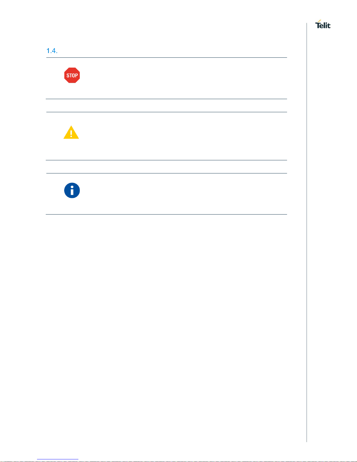
Text Conventions
Danger – This information MUST be followed or catastrophic
equipment failure or bodily injury may occur.
Caution or Warning – Alerts the user to important points about
integrating the module, if these points are not followed, the module and
end user equipment may fail or malfunction.
Tip or Information – Provides advice and suggestions that may be
useful when integrating the module.
All dates are in ISO 8601 format, i.e. YYYY-MM-DD.
Page 10

NE866B1_Hardware_Design_Guide
1VV0301354 Rev. 6 Page 10 of 70 2018-02-28
Related Documents
• SIM INTEGRATION DESIGN GUIDE 80000NT10001A
• NE866B1_NL865B1_AT_Commands_Reference_Guide 80534ST10817A
• Telit EVB User Guide 1VV0301249
• xE866_IFBD_HW_USER_GUIDE 1VV0301368
Page 11

NE866B1_Hardware_Design_Guide
1VV0301354 Rev. 6 Page 11 of 70 2018-02-28
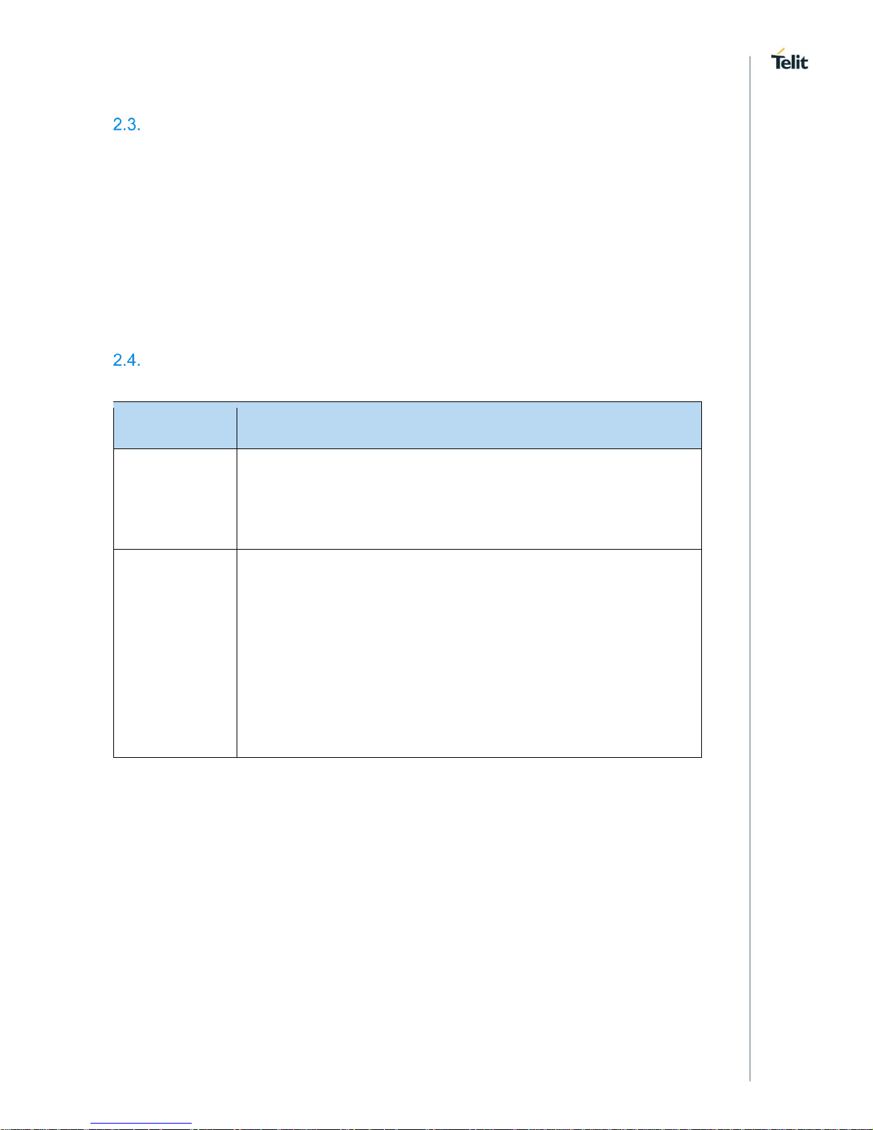
2. GENERAL PRODUCT DESCRIPTION
Overview
The NE866B1 is the first Category NB1 - aka Narrowband IoT (NB-IoT) - product in the Telit
portfolio. Specified in the Release 13 of the 3GPP standard, Cat NB1 devices are
specifically tailored for IoT applications, offering optimized power consumption and
enhanced coverage. In addition, with its ultra compact 15 x 19 mm LGA footprint, the
NE866B1 is designed for size sensitive applications.
This next generation of products supports the new features specified by 3GPP to boost IoT
applications, such as the Power Saving Mode (PSM) and the extended Discontinuous
Reception (eDRX), which allow the devices to wake up periodically to deliver only very small
amounts of data to the network and then go back to sleep for most of the time, thus allowing
longer battery operation. Enhanced coverage, with up to +20dB in maximum coupling loss
(MCL) compared to the other cellular technologies, is also one of the key benefits of this
new LTE flavor. LTE Cat NB1 devices are therefore optimized in cost, size and power
consumption compared to higher UE categories. These advantages make the NE866B1 the
perfect platform to enable a quick implementation of LTE technology in IoT/M2M where low
cost and low power are more relevant than high speed.
The NE866B1 helps increase the addressable market for LTE technology to include a broad
range of new applications and use cases best served with lower maximum data rate, ultralow power, reduced complexity and cost. Some examples are smart metering, smart
parking, smart agriculture, waste collection, industrial sensors, healthcare monitors, home
automation, and many more low data rate IoT devices. The NE866B1 is offered in a dualband configuration for deployment in the European and Chinese NB-IoT networks, either in
in-band, guard-band or standalone mode; additional regional variants will follow. It is highly
recommended for new designs, but also in particular as a migration path for existing GPRS
devices, both new and updated designs benefit from a significant extension in lifecycle with
LTE Cat NB1.
The NE866B1 supports embedded SIM chip as a mounting option, making it the ideal
solution for durable and rugged designs, and reducing BOM cost and size on the customer’s
application.
Product Variants and Frequency Bands
NE866B1 bands combinations are listed below:
Product
2G Band
(MHz)
3G Band
(MHz)
4G Band
(MHz)
Region
NE866B1-E1
B20 (800)
B8 (900)
Europe
Refer to Chapter 13 for details information about frequencies and bands.
Page 12
NE866B1_Hardware_Design_Guide
1VV0301354 Rev. 6 Page 12 of 70 2018-02-28
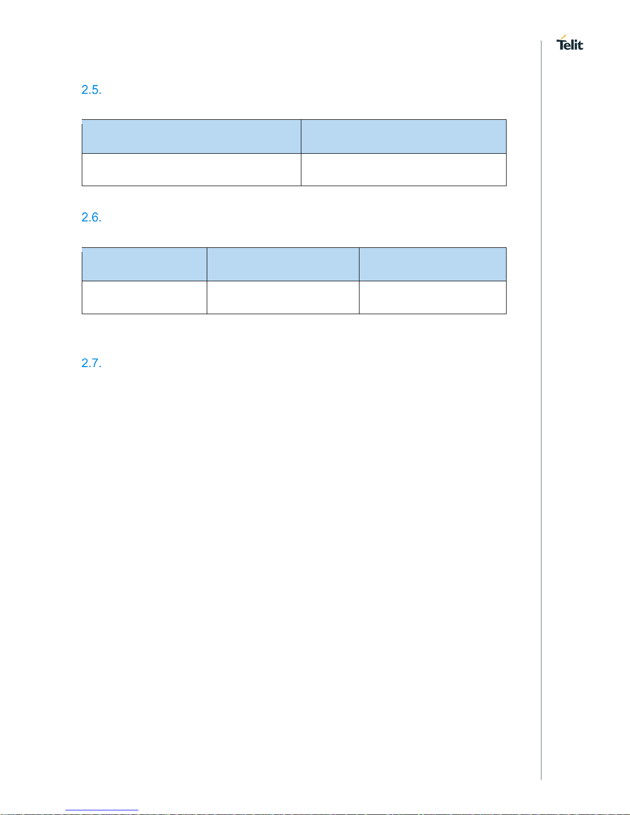
Target market
NE866B1 can be used for IoT applications, where low power consumption and enhanced
coverage are required rather than high speed data, for example:
• Smart metering
• Smart parking
• Smart agriculture
• Waste collection
• Industrial sensors
• Healthcare monitors
• Home automation
Main features
Function
Features
Modem
• NB-IoT cellular modem for low BW data communication
• Real Time Clock
• Internal IP stack
Interfaces
• Main UART for AT commands
• Auxiliary UART
• I2C
• SPI
• GPIOs
• ADC
• Antenna ports
Page 13
NE866B1_Hardware_Design_Guide
1VV0301354 Rev. 6 Page 13 of 70 2018-02-28
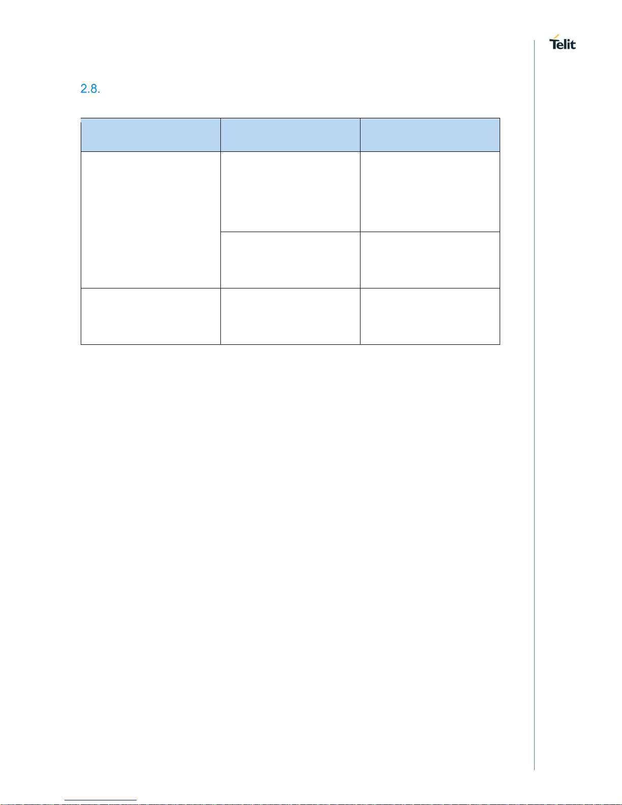
TX Output Power
Band
Power class
LTE All Bands
Class 3 (23dBm)
RX Sensitivity
Product
Band
Sensitivity (dBm)
NE866-B1-E1
B8, B20
-113
Mechanical specifications
2.7.1. Dimensions
The overall dimensions of NE866 family are:
Length: 19 mm
Width: 15 mm
Thickness: 2.2 mm
2.7.2. Weight
The nominal weight of the module is 1.5 grams.
Page 14
NE866B1_Hardware_Design_Guide
1VV0301354 Rev. 6 Page 14 of 70 2018-02-28
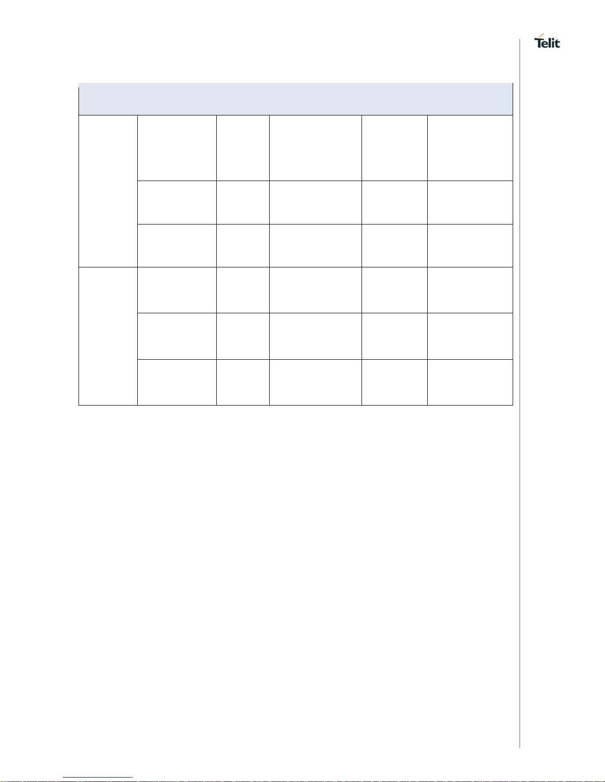
Temperature range
Case
Range
Note
Operating Temperature
Range
–20°C ÷ +55°C
The module is fully
functional(*) in all the
temperature range, and it
fully meets the 3GPP
specifications.
–40°C ÷ +85°C
The module is fully
functional (*) in all the
temperature range.
Storage and non-
operating Temperature
Range
–40°C ÷ +85°C
(*) Functional: the module is able to make and receive data calls and SMS.
Page 15

NE866B1_Hardware_Design_Guide
1VV0301354 Rev. 6 Page 15 of 70 2018-02-28
3. PINS ALLOCATION
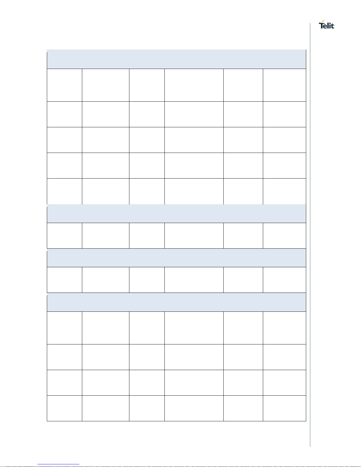
Pin-out
Pin
Signal
I/O
Function
Type
Comment
Asynchronous Serial Port - Prog. / Data / SPI / I2C / GPIO
A4
TXD
I
Serial data input
from DTE
CMOS 1.8V
A5
RXD
O
Serial data output
to DTE
CMOS 1.8V
B1
GPIO1
I/O
GPIO
CMOS 1.8V
Default
function
SPI_CS
O
SPI External CS
CMOS 1.8V
Alternate
Function
I2C_SDA
I/O
I2C Data
CMOS 1.8V
Alternate
Function
A1
SPI_CLK
O
SPI Clock
CMOS 1.8V
Page 16
NE866B1_Hardware_Design_Guide
1VV0301354 Rev. 6 Page 16 of 70 2018-02-28
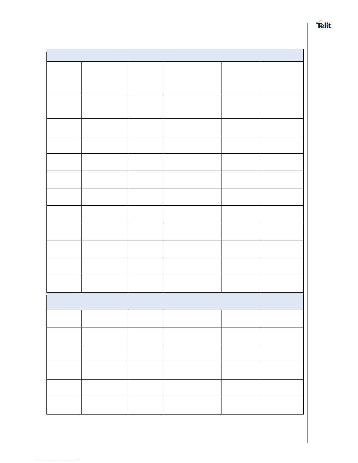
Asynchronous Auxiliary Serial Port 2 / SPI / I2C / GPIO
C1
TX_AUX
O
Auxiliary UART
(TX Data to DTE)
CMOS 1.8V
Primary Logging
Port
Default Function
SPI_MOSI
O
SPI Master Data
Out
CMOS 1.8V
Alternate
Function
GPIO2
I/O
GPIO
CMOS 1.8V
Alternate
Function
C2
GPIO3
I/O
GPIO
CMOS 1.8V
Default Function
SPI_MISO
I
SPI Master Data
In
CMOS 1.8V
Alternate
Function
I2C_SCL
I/O
I2C Clock
CMOS 1.8V
Alternate
Function
Page 17
NE866B1_Hardware_Design_Guide
1VV0301354 Rev. 6 Page 17 of 70 2018-02-28
SIM card interface
C7
SIMVCC
-
External SIM signal
– Power supply for
the SIM
1.8V Only
See next
chapters
B7
SIMRST
O
External SIM signal
– Reset
CMOS 1.8
A7
SIMCLK
O
External SIM signal
– Clock
CMOS 1.8
A6
SIMIO
I/O
External SIM– Data
I/O
CMOS 1.8
B5
SIMIN
I
SIM Presence
input
CMOS 1.8
See next
chapters
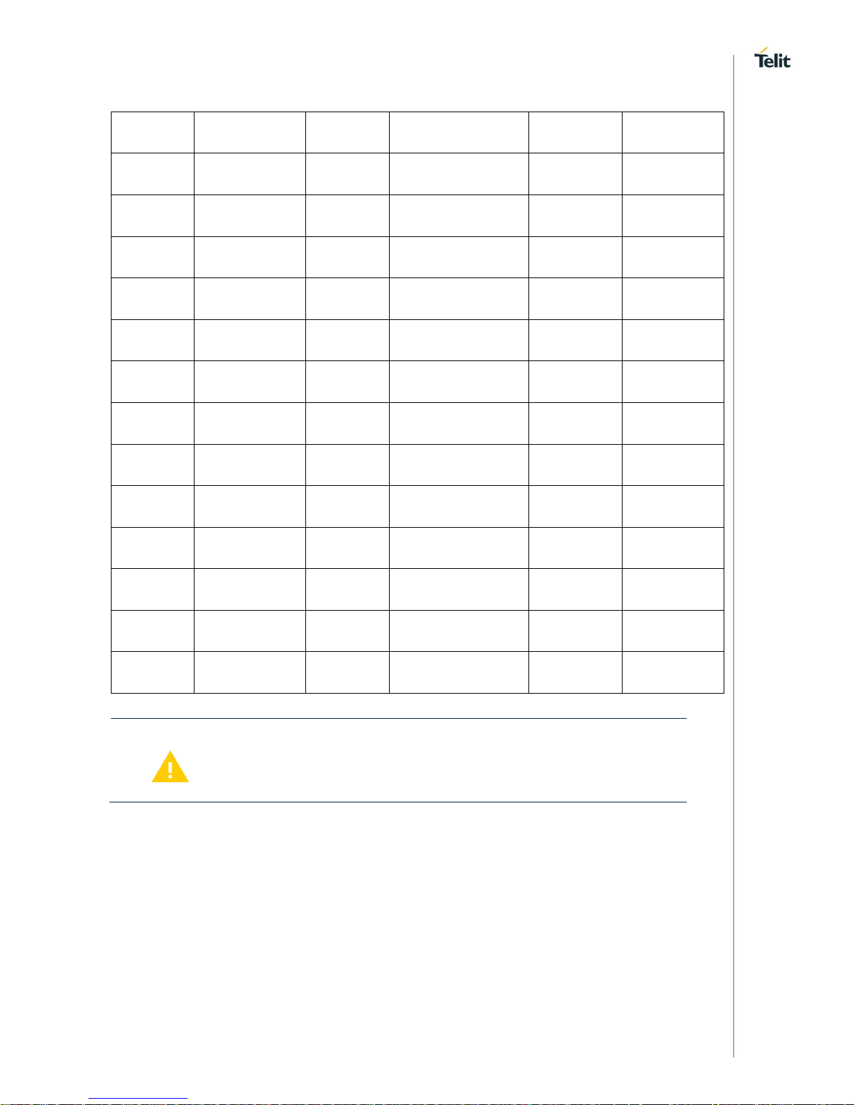
ADC
F4
ADC_IN1
AI
Analog/Digital
converter input
A/D
RF Section
G2
ANT
I/O
LTE Main Antenna
(50 ohm)
RF
Miscellaneous Functions
G4
RESET*
I
Reset Input
VBATT
Pull up to
VBATT
(10Kohm)
G5
SLP_IND
O
Modem Sleep or
PSM Indication
CMOS 1.8
Do not Drive
this pad
G6
VAUX/POWE
RMON
O
1.8V stabilized
output
Power
D3
LP_WAKE
I
LPM / PSM Wake
Up
Analog
Page 18
NE866B1_Hardware_Design_Guide
1VV0301354 Rev. 6 Page 18 of 70 2018-02-28
Power Supply
E1
VBATT
-
Main power supply
(Baseband)
Power
E2
VBATT
-
Main power supply
(Baseband)
Power
D1
GND
-
Ground
Power
F1
GND
-
Ground
Power
G1
GND
-
Ground
Power
D2
GND
-
Ground
Power
F2
GND
-
Ground
Power
C3
GND
-
Ground
Power
E3
GND
-
Ground
Power
F3
GND
-
Ground
Power
G3
GND
-
Ground
Power
F6
GND
-
Ground
Power
Reserved pins
A2
RESERVED
-
RESERVED
A3
RESERVED
-
RESERVED
B2
RESERVED
-
RESERVED
B3
RESERVED
-
RESERVED
B4
RESERVED
-
RESERVED
B6
RESERVED
-
RESERVED
Page 19
NE866B1_Hardware_Design_Guide
1VV0301354 Rev. 6 Page 19 of 70 2018-02-28
C4
RESERVED
-
RESERVED
C5
RESERVED
-
RESERVED
C6
RESERVED
-
RESERVED
D4
RESERVED
-
RESERVED
D5
RESERVED
-
RESERVED
D6
RESERVED
-
RESERVED
D7
RESERVED
-
RESERVED
E4
RESERVED
-
RESERVED
E5
RESERVED
-
RESERVED
E6
RESERVED
-
RESERVED
E7
RESERVED
-
RESERVED
F5
RESERVED
-
RESERVED
F7
RESERVED
-
RESERVED
G7
RESERVED
-
RESERVED
WARNING:
Reserved pins must not be connected
Page 20
NE866B1_Hardware_Design_Guide
1VV0301354 Rev. 6 Page 20 of 70 2018-02-28
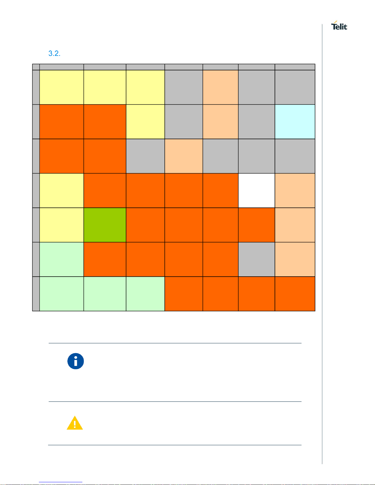
LGA Pads Layout
TOP VIEW
NOTE:
Alternate functions are marked with dark blue text while default
functions are black text
For more information, please refer to the related SW documentation
WARNING
Reserved pins must not be connected.
A B C D E F G
1 SPI_CLK
GPIO1
SPI_CS
I2C_SDA
TX AUX
SPI_MOSI
GPIO2
GND VBATT GND GND
2 RFU RFU
GPIO3
SPI_MISO
I2C_SCL
GND VBATT GND ANT
3 RFU RFU GND LP_WAKE GND GND GND
4 TXD RFU RFU RFU RFU ADC_IN1 RESET*
5 RXD SIM_IN RFU RFU RFU RFU SLP_IND
6 SIMIO RFU RFU RFU RFU GND VAUX/PWRMON
7 SIMCLK SIMRST SIMVCC RFU RFU RFU RFU
Page 21
NE866B1_Hardware_Design_Guide
1VV0301354 Rev. 6 Page 21 of 70 2018-02-28
4. POWER SUPPLY
The power supply circuitry and board layout are a very important part in the full product
design and they strongly reflect on the product overall performances, hence read carefully
the requirements and the guidelines that will follow for a proper design.
Power Supply Requirements
The external power supply must be connected to VBATT signal and must fulfil the
following requirements:
Power Supply
Value
Power Supply
Nominal Supply Voltage
3.8V
Nominal Supply Voltage
Normal Operating Voltage
Range
3.40 V÷ 4.20 V
Normal Operating Voltage
Range
Extended Operating
Voltage Range
3.10 V÷ 4.20 V
Extended Operating
Voltage Range
NOTE:
The Operating Voltage Range MUST never be exceeded; care must
be taken when designing the application’s power supply section to
avoid having an excessive voltage drop.
If the voltage drop is exceeding the limits it could cause a Power Off
of the module.
Overshoot voltage (regarding MAX Extended Operating Voltage) and
drop in voltage (regarding MIN Extended Operating Voltage) MUST
never be exceeded;
The “Extended Operating Voltage Range” can be used only with
completely assumption and application of the HW User guide
suggestions.
Page 22

NE866B1_Hardware_Design_Guide
1VV0301354 Rev. 6 Page 22 of 70 2018-02-28
Power Consumption
Mode
Typical
Mode Description
AT+CFUN=1
2 mA
Normal mode - Full functionality with PSM
disabled. (module is idle @DRX Mode with
1.28 sec paging cycle)
AT+CFUN=0
< 4 µA
TX/RX disabled, module is not registered to
the network
DRX paging modes (Full
functionality with power saving
enabled)
377.8 µA
TX=22dBm, T3324 = 30sec,
T3412 = 2621.44 s (~44min)
95.2 µA
TX=22dBm, T3324 = 30sec,
T3412 = 10485.76s (~175 min)
246.3 µA
C-eDRX = 10.24 sec
AT#PSM = 1
< 4 µA
Power Saving Enabled
NB-IoT Data Call
90mA
BW=3.75KHz, Single tone data call
(TX=0dBm)
90mA
BW=15KHz, Single tone data call
(TX=0dBm)
155 mA
BW=3.75KHz, Single tone data call
(TX=20dBm)
155 mA
BW=15KHz, Single tone data call
(TX=20dBm)
195 mA
BW=3.75KHz, Single tone data call
(TX=23dBm)
195 mA
BW=3.75KHz, Single tone data call
(TX=23dBm)
Current consumptions specification refers to typical samples and typical material.
Values represent an average measurement done over few seconds.
Values may vary depending on network and environmental conditions. Power
consumptions values obtained with VBATT = 3.8V
Page 23

NE866B1_Hardware_Design_Guide
1VV0301354 Rev. 6 Page 23 of 70 2018-02-28
General Design Rules
The principal guidelines for the Power Supply Design embrace three different design steps:
• The electrical design
• The thermal design
• The PCB layout.
4.3.1. Electrical Design Guidelines
The electrical design of the power supply depends strongly from the power source where
this power is drained. We will distinguish them into three categories:
• +5V input (typically PC internal regulator output)
• +12V input (typically automotive)
• Battery
4.3.1.1. +5V Source Power Supply Design Guidelines
• The desired output for the power supply is 3.8V, hence there's not a big difference
between the input source and the desired output and a linear regulator can be
used. A switching power supply will not be suited because of the low drop out
requirements.
• When using a linear regulator, a proper heat sink shall be provided in order to
dissipate the power generated.
• A Bypass low ESR capacitor of adequate capacity must be provided in order to cut
the current absorption peaks close to the Module, a 100μF capacitor is usually
suited.
• Make sure the low ESR capacitor on the power supply output rated at least 10V.
An example of linear regulator with 5V input is:
Page 24

NE866B1_Hardware_Design_Guide
1VV0301354 Rev. 6 Page 24 of 70 2018-02-28
4.3.1.2. +12V Source Power Supply Design Guidelines
• The desired output for the power supply is 3.8V, hence due to the big difference
between the input source and the desired output, a linear regulator is not suited and
shall not be used. A switching power supply will be preferable because of its better
efficiency.
• When using a switching regulator, a 500kHz or more switching frequency regulator
is preferable because of its smaller inductor size and its faster transient response.
This allows the regulator to respond quickly to the current peaks absorption.
• In any case the frequency and Switching design selection is related to the
application to be developed due to the fact the switching frequency could also
generate EMC interferences.
• For car PB battery the input voltage can rise up to 15,8V and this should be kept in
mind when choosing components: all components in the power supply must
withstand this voltage.
• A Bypass low ESR capacitor of adequate capacity must be provided in order to cut
the current absorption peaks, a 100μF capacitor is usually suited.
• Make sure the low ESR capacitor on the power supply output is rated at least 10V.
For Car applications, a spike protection diode should be inserted close to the
power input, in order to clean the supply from spikes.
An example of switching regulator with 12V input is in the below schematic:
Page 25

NE866B1_Hardware_Design_Guide
1VV0301354 Rev. 6 Page 25 of 70 2018-02-28
4.3.1.3. Battery Source Power Supply Design Guidelines
The desired nominal output for the power supply is 3.8V and the maximum voltage allowed
is 4.2V, hence a single 3.7V Li-Ion cell battery type is suited for supplying the power to the
Telit NB866B1 module.
• A Bypass low ESR capacitor of adequate capacity must be provided in order to cut
the current absorption peaks, a 100μF tantalum capacitor is usually suited.
• Make sure the low ESR capacitor (usually a tantalum one) is rated at least 10V.
• A protection diode should be inserted close to the power input, in order to save the
NB866B1 from power polarity inversion. Otherwise the battery connector should be
done in a way to avoid polarity inversions when connecting the battery.
• The selected battery should be capable of supporting the max peak currents of
~0.5A.
NOTE:
DON'T USE any Ni-Cd, Ni-MH, and Pb battery types directly
connected with NB866B1. Their use can lead to overvoltage on the
NB866B1 and damage it. USE ONLY Li-Ion battery types.
Page 26

NE866B1_Hardware_Design_Guide
1VV0301354 Rev. 6 Page 26 of 70 2018-02-28
4.3.2. Thermal Design Guidelines
The thermal design for the power supply heat sink should be done with the following
specifications:
• Average current consumption during NB-IoT transmission @ Max PWR level at min
battery level : 195 mA
• Average current during idle: 5.3 mA
Considering the very low current during idle, especially if Power Saving function is enabled,
it is possible to consider from the thermal point of view that the device absorbs current
significantly only during calls.
If we assume that the device stays into transmission for short periods of time (let's say few
minutes) and then remains for a quite long time in idle (let's say one hour), then the power
supply has always the time to cool down between the calls and the heat sink could be
smaller than the calculated one for 300mA maximum RMS current, or even could be the
simple chip package (no heat sink).
Moreover, in the average network conditions the device is requested to transmit at a lower
power level than the maximum and hence the current consumption will be less than the
195mA (@23dBm), being usually around 150 mA (@20dBm).
For these reasons the thermal design is rarely a concern and the simple ground plane where
the power supply chip is placed can be enough to ensure a good thermal condition and
avoid overheating.
The generated heat will be mostly conducted to the ground plane under the NE866B1; you
must ensure that your application can dissipate it.
NOTE:
The average consumption during transmissions depends on the
power level at which the device is requested to transmit by the
network. The average current consumption hence varies significantly.
Page 27

NE866B1_Hardware_Design_Guide
1VV0301354 Rev. 6 Page 27 of 70 2018-02-28
4.3.3. Power Supply PCB layout Guidelines
As seen on the electrical design guidelines the power supply shall have a low ESR capacitor
on the output to cut the current peaks on the input to protect the supply from spikes. The
placement of this component is crucial for the correct working of the circuitry. A misplaced
component can be useless or can even decrease the power supply performances.
• The Bypass low ESR capacitor must be placed close to the Telit NE866B1 power
input pads or in the case the power supply is a switching type it can be placed close
to the inductor to cut the ripple provided the PCB trace from the capacitor to the
NB866B1 is wide enough to ensure a dropless connection even during an 1A current
peak.
• The protection diode must be placed close to the input connector where the power
source is drained.
• The PCB traces from the input connector to the power regulator IC must be wide
enough to ensure no voltage drops occur when a 1A current peak is absorbed.
• The PCB traces to the NB866B1 and the Bypass capacitor must be wide enough to
ensure no significant voltage drops occur. This is for the same reason as previous
point. Try to keep this trace as short as possible.
• To reduce the EMI due to switching, it is important to keep very small the mesh
involved; thus, the input capacitor, the output diode (if not embodied in the IC) and
the regulator have to form a very small loop. This is done in order to reduce the
radiated field (noise) at the switching frequency (100-500 kHz usually).
• A dedicated ground for the Switching regulator separated by the common ground
plane is suggested.
• The placement of the power supply on the board should be done in such a way to
guarantee that the high current return paths in the ground plane are not overlapped
to any noise sensitive circuitry as the microphone amplifier/buffer or earphone
amplifier.
• The power supply input cables should be kept separate from noise sensitive lines
such as microphone/earphone cables.
• The insertion of EMI filter on VBATT pins is suggested in those designs where
antenna is placed close to battery or supply lines.
A ferrite bead like Murata BLM18EG101TN1 or Taiyo Yuden P/N
FBMH1608HM101 can be used for this purpose.
The below figure shows the recommended circuit:
Page 28

NE866B1_Hardware_Design_Guide
1VV0301354 Rev. 6 Page 28 of 70 2018-02-28
VAUX/PWRMON Power Output
A 1.8V regulated power supply output is provided in order to supply small devices from
the module. The signal is present on Pad G6
This output is always active as long as the module is powered (VBATT applied). It is also
active during module sleep mode/ PSM mode.
The operating range characteristics of the supply are:
Item
Min
Typical
Max
Output voltage
1.7V
1.80V
1.9V
Output current - -
50mA
Output bypass
capacitor
(inside the module)
100nF
NOTE:
The Output Current MUST never be exceeded; care must be taken
when designing the application section to avoid having an excessive
current consumption.
If the Current is exceeding the limits it could cause a Power Off of the
module.
Warning:
The current consumption from VAUX/PWRMON increases the
modem temperature.
Page 29

NE866B1_Hardware_Design_Guide
1VV0301354 Rev. 6 Page 29 of 70 2018-02-28
3GPP Power Saving Mode (PSM)
The NE866 is supporting a new feature introduced in 3GPP Rel.12 that allows the Module
to skip idle mode tasks for a longer time period while still maintaining the NAS context.
This feature permits to reduce the overall power consumption when there is no required
data activity with the network for a long time.
Additional hardware lines are defined to support this feature and to synchronize the
activities with the external Host processor.
PIN DESCRIPTION
Signal
Function
I/O
PAD
LP_WAKE
Low Power Wake Up.
Used to wakeup the NE866 from any of the low
power modes (either modem or apps).
I
D3
SLP_IND
Modem Sleep or PSM indication.
“0” – NE866B1 modem is in Sleep mode / PSM
“1” - NE866B1 modem is not in sleep mode /
PSM
O
G5
NOTE:
SLP_IND signal indicates the status of the modem subsystem only
SLP_IND cannot be used to determine if the entire module is at low
power mode.
Page 30

NE866B1_Hardware_Design_Guide
1VV0301354 Rev. 6 Page 30 of 70 2018-02-28
4.5.1. LP_WAKE design guide
LP Wake signal could be used by the host to wake up the NE866B1 from any of the sleep
modes (either modem sleep or application sleep or both)
LP Wake signal can be configured to wakeup the system at either rising or falling edge or
both edges.
In most cased the most convenient configuration is falling edge as shown in the application
circuit below.
NOTE:
LP_WAKE is an analog input to a comperator but should be treated
as a digital input from the application side.
• Rising edge is considured when the signal crossed the level
of 1.2V and going up.
• Faling edge is considered when the signal crossed the level of
0.7V and going down.
GND
R1
R2
Q1
From Host
Assert high for Wake
LP_WAKE
1M ohm
1.8V
Page 31

NE866B1_Hardware_Design_Guide
1VV0301354 Rev. 6 Page 31 of 70 2018-02-28
5. DIGITAL SECTION
Logic Levels
ABSOLUTE MAXIMUM RATINGS:
OPERATING RANGE - INTERFACE LEVELS (1.8V CMOS):
Parameter
Min
Max
Input high level
1.25V
1.95V
Input low level
0V
0.35V
Output high level
1.42V
1.85V
Output low level
0V
0.2V
LEAKAGE CURRENT CHARACTERISTICS:
Parameter
AVG
Input leakage current
±10uA
Output leakage current
±10uA
DRIVE STRENGTH
Parameter
AVG
Max drive strength
10mA
Parameter
Min
Max
Input level on any digital pin (CMOS 1.8) with respect
to ground
-0.3V
2.1V
Input level on any digital pin (CMOS 1.8) with respect
to ground
when VBATT is not supplied
-0.3V
0.3V
Page 32

NE866B1_Hardware_Design_Guide
1VV0301354 Rev. 6 Page 32 of 70 2018-02-28
Power On
The NB866B1 will automatically power on itself when VBATT is applied to the module.
VAUX / PWRMON pin will be then set at the high logic level.
The following flow chart shows the proper turn on procedure:
PWRMON=ON
?
“Modem ON Proc”
START
PWR Supply ON
PWRMON=ON
?
Delay = 8 s
AT Init Sequence
Enter AT<CR>
Delay 1s – 5s
Delay = 8 sec
Start AT CMD
AT Answer in
1sec?
Modem Reset Proc
Page 33

NE866B1_Hardware_Design_Guide
1VV0301354 Rev. 6 Page 33 of 70 2018-02-28
A flow chart showing the AT commands managing procedure is displayed below:
“Start AT CMD”
START
Delay = 300 msec
Enter AT <CR>
Disconnect PWR Supply
AT answer in
1 sec ?
GO TO
“Modem ON Proc.”
“Start AT CMD”
END
Page 34

NE866B1_Hardware_Design_Guide
1VV0301354 Rev. 6 Page 34 of 70 2018-02-28
Unconditional Restart
To unconditionally restart the NE866B1, the pad RESET* must be tied low for at least 200
milliseconds and then released.
The maximum current that can be drained from the RESET* pad is 1 mA.
The hardware unconditional Restart must not be used during normal operation of the
device since it does not detach the device from the network. It shall be kept as an
emergency exit procedure to be done in the rare case that the device gets stuck waiting
for some network or SIM responses.
Do not use any pull up resistor on the RESET* line nor any totem pole digital output.
Using pull up resistor may bring to latch up problems on the NE866B1 power regulator
and improper functioning of the module.
The line RESET* must be connected only in open collector configuration; the transistor
must be connected as close as possible to the RESET* pin.
The unconditional hardware restart must always be implemented on the application board
as the software must be able to use it as an emergency exit procedure.
PIN DESCRIPTION
Signal
Function
I/O
PAD
RESET*
Unconditional Reset of the Module
I
G4
OPERATING LEVELS
The RESET* line is connected to 1.8V with a Pull Up so the electrical levels are on this pin
are aligned with the other CMOS 1.8V digital I/O’s.
WARNING:
The hardware unconditional Reset must not be used during normal
operation of the device since it does not detach the device from the
network. It shall be kept as an emergency exit procedure.
Page 35

NE866B1_Hardware_Design_Guide
1VV0301354 Rev. 6 Page 35 of 70 2018-02-28
A typical circuit for implementing an unconditional RESET is shown below:
NOTE:
In order to avoid a back powering effect it is recommended to avoid
having any HIGH logic level signal applied to the digital pins of the
NE866B1 when the module is powered off or during a reboot
transition.
Using bidirectional level translators which do not support High Z
mode during power off is not recommended.
Page 36

NE866B1_Hardware_Design_Guide
1VV0301354 Rev. 6 Page 36 of 70 2018-02-28
In the following flow chart is detailed the proper restart procedure:
In order to prevent a back powering effect it is recommended to avoid
having any HIGH logic level signal applied to the digital pins of the
NE866B1 when the module is powered OFF or during an ON/OFF
transition.
Using bidirectional level translators which do not support High Z
mode during power off is not recommended.
Modem Reset
Proc.
Reset = LOW
Delay 200ms
Delay 1s
Apply Power
On Procedure
Page 37

NE866B1_Hardware_Design_Guide
1VV0301354 Rev. 6 Page 37 of 70 2018-02-28
Power OFF procedure
The NE866B1 does not provide any means of software driven shutdown.
In case that power off is required (for example when modem is not used for a long time),
the below procedure should be followed in order to eliminate any possible damage due to
unexpected power cut.
WARNING:
Please carefully follow the recommended procedure for shut down and
power off.
Not following the recommended shut-down and power off procedures might
damage the device and consequently void the warranty.
Modem Power Off
Proc
AT+CFUN=0
In PSM mode?
AT+COPS=2
Yes
No
Power Off supply
Page 38

NE866B1_Hardware_Design_Guide
1VV0301354 Rev. 6 Page 38 of 70 2018-02-28
Communication ports
5.5.1. Serial Ports
The NB866B1 module is provided with by 2 Asynchronous serial ports:
• MODEM SERIAL PORT 1 (Main)
• MODEM SERIAL PORT 2 (TX Only, used for logging)
Several configurations can be designed for the serial port on the OEM hardware, but the
most common are:
• RS232 PC com port
• microcontroller UART @ 1.8V (Universal Asynchronous Receive Transmit)
• microcontroller UART @ 5V or other voltages different from 1.8V
Depending from the type of serial port on the OEM hardware a level translator circuit may
be needed to make the system work.
On the NB866B1 the ports are CMOS 1.8.
5.5.1.1. MODEM SERIAL PORT 1
The serial port 1 on the NB866B1 is a +1.8V UART with only 2 RS232 signals.
It differs from the PC-RS232 in the signal polarity (RS232 is reversed) and levels.
Serial port 1 is considered a “low power UART” and is avalable during LPM and PSM
such that any activity in the TXD pin (NE866B1 input) will wakeup the system.
The following table lists the signals of Serial port 1:
RS232
Pin
Signal
Pad
Name
Usage
2
RXD
A5
Transmit line *see
Note
Output transmit line of NB866B1
UART
3
TXD
A4
Receive line *see
Note
Input receive of the NB866B1
UART
This pin also serves as a sleep
wakeup source.
5
GND
D1, F1, G1,
D2, F2, C3,
E3, F3, G3, F6
Ground
Ground
Page 39

NE866B1_Hardware_Design_Guide
1VV0301354 Rev. 6 Page 39 of 70 2018-02-28
NOTE:
According to V.24, some signal names are referred to the application
side, therefore on the NB866B1 side these signal are on the opposite
direction:
TXD on the application side will be connected to the receive line
(here named TXD)
RXD on the application side will be connected to the transmit line
(here named RXD)
For a minimum implementation, only the TXD, RXD lines can be
connected.
In order to avoid a back powering effect it is recommended to avoid
having any HIGH logic level signal applied to the digital pins of the
NB866B1 when the module is powered off or during a reboot
transition.
Using bidirectional level translators which do not support High Z
mode during power off is not recommended.
NOTE:
By default, since UART port uses the low power mode, HW flow
control is not used
Page 40

NE866B1_Hardware_Design_Guide
1VV0301354 Rev. 6 Page 40 of 70 2018-02-28
5.5.1.2. MODEM SERIAL PORT 2
The secondary serial port on the NB866B1 is a CMOS1.8V with only TX signal which is
used for logging.
The signals of the NB866B1 serial port are:
PAD
Signal
I/O
Function
Type
NOTE
C1
TX_AUX
O
Auxiliary UART (TX Data
to DTE)
CMOS
1.8V
Main Debug & logging
port
NOTE:
In order to avoid a back powering effect it is recommended to avoid
having any HIGH logic level signal applied to the digital pins of the
NB866B1 when the module is not supplied or during a
powerup/reboot transition.
Using bidirectional level translators which do not support High Z
mode during power off is not recommended.
NOTE:
TX_AUX is shared with SPI functionality
SPI and AUX UART cannot work simultaniously
5.5.1.3. RS232 LEVEL TRANSLATION
In order to interface the NB866B1 with a PC com port or a RS232 (EIA/TIA-232) application
a level translator is required. This level translator must:
• invert the electrical signal in both directions;
• Change the level from 0/1.8V to +15/-15V.
The RS232 UART 16450, 16550, 16650 & 16750 chipsets accept signals with lower levels
on the RS232 side (EIA/TIA-562), allowing a lower voltage-multiplying ratio on the level
translator. Note that the negative signal voltage must be less than 0V and hence some sort
of level translation is always required.
The simplest way to translate the levels and invert the signal is by using a single chip level
translator. There are a multitude of them, differing in the number of drivers and receivers
and in the levels (be sure to get a true RS232 level translator not a RS485 or other
standards).
Page 41

NE866B1_Hardware_Design_Guide
1VV0301354 Rev. 6 Page 41 of 70 2018-02-28
By convention the driver is the level translator from the 0-1.8V UART to the RS232 level.
The receiver is the translator from the RS232 level to 0-1.8V UART.
In order to translate the whole set of control lines of the UART you will need:
• 5 drivers
• 3 receivers
An example of RS232 level adaptation circuitry could be done using a MAXIM transceiver
(MAX218).
In this case the chipset is capable to translate directly from 1.8V to the RS232 levels
(Example done on 4 signals only).
NOTE:
The digital input lines operating at 1.8V CMOS have an absolute
maximum input voltage of 2.2V. The level translator IC outputs on the
module side (i.e. module inputs) will cause damage to the module
inputs if the level translator is powered by a +3.8V supply. So the
level translator IC must be powered from a dedicated +1.8V power
supply to match the module I/O level.
The RS232 serial port lines are usually connected to a DB9 connector with the following
layout:
Page 42

NE866B1_Hardware_Design_Guide
1VV0301354 Rev. 6 Page 42 of 70 2018-02-28
General purpose I/O
The NB866B1 module is provided by a set of Configurable Digital Input / Output pins
(CMOS 1.8V)
Input pads can only be read; they report the digital value (high or low) present on the pad
at the read time.
Output pads can only be written or queried and set the value of the pad output.
Alternate functionality is avalable for the GPIO's as shown in the below table.
The alternate functinality is selected as a group and by function rather than by pad.
Please refer to the AT Commands User Guide for more details on selecting the pads
alternate functinality.
The following table shows the available GPIO's on the NB866B1 and their functionality:
PAD
Signal
Default
Function
Alt Func #1
(I2C + GPIO)
Alt Func #2
(I2C + Log)
Alt Func #3
(GPIO)
Alt Func #4
(SPI)
B1
GPIO1
GPIO1
I2C_SDA
I2C_SDA
GPIO1
SPI_CS
C1
GPIO2
TX_AUX
GPIO2
TX_AUX
GPIO2
SPI_MOSI
C2
GPIO3
GPIO3
I2C_CLK
I2C_CLK
GPIO3
SPI_MISO
NOTE:
When using SPI functionality, the SPI_CLK function is assigned to
pad A1.
NOTE:
The internal GPIO’s pull up/pull down could be set to the preferred
status for the application using the AT#GPIO command.
Please refer for the AT Commands User Guide for the detailed
command Syntax.
WARNING:
During power up the GPIOs may be subject to transient glitches.
Page 43

NE866B1_Hardware_Design_Guide
1VV0301354 Rev. 6 Page 43 of 70 2018-02-28
5.6.1. Using a GPIO as an INPUT
The GPIO pads, when used as inputs, can be connected to a digital output of another
device and report its status, provided this device has interface levels compatible with the
1.8V CMOS levels of the GPIO. If the digital output of the device to be connected with the
GPIO input pad has interface levels different from the 1.8V CMOS, then it can be buffered
with an open collector transistor with a 47K pull up to VAUX.
NOTE:
In order to avoid a back powering effect it is recommended to avoid
having any HIGH logic level signal applied to the digital pins of the
NB866B1 when the module is powered off or during a
powerup/reboot transition.
Using bidirectional level translators which do not support High Z
mode during power off is not recommended.
The VAUX /PWRMON pin can be used for input pull up reference.
5.6.2. Using a GPIO as an OUTPUT
The GPIO pads, when used as outputs, can drive 1.8V CMOS digital devices or
compatible hardware. When set as outputs, the pads have a push-pull output and
therefore the pull-up resistor may be omitted.
Page 44

NE866B1_Hardware_Design_Guide
1VV0301354 Rev. 6 Page 44 of 70 2018-02-28
I2C Port
The NE866B1 supports a dedicated port for I2C communication
I2C speed is limited to 10KHz.
The following table lists the available I2C signals on the NE866B1:
PAD
Signal
I/O
Default State
NOTE
B1
I2C_SDA
I/O
Pull Up
C2
I2C_SCL
I/O
Pull Up
Please refer to the AT command user guide for more information.
NOTE:
The I2C port is shared with SPI. When SPI is used, I2C cannot be
used and vice versa.
SIM Interface
The NE866B1 supports a standard SIM card interface with the below exceptions:
• 1.8V I/O only (3V SIM is not supported).
• SIM PIN (SIM lock) feature is not supported.
• SIM power OFF during PSM is an expected behavior
For more info on SIM implementation, please refer to the related User Guide (SIM Holder
Design Guides, 80000NT10001a).
5.8.1. SIMIN Detection
PIN B5 is used as SIM DETECT input.
As long as SIMIN is not pulled low by the application board the module will use the
internal eSIM.
For using an external SIM the user must assert SIMIN low
NE866B1 modules ordered without eSIM support will always use the external SIM
regardless of the SIMIN state
ADC Converter
The NB866B1 is provided by one ADC converter. It is able to read a voltage level in the
range of 0.2÷1.7 volts applied on the ADC pin input, store and convert it into 10 bit word.
The input line is named as ADC_IN1 and it is available on Pad F4
The following table is showing the ADC characteristics:
Item
Min
Typical
Max
Unit
Input Voltage range
0.2
-
1.7
Volt
AD conversion
- - 10
bits
Page 45

NE866B1_Hardware_Design_Guide
1VV0301354 Rev. 6 Page 45 of 70 2018-02-28
6. RF SECTION
Bands Variants
The following table is listing the supported Bands:
TX Output power
Product
Bands
Power Class
NE866B1-E1
FDD B8, B20
Class 3 (23dBm)
RX Sensitivity
Technology
3GPP Compliance
NB-IoT
-108.2dBm
NOTE:
For low data rates sensitivity will be better than 3GPP spec
RED requirements
• NE866B1 meets RED requirement Article 10 item 8.
• NE866B1 has been assessed to be used with separation distance more than 20cm.
• NE866B1 reference antenna: LTE MAGNETIC ANTENNA Type n° T- AT305
o 700 - 960MHz / 1710 – 2700MHz
o Antenna Gain - 2.14dBi
• The maximum antenna gain for each frequency band is:
o FDD8: 7dBi
o FDD20: 6.7dBi
Product
Supported LTE bands
NE866B1E1
FDD B8, B20
Page 46

NE866B1_Hardware_Design_Guide
1VV0301354 Rev. 6 Page 46 of 70 2018-02-28
Antenna requirements
6.5.1. Main Antenna
The antenna connection and board layout design are the most important aspect in the full
product design as they strongly affect the product overall performances, hence read
carefully and follow the requirements and the guidelines for a proper design.
The antenna and antenna transmission line on PCB for a Telit NB866B1 device shall fulfil
the following requirements:
Item
Value
Frequency range
Depending by frequency band(s) provided by the network
operator, the customer shall use the most suitable
antenna for that/those band(s)
Bandwidth
LTE Band VIII (900) : 80 MHz
LTE Band XX (800) : 71 MHz : 47 MHz
Impedance
50 ohm
Input power
> 23dBm Average power
VSWR absolute max
≤ 10:1 (limit to avoid permanent damage)
VSWR recommended
≤ 2:1 (limit to fulfill all regulatory requirements)
Page 47

NE866B1_Hardware_Design_Guide
1VV0301354 Rev. 6 Page 47 of 70 2018-02-28
6.5.2. PCB design guidelines
When using the NB866B1, since there's no antenna connector on the module, the
antenna must be connected to the NB866B1 antenna pad by means of a transmission line
implemented on the PCB.
This transmission line shall fulfil the following requirements:
The transmission line should be designed according to the following guidelines:
• Ensure that the antenna line impedance is 50 ohm;
• Keep the antenna line on the PCB as short as possible, since the antenna line loss
shall be less than 0.3 dB;
• Antenna line must have uniform characteristics, constant cross section; avoid
meanders and abrupt curves;
• Keep, if possible, one layer of the PCB used only for the Ground plane;
• Surround (on the sides, over and under) the antenna line on PCB with Ground, avoid
having other signal tracks facing directly the antenna line track;
• The ground around the antenna line on PCB has to be strictly connected to the
Ground Plane by placing vias every 2mm at least;
• Place EM noisy devices as far as possible from NB866B1 antenna line;
• Keep the antenna line far away from the NB866B1 power supply lines;
• If you have EM noisy devices around the PCB hosting the NB866B1, such as fast
switching ICs, take care of the shielding of the antenna line by burying it inside the
layers of PCB and surround it with Ground planes, or shield it with a metal frame
cover.
Item
Value
Characteristic
Impedance
50 ohm
Max Attenuation
0.3 dB
Coupling
Coupling with other signals shall be avoided
Ground Plane
Cold End (Ground Plane) of antenna shall be
equipotential to the NB866B1 ground pins
Page 48

NE866B1_Hardware_Design_Guide
1VV0301354 Rev. 6 Page 48 of 70 2018-02-28
• If you don't have EM noisy devices around the PCB of NB866B1, by using a micro
strip on the superficial copper layer for the antenna line, the line attenuation will be
lower than a buried one;
The following image is showing the
suggested layout for the
Antenna pad connection
(dimensions in mm):
NOTE:
In early samples of NE866B1 the
antenna pad has a closed ring around it
as shown below
In that case, the RF pin (G2) should be
routed through an internal layer of the
board connecting to the PAD on the top
layer ideally through a BLIND via. VIA
diameter should be chosen to achieve
best coaxiality effect thorugh the board.
It is also recommended to bring directly
to the reference RF ground layer the
GND signal present on PADs F1,
F2,F3, G1 and G3.
6.5.3. Antenna installation Guidelines
Install the antenna in a place covered by the LTE signal.
Antenna shall not be installed inside metal cases.
Antenna shall be installed also according to antenna manufacturer instructions.
Page 49

NE866B1_Hardware_Design_Guide
1VV0301354 Rev. 6 Page 49 of 70 2018-02-28
7. MECHANICAL DESIGN
Mechanical Dimensions
The NE866B1 overall dimensions are:
• Length: 19 mm
• Width: 15 mm
• Thickness: 2.2 mm
• Weight: 1.5 gr
7.1.1. Mechanical Drawing
7.1.2. Top View
The figure below shows mechanical top view of the NE866B1
Page 50

NE866B1_Hardware_Design_Guide
1VV0301354 Rev. 6 Page 50 of 70 2018-02-28
Dimensions are in mm
7.1.3. Bottom View (as seen from bottom side)
Page 51

NE866B1_Hardware_Design_Guide
1VV0301354 Rev. 6 Page 51 of 70 2018-02-28
7.1.4. Side View
Page 52

NE866B1_Hardware_Design_Guide
1VV0301354 Rev. 6 Page 52 of 70 2018-02-28
8. APPLICATION PCB DESIGN
The NB866B1 modules have been designed in order to be compliant with a standard leadfree SMT process
Recommended footprint for the application
Page 53

NE866B1_Hardware_Design_Guide
1VV0301354 Rev. 6 Page 53 of 70 2018-02-28
In order to easily rework the NB866B1 is suggested to consider on the application a 1.5
mm placement inhibit area around the module. It is also suggested, as common rule for
an SMT component, to avoid having a mechanical part of the application in direct contact
with the module.
The area under WIRING INHIBIT (see figure above) must be clear from signal or ground
paths.
PCB pad design
Non solder mask defined (NSMD) type is recommended for the solder pads on the PCB.
PCB
Copper
Pad
Solder Mask
SMD
(Solder Mask Defined)
NSMD
(Non Solder Mask Defined)
Page 54

NE866B1_Hardware_Design_Guide
1VV0301354 Rev. 6 Page 54 of 70 2018-02-28
PCB pad dimensions
The recommendation for the PCB pads dimensions are described in the following image
(dimensions in mm)
It is not recommended to place via or micro-via not covered by solder resist in an area of
0,3 mm around the pads unless it carries the same signal of the pad itself
Holes in pad are allowed only for blind holes and not for through holes.
Page 55

NE866B1_Hardware_Design_Guide
1VV0301354 Rev. 6 Page 55 of 70 2018-02-28
Recommendations for PCB pad surfaces:
Finish
Layer Thickness (um)
Properties
Electro-less Ni / Immersion
Au
3 –7 / 0.05 – 0.15
good solder ability
protection,
high shear force values
The PCB must be able to resist the higher temperatures which are occurring at the leadfree process. This issue should be discussed with the PCB-supplier. Generally, the
wettability of tin-lead solder paste on the described surface plating is better compared to
lead-free solder paste.
It is not necessary to panel the application’s PCB, however in that case it is suggested to
use milled contours and predrilled board breakouts; scoring or v-cut solutions are not
recommended.
Stencil
Minimum stencil thickness recommended is 125um (5 mil)
Solder paste
We recommend using only “no clean” solder paste in order to avoid the cleaning of
the modules after assembly.
Page 56

NE866B1_Hardware_Design_Guide
1VV0301354 Rev. 6 Page 56 of 70 2018-02-28
NE866B1 Solder reflow
Recommended solder reflow profile
Profile Feature
Pb-Free Assembly
Average ramp-up rate (TL to TP)
3°C/second max
Preheat
– Temperature Min (Tsmin)
– Temperature Max (Tsmax)
– Time (min to max) (ts)
150°C
200°C
60-180 seconds
Tsmax to TL
– Ramp-up rate
3°C/second max
Time maintained above:
– Temperature (TL)
– Time (tL)
217°C
60-150 seconds
Peak temperature (Tp)
245 +0/-5°C
Time within 5°C of actual peak temperature (tp)
10-30 seconds
Ramp-down rate
6°C/second max.
Time 25°C to peak temperature
8 minutes max.
Page 57

NE866B1_Hardware_Design_Guide
1VV0301354 Rev. 6 Page 57 of 70 2018-02-28
9. PACKING SYSTEM
Tray
The NB866B1 modules are packaged on trays
The tray is JEDEC compliant, injection molded antistatic Modified Polyphenylene ether
(MPPO). It has good thermal characteristics and can withstand a standard baking
temperature of up to 125°C, thereby avoiding handling the modules if baking is required.
The trays are rigid, thus providing mechanical protection against transport stress. In
addition, they are re-usable and so environmentally sustainable.
There are 2 (two) antistatic rubber bands that enclose each envelope.
The carton box is rigid, offering mechanical protection. The carton box has one flap across
the entire top surface. It is sealed with tape along the edges of the box.
Table 1: Tray Packing
Modules per
Tray
Trays per
Envelope
Modules per
Envelope
Envelopes per Carton
Box
Modules per
Box
98
4+ 1 empty
392
5
1960
Table 2: Packing Quantities
Order Type
Quantity
Minimum Order Quantity (MOQ)
98
Standard Packing Quantity (SPQ)
392
Page 58

NE866B1_Hardware_Design_Guide
1VV0301354 Rev. 6 Page 58 of 70 2018-02-28
Tray organization is shown in the figure below
Page 59

NE866B1_Hardware_Design_Guide
1VV0301354 Rev. 6 Page 59 of 70 2018-02-28
Tray Drawing
WARNING:
These trays can withstand a maximum temperature of 125℃.
Page 60

NE866B1_Hardware_Design_Guide
1VV0301354 Rev. 6 Page 60 of 70 2018-02-28
Tape & Reel
The NE866 modules are available on a T&R packaging as well
NE866B1 is packaged on reels of 200 pieces each as shown in the figure below.
Page 61

NE866B1_Hardware_Design_Guide
1VV0301354 Rev. 6 Page 61 of 70 2018-02-28
Carrier Tape Drawing
Moisture sensitivity
The NB866B1 is a Moisture Sensitive Device level 3, in according with standard
IPC/JEDEC J-STD-020, take care all the relatives requirements for using this kind of
components.
Moreover, the customer has to take care of the following conditions:
a) Calculated shelf life in sealed bag: 12 months at <40°C and <90% relative humidity
(RH).
b) Environmental condition during the production: 30°C / 60% RH according to
IPC/JEDEC J-STD-033A paragraph 5.
c) The maximum time between the opening of the sealed bag and the reflow process must
be 168 hours if condition b) “IPC/JEDEC J-STD-033A paragraph 5.2” is respected
d) Baking is required if conditions b) or c) are not respected
e) Baking is required if the humidity indicator inside the bag indicates 10% RH or more
Page 62

NE866B1_Hardware_Design_Guide
1VV0301354 Rev. 6 Page 62 of 70 2018-02-28
10. CONFORMITY ASSESSMENT ISSUES
Declaration of Conformity
Hereby, Telit Communications S.p.A declares that the NB IOT Module is in compliance
with Directive 2014/53/EU.
The full text of the EU declaration of conformity is available at the following internet
address: http://www.telit.com\red
Page 63

NE866B1_Hardware_Design_Guide
1VV0301354 Rev. 6 Page 63 of 70 2018-02-28
11. SAFETY RECOMMENDATIONS
READ CAREFULLY
Be sure the use of this product is allowed in the country and in the environment required.
The use of this product may be dangerous and has to be avoided in the following areas:
• Where it can interfere with other electronic devices in environments such as
hospitals, airports, aircrafts, etc.
• Where there is risk of explosion such as gasoline stations, oil refineries, etc. It is the
responsibility of the user to enforce the country regulation and the specific
environment regulation.
Do not disassemble the product; any mark of tampering will compromise the warranty
validity. We recommend following the instructions of the hardware user guides for correct
wiring of the product. The product has to be supplied with a stabilized voltage source and
the wiring has to be conformed to the security and fire prevention regulations. The product
has to be handled with care, avoiding any contact with the pins because electrostatic
discharges may damage the product itself. Same cautions have to be taken for the SIM,
checking carefully the instruction for its use. Do not insert or remove the SIM when the
product is in power saving mode.
The system integrator is responsible for the functioning of the final product; therefore, care
has to be taken to the external components of the module, as well as any project or
installation issue, because the risk of disturbing the GSM network or external devices or
having impact on the security. Should there be any doubt, please refer to the technical
documentation and the regulations in force. Every module has to be equipped with a proper
antenna with specific characteristics. The antenna has to be installed with care in order to
avoid any interference with other electronic devices and has to guarantee a minimum
distance from the body (20 cm). In case this requirement cannot be satisfied, the system
integrator has to assess the final product against the SAR regulation.
The European Community provides some Directives for the electronic equipment
introduced on the market. All of the relevant information is available on the European
Community website:
http://ec.europa.eu/enterprise/sectors/rtte/documents/
The text of the Directive 99/05 regarding telecommunication equipment is available,
while the applicable Directives (Low Voltage and EMC) are available at:
http://ec.europa.eu/enterprise/sectors/electrical/
Page 64

NE866B1_Hardware_Design_Guide
1VV0301354 Rev. 6 Page 64 of 70 2018-02-28
12. REFERENCE TABLE OF RF BANDS CHARACTERISTICS
Mode
Freq. Tx
(MHz)
Freq. Rx
(MHz)
Channels
Tx-Rx Offset
PCS 1900
1850.2 ~ 1909.8
1930.2 ~ 1989.8
512 ~ 810
80 MHz
DCS 1800
1710 ~ 1785
1805 ~ 1880
512 ~ 885
95 MHz
GSM 850
824.2 ~ 848.8
869.2 ~ 893.8
128 ~ 251
45 MHz
EGSM 900
890 ~ 915
935 ~ 960
0 ~ 124
45 MHz
880 ~ 890
925 ~ 935
975 ~ 1023
45 MHz
WCDMA 2100 – B1
1920 ~ 1980
2110 ~ 2170
Tx: 9612 ~ 9888
Rx: 10562 ~ 10838
190 MHz
WCDMA 1900 – B2
1850 ~ 1910
1930 ~ 1990
Tx: 9262 ~ 9538
Rx: 9662 ~ 9938
80 MHz
WCDMA 1800 – B3
1710 ~ 1785
1805 ~ 1880
Tx: 937 ~ 1288
Rx: 1162 ~ 1513
95 MHz
WCDMA AWS – B4
1710 ~ 1755
2110 ~ 2155
Tx: 1312 ~ 1513
Rx: 1537 ~ 1738
400 MHz
WCDMA 850 – B5
824 ~ 849
869 ~ 894
Tx: 4132 ~ 4233
Rx: 4357 ~ 4458
45 MHz
WCDMA 900 – B8
880 ~ 915
925 ~ 960
Tx: 2712 ~ 2863
Rx: 2937 ~ 3088
45 MHz
WCDMA 1800 – B9
1750 ~ 1784.8
1845 ~ 1879.8
Tx: 8762 ~ 8912
Rx: 9237 ~ 9387
95 MHz
WCDMA 800 – B19
830 ~ 845
875 ~ 890
Tx: 312 ~ 363
Rx: 712 ~ 763
45 MHz
TDSCDMA 2000 – B34
2010 ~ 2025
2010 ~ 2025
Tx: 10054 ~ 10121
Rx: 10054 ~ 10121
0 MHz
TDSCDMA 1900 – B39
1880 ~ 1920
1880 ~ 1920
Tx: 9404 ~ 9596
Rx: 9404 ~ 9596
0 MHz
LTE 2100 – B1
1920 ~ 1980
2110 ~ 2170
Tx: 18000 ~ 18599
Rx: 0 ~ 599
190 MHz
Page 65

NE866B1_Hardware_Design_Guide
1VV0301354 Rev. 6 Page 65 of 70 2018-02-28
Mode
Freq. Tx
(MHz)
Freq. Rx
(MHz)
Channels
Tx-Rx Offset
LTE 1900 – B2
1850 ~ 1910
1930 ~ 1990
Tx: 18600 ~ 19199
Rx: 600 ~ 1199
80 MHz
LTE 1800 – B3
1710 ~ 1785
1805 ~ 1880
Tx: 19200 ~ 19949
Rx: 1200 ~ 1949
95 MHz
LTE AWS – B4
1710 ~ 1755
2110 ~ 2155
Tx: 19950 ~ 20399
Rx: 1950 ~ 2399
400 MHz
LTE 850 – B5
824 ~ 849
869 ~ 894
Tx: 20400 ~ 20649
Rx: 2400 ~ 2649
45 MHz
LTE 2600 – B7
2500 ~ 2570
2620 ~ 2690
Tx: 20750 ~ 21449
Rx: 2750 ~ 3449
120 MHz
LTE 900 – B8
880 ~ 915
925 ~ 960
Tx: 21450 ~ 21799
Rx: 3450 ~ 3799
45 MHz
LTE 1800 – B9
1749.9 ~ 1784.9
1844.9 ~ 1879.9
Tx: 21800 ~ 2149
Rx: 3800 ~ 4149
95 MHz
LTE AWS+ – B10
1710 ~ 1770
2110 ~ 2170
Tx: 22150 ~ 22749
Rx: 4150 ~ 4749
400 MHz
LTE 700a – B12
699 ~ 716
729 ~ 746
Tx : 23010 ~ 23179
Rx : 5010 ~ 5179
30 MHz
LTE 700c – B13
777 ~ 787
746 ~ 756
Tx : 27210 ~ 27659
Rx : 9210 ~ 9659
-31 MHz
LTE 700b – B17
704 ~ 716
734 ~ 746
Tx: 23730 ~ 23849
Rx: 5730 ~ 5849
30 MHz
LTE 800 – B19
830 ~ 845
875 ~ 890
Tx: 24000 ~ 24149
Rx: 6000 ~ 6149
45 MHz
LTE 800 – B20
832 ~ 862
791 ~ 821
Tx: 24150 ~ 24449
Rx: 6150 ~ 6449
-41 MHz
LTE 1500 – B21
1447.9 ~ 1462.9
1495.9 ~ 1510.9
Tx: 24450 ~ 24599
Rx: 6450 ~ 6599
48 MHz
LTE 850+ – B26
814 ~ 849
859 ~ 894
Tx: 26690 ~ 27039
Rx: 8690 ~ 9039
45 MHz
Page 66

NE866B1_Hardware_Design_Guide
1VV0301354 Rev. 6 Page 66 of 70 2018-02-28
Mode
Freq. Tx
(MHz)
Freq. Rx
(MHz)
Channels
Tx-Rx Offset
LTE 700 – B28
703 ~ 748
758 ~ 803
Tx : 27210 ~ 27659
Rx : 9210 ~ 9659
45 MHz
LTE TDD 2600 – B38
2570 ~ 2620
2570 ~ 2620
Tx: 37750 ~ 38250
Rx: 37750 ~ 38250
0 MHz
LTE TDD 1900 – B39
1880 ~ 1920
1880 ~ 1920
Tx: 38250 ~ 38650
Rx: 38250 ~ 38650
0 MHz
LTE TDD 2300 – B40
2300 ~ 2400
2300 ~ 2400
Tx: 38650 ~ 39650
Rx: 38650 ~ 39650
0 MHz
LTE TDD 2500 – B41M
2555 ~ 2655
2555 ~ 2655
Tx: 40265 ~ 41215
Rx: 40265 ~ 41215
0 MHz
Page 67

NE866B1_Hardware_Design_Guide
1VV0301354 Rev. 6 Page 67 of 70 2018-02-28
13. ACRONYMS
TTSC
Telit Technical Support Centre
USB
Universal Serial Bus
HS
High Speed
DTE
Data Terminal Equipment
UMTS
Universal Mobile Telecommunication System
WCDMA
Wideband Code Division Multiple Access
HSDPA
High Speed Downlink Packet Access
HSUPA
High Speed Uplink Packet Access
UART
Universal Asynchronous Receiver Transmitter
HSIC
High Speed Inter Chip
SIM
Subscriber Identification Module
SPI
Serial Peripheral Interface
ADC
Analog – Digital Converter
DAC
Digital – Analog Converter
I/O
Input Output
GPIO
General Purpose Input Output
CMOS
Complementary Metal – Oxide Semiconductor
MOSI
Master Output – Slave Input
MISO
Master Input – Slave Output
CLK
Clock
MRDY
Master Ready
Page 68

NE866B1_Hardware_Design_Guide
1VV0301354 Rev. 6 Page 68 of 70 2018-02-28
SRDY
Slave Ready
CS
Chip Select
RTC
Real Time Clock
PCB
Printed Circuit Board
ESR
Equivalent Series Resistance
VSWR
Voltage Standing Wave Radio
VNA
Vector Network Analyzer
RED
Radio Equipment Directive
Page 69

NE866B1_Hardware_Design_Guide
1VV0301354 Rev. 6 Page 69 of 70 2018-02-28
14. DOCUMENT HISTORY
Revision
Date
Changes
0
2017-01-31
First issue
1
2017-03-15
Updated “3.2 LGA Pad Layout”
2
2017-04-03
Major cleanup
Major update related to ENG samples
3
2017-07-26
Updated Document Template
Section 3.1 - Fixed typo is pinmap section
Section 4.2 - Updated Current consumption spec
Section 4.3 – Updated notes regarding battery
Section 5.2 – Updated power up procedure
4
2017-09-05
Section 2.4 – Updated feature list
Section 3 - Updated Pinmap section.
Section 5.4 - Added power down procedure.
Section 5.6- Updated GPIO alternate function description.
Section 5.7 - Added I2C section.
5
2017-11-16
Section 2.5 – Remove "Class 5 (20dBm)".
Section 3.1 – Updated description of PSM pins.
Section 4.2 - Added clarification related to measured values.
Section 4.5 - Added more info related to PSM signals.
Section 5.5 – Updated Serial port 1 description.
Section 5.8 – Added clarification related to SIM I/F.
Section 6.2 – Remove "Class 5 (20dBm)".
Section 6.4 – New, Added RED requirements.
Section 10.1 – Updated “Declaration of Conformity”.
6
2018-02-25
Section 4.2 – Updated power consumption table
Section 5.4 – Added warning related to power off
Section 9.1 – Update Tray packaging
Page 70

Mod.0818 2017-01 Rev.0
 Loading...