

Telit Wireless Solutions LE910C1-NS, LE910C series, LE910C1-EU, LE910C1-NA, LE910C4-NF Hardware Design Manual
...Page 1

Mod.0818 2017-11 Rev.0
LE910Cx - mPCIe
HW Design Guide
1VV0301510 Rev. 4 – 2018-06-26
Page 2

LE910Cx mPCIe HW Design Guide
1VV0301510 Rev. 4 Page 2 of 79 2018-06-26
SPECIFICATIONS ARE SUBJECT TO CHANGE WITHOUT NOTICE
NOTICE
While reasonable efforts have been made to assure the accuracy of this document, Telit
assumes no liability resulting from any inaccuracies or omissions in this document, or from
use of the information obtained herein. The information in this document has been carefully
checked and is believed to be reliable. However, no responsibility is assumed for
inaccuracies or omissions. Telit reserves the right to make changes to any products
described herein and reserves the right to revise this document and to make changes from
time to time in content hereof with no obligation to notify any person of revisions or changes.
Telit does not assume any liability arising out of the application or use of any product,
software, or circuit described herein; neither does it convey license under its patent rights
or the rights of others.
It is possible that this publication may contain references to, or information about Telit
products (machines and programs), programming, or services that are not announced in
your country. Such references or information must not be construed to mean that Telit
intends to announce such Telit products, programming, or services in your country.
COPYRIGHTS
This instruction manual and the Telit products described in this instruction manual may be,
include or describe copyrighted Telit material, such as computer programs stored in
semiconductor memories or other media. Laws in the Italy and other countries preserve for
Telit and its licensors certain exclusive rights for copyrighted material, including the
exclusive right to copy, reproduce in any form, distribute and make derivative works of the
copyrighted material. Accordingly, any copyrighted material of Telit and its licensors
contained herein or in the Telit products described in this instruction manual may not be
copied, reproduced, distributed, merged or modified in any manner without the express
written permission of Telit. Furthermore, the purchase of Telit products shall not be deemed
to grant either directly or by implication, estoppel, or otherwise, any license under the
copyrights, patents or patent applications of Telit, as arises by operation of law in the sale
of a product.
COMPUTER SOFTWARE COPYRIGHTS
The Telit and 3rd Party supplied Software (SW) products described in this instruction
manual may include copyrighted Telit and other 3rd Party supplied computer programs
stored in semiconductor memories or other media. Laws in the Italy and other countries
preserve for Telit and other 3rd Party supplied SW certain exclusive rights for copyrighted
computer programs, including the exclusive right to copy or reproduce in any form the
copyrighted computer program. Accordingly, any copyrighted Telit or other 3rd Party
supplied SW computer programs contained in the Telit products described in this instruction
manual may not be copied (reverse engineered) or reproduced in any manner without the
express written permission of Telit or the 3rd Party SW supplier. Furthermore, the purchase
of Telit products shall not be deemed to grant either directly or by implication, estoppel, or
otherwise, any license under the copyrights, patents or patent applications of Telit or other
3rd Party supplied SW, except for the normal non-exclusive, royalty free license to use that
arises by operation of law in the sale of a product.
Page 3

LE910Cx mPCIe HW Design Guide
1VV0301510 Rev. 4 Page 3 of 79 2018-06-26
USAGE AND DISCLOSURE RESTRICTIONS
I. License Agreements
The software described in this document is the property of Telit and its licensors. It is
furnished by express license agreement only and may be used only in accordance with the
terms of such an agreement.
II. Copyrighted Materials
Software and documentation are copyrighted materials. Making unauthorized copies is
prohibited by law. No part of the software or documentation may be reproduced,
transmitted, transcribed, stored in a retrieval system, or translated into any language or
computer language, in any form or by any means, without prior written permission of Telit
III. High Risk Materials
Components, units, or third-party products used in the product described herein are NOT
fault-tolerant and are NOT designed, manufactured, or intended for use as on-line control
equipment in the following hazardous environments requiring fail-safe controls: the
operation of Nuclear Facilities, Aircraft Navigation or Aircraft Communication Systems, Air
Traffic Control, Life Support, or Weapons Systems (High Risk Activities"). Telit and its
supplier(s) specifically disclaim any expressed or implied warranty of fitness for such
High-Risk Activities.
IV. Trademarks
TELIT and the Stylized T Logo are registered in Trademark Office. All other product or
service names are the property of their respective owners.
V. Third Party Rights
The software may include Third Party Right software. In this case you agree to comply
with all terms and conditions imposed on you in respect of such separate software. In
addition to Third Party Terms, the disclaimer of warranty and limitation of liability
provisions in this License shall apply to the Third Party Right software.
TELIT HEREBY DISCLAIMS ANY AND ALL WARRANTIES EXPRESS OR IMPLIED
FROM ANY THIRD PARTIES REGARDING ANY SEPARATE FILES, ANY THIRDPARTY MATERIALS INCLUDED IN THE SOFTWARE, ANY THIRD-PARTY MATERIALS
FROM WHICH THE SOFTWARE IS DERIVED (COLLECTIVELY “OTHER CODE”), AND
THE USE OF ANY OR ALL THE OTHER CODE IN CONNECTION WITH THE
SOFTWARE, INCLUDING (WITHOUT LIMITATION) ANY WARRANTIES OF
SATISFACTORY QUALITY OR FITNESS FOR A PARTICULAR PURPOSE.
NO THIRD PARTY LICENSORS OF OTHER CODE SHALL HAVE ANY LIABILITY FOR
ANY DIRECT, INDIRECT, INCIDENTAL, SPECIAL, EXEMPLARY, OR CONSEQUENTIAL
DAMAGES (INCLUDING WITHOUT LIMITATION LOST PROFITS), HOWEVER CAUSED
AND WHETHER MADE UNDER CONTRACT, TORT OR OTHER LEGAL THEORY,
ARISING IN ANY WAY OUT OF THE USE OR DISTRIBUTION OF THE OTHER CODE
OR THE EXERCISE OF ANY RIGHTS GRANTED UNDER EITHER OR BOTH THIS
LICENSE AND THE LEGAL TERMS APPLICABLE TO ANY SEPARATE FILES, EVEN IF
ADVISED OF THE POSSIBILITY OF SUCH DAMAGES.
Page 4

LE910Cx mPCIe HW Design Guide
1VV0301510 Rev. 4 Page 4 of 79 2018-06-26
APPLICABILITY TABLE
PRODUCTS
LE910C1-NS
LE910C1-NA
LE910C4-NF
LE910C1-AP
LE910C1-EU
Page 5
LE910Cx mPCIe HW Design Guide
1VV0301510 Rev. 4 Page 5 of 79 2018-06-26
Contents
NOTICE 2
COPYRIGHTS ................................................................................................ 2
COMPUTER SOFTWARE COPYRIGHTS ...................................................... 2
USAGE AND DISCLOSURE RESTRICTIONS ............................................... 3
APPLICABILITY TABLE ................................................................................ 4
CONTENTS .................................................................................................... 5
1. INTRODUCTION ........................................................................ 10
Scope ................................ ......................................................... 10
Audience..................................................................................... 10
Contact Information, Support ...................................................... 10
Text Conventions ........................................................................ 11
Related Documents .................................................................... 12
2. GENERAL PRODUCT DESCRIPTION ...................................... 13
Overview..................................................................................... 13
Product Variants and Frequency Bands ...................................... 14
Target market ................................ ............................................. 14
Main features .............................................................................. 15
TX Output Power ........................................................................ 17
RX Sensitivity ............................................................................. 17
Mechanical specifications ........................................................... 18
2.7.1. Dimensions ................................................................................. 18
2.7.2. Weight ........................................................................................ 18
Temperature range ..................................................................... 19
3. PINS ALLOCATION ................................................................... 20
Pin-out ........................................................................................ 20
4. POWER SUPPLY ....................................................................... 25
Power Supply Requirements ....................................................... 25
Power Consumption ................................................................... 25
General Design Rules ................................................................. 26
4.3.1. Electrical Design Guidelines ....................................................... 26
4.3.1.1. +5V Source Power Supply Design Guidelines ............................ 26
Page 6
LE910Cx mPCIe HW Design Guide
1VV0301510 Rev. 4 Page 6 of 79 2018-06-26
4.3.1.2. +12V Source Power Supply Design Guidelines .......................... 27
4.3.1.3. Battery Source Power Supply Design Guidelines ........................ 28
4.3.2. Thermal Design Guidelines ......................................................... 29
4.3.3. Power Supply PCB layout Guidelines ......................................... 30
VAUX/PWRMON Power Output .................................................. 32
GNSS LNA BIAS ........................................................................ 33
5. ELECTRICAL SPECIFICATION ................................................. 34
Absolute Maximum Ratings – Not Operational ............................ 34
Recommended Operating Conditions ......................................... 34
6. DIGITAL SECTION .................................................................... 35
Logic Levels ................................................................................ 35
Power On.................................................................................... 38
Unconditional Restart.................................................................. 41
Power OFF procedure ................................................................ 44
Control signals ............................................................................ 46
6.5.1. WAKE_N .................................................................................... 46
6.5.2. W_DISABLE_N........................................................................... 48
6.5.3. LED_WWAN_N .......................................................................... 48
6.5.4. PERST_N ................................................................................... 49
Hardware Interfaces ................................................................... 50
6.6.1. USB Port..................................................................................... 50
6.6.2. Serial Port ................................................................................... 52
6.6.2.1. Modem Serial Port 1 Signals....................................................... 52
6.6.2.2. RS232 Level Translation ............................................................. 53
6.6.3. I2C - Inter-integrated Circuit ........................................................ 55
6.6.4. Digital Audio ............................................................................... 55
SIM Interface .............................................................................. 57
7. RF SECTION .............................................................................. 58
Bands Variants ........................................................................... 58
TX and RX characteristics .......................................................... 58
Antenna requirements................................................................. 58
7.3.1. Antenna Connectors ................................ ................................... 58
7.3.2. Main GSM/WCDMA/LTE Antenna Requirements ....................... 59
7.3.3. Antenna Diversity Requirements ................................................. 60
7.3.4. GNSS Antenna Requirements .................................................... 60
7.3.4.1. Combined GNSS Antenna .......................................................... 61
Page 7
LE910Cx mPCIe HW Design Guide
1VV0301510 Rev. 4 Page 7 of 79 2018-06-26
7.3.4.2. Linear and Patch GNSS Antenna ............................................... 61
8. MECHANICAL DESIGN ............................................................. 62
Mechanical Dimensions .............................................................. 62
8.1.1. Mechanical Drawing ................................................................... 62
8.1.2. Top View..................................................................................... 62
8.1.3. Bottom View ............................................................................... 63
8.1.4. Side View.................................................................................... 64
9. APPLICATION PCB DESIGN .................................................... 65
Recommended footprint for the application ................................. 65
10. EMC RECOMMENDATIONS ...................................................... 66
11. PACKING SYSTEM ................................................................... 67
Tray ............................................................................................ 67
Tray Drawing ................................................................ .............. 69
Moisture sensitivity ..................................................................... 70
12. CONFORMITY ASSESSMENT ISSUES .................................... 71
Declaration of Conformity ........................................................... 71
13. SAFETY RECOMMENDATIONS................................................ 72
READ CAREFULLY .................................................................... 72
14. REFERENCE TABLE OF RF BANDS CHARACTERISTICS ..... 73
15. ACRONYMS ............................................................................... 76
16. DOCUMENT HISTORY .............................................................. 78
Page 8

LE910Cx mPCIe HW Design Guide
1VV0301510 Rev. 4 Page 8 of 79 2018-06-26
List of Tables
TABLE 1 PRODUCT VARIANTS AND FREQUENCY BANDS ........................................................ 14
TABLE 2 MAIN FEATURES ............................................................................................................. 16
TABLE 3 TX OUTPUT POWER ....................................................................................................... 17
TABLE 4 RX SENSITIVITY .............................................................................................................. 17
TABLE 5 TEMPERATURE RANGE ................................................................................................. 19
TABLE 6 PIN-OUT ............................................................................................................................ 24
TABLE 7 POWER SUPPLY REQUIREMENTS .............................................................................. 25
TABLE 8 VAUX/PWRMON POWER OUTPUT ................................................................................ 32
TABLE 9 GNSS LNA BIAS ............................................................................................................... 33
TABLE 10 ABSOLUTE MAXIMUM RATINGS – NOT OPERATIONAL ......................................... 34
TABLE 11 RECOMMENDED OPERATING CONDITIONS ............................................................ 34
TABLE 12 ABSOLUTE MAXIMUM RATING CMOS 1.8V ................................................................ 35
TABLE 13 ABSOLUTE MAXIMUM RATING CMOS 3.3V ................................................................ 35
TABLE 13 OPERATING RANGE CMOS 1.8V ................................................................................. 36
TABLE 14 OPERATING RANGE CMOS 3.3V ................................................................................. 36
TABLE 15 OPERATING RANGE SIM CARD PADS ........................................................................ 37
TABLE 16 PERST_N ........................................................................................................................ 41
TABLE 17 CONTROL SIGNALS ...................................................................................................... 46
TABLE 18 PERST_N OPERATING LEVELS ................................................................................... 49
TABLE 19 HARDWARE INTERFACES ........................................................................................... 50
TABLE 20 USB INTERFACE ........................................................................................................... 51
TABLE 21 MODEM SERIAL PORT 1 SIGNALS .............................................................................. 52
TABLE 22 DIGITAL AUDIO INTERFACE ........................................................................................ 55
TABLE 23 SIM INTERFACE SIGNALS ............................................................................................ 57
TABLE 24 MAIN ANTENNA REQUIREMENTS ............................................................................... 59
TABLE 25 DIVERSITY ANTENNA REQUIREMENTS ..................................................................... 60
TABLE 26 EMC RECOMMENDATIONS .......................................................................................... 66
TABLE 27 TRAY PACKING ............................................................................................................. 67
TABLE 28 PACKING QUANTITIES ................................................................................................. 67
TABLE 29 REFERENCE TABLE OF RF BANDS ............................................................................ 75
TABLE 30 ACRONYMS.................................................................................................................... 77
TABLE 31 DOCUMENT HISTORY .................................................................................................. 78
Page 9

LE910Cx mPCIe HW Design Guide
1VV0301510 Rev. 4 Page 9 of 79 2018-06-26
List of Figures
FIGURE 1 LINEAR REGULATOR WITH 5V INPUT ........................................................................ 26
FIGURE 2 SWITCHING REGULATOR 12V ..................................................................................... 27
FIGURE 3 POWER SUPPLY RECOMMENDED CIRCUIT ............................................................. 31
FIGURE 4 POWER ON TIMING DIAGRAMM.................................................................................. 38
FIGURE 5 RECOMENDED RESET DRIVER CUIRCUIT ................................................................ 42
FIGURE 6 SHUTDOWN BY SOFTWARE COMMAND ................................................................... 44
FIGURE 7 WAKE_N INTERNAL DRIVER ....................................................................................... 47
FIGURE 8 LED_WWAN_N INTERNAL DRIVER ............................................................................. 48
FIGURE 9 LEVEL ADAPTER EXAMPLE ......................................................................................... 54
FIGURE 10 RS232 DB-9 PINOUT ................................................................................................... 54
FIGURE 11 SIM INTERFACE .......................................................................................................... 57
FIGURE 12 UFL ANTENNA CONNECTORS .................................................................................. 58
FIGURE 13 LE910C1-MPCIE TOP VIEW (DIMENSIONS ARE IN MM) ......................................... 62
FIGURE 14 LE910C1-MPCIE BOTTOM VIEW ................................................................................ 63
FIGURE 15 LE910C1-MPCIE SIDE VIEW ....................................................................................... 64
FIGURE 16 LE910C1-MPCIE FOOTPRINT REFERENCE ............................................................. 65
FIGURE 17 LE910C1-MPCIE TRAY ORGANIZATION ................................................................... 68
FIGURE 18 LE910C1-MPCIE TRAY DRAWING ............................................................................. 69
Page 10

LE910Cx mPCIe HW Design Guide
1VV0301510 Rev. 4 Page 10 of 79 2018-06-26
1. INTRODUCTION
Scope
The aim of this document is the description of some hardware solutions useful for
developing a product with the Telit xE910Cx Mini PCIe Adapter.
Audience
This document is intended for Telit customers, especially system integrators, about to
implement their applications using the Telit xE910Cx Mini PCIe Adapter.
Contact Information, Support
For general contact, technical support services, technical questions and report
documentation errors contact Telit Technical Support at:
• TS-EMEA@telit.com
• TS-AMERICAS@telit.com
• TS-APAC@telit.com
• TS-SRD@telit.com
Alternatively, use:
http://www.telit.com/support
For detailed information about where you can buy the Telit modules or for
recommendations on accessories and components visit:
http://www.telit.com
Our aim is to make this guide as helpful as possible. Keep us informed of your comments
and suggestions for improvements.
Telit appreciates feedback from the users of our information.
Page 11
LE910Cx mPCIe HW Design Guide
1VV0301510 Rev. 4 Page 11 of 79 2018-06-26
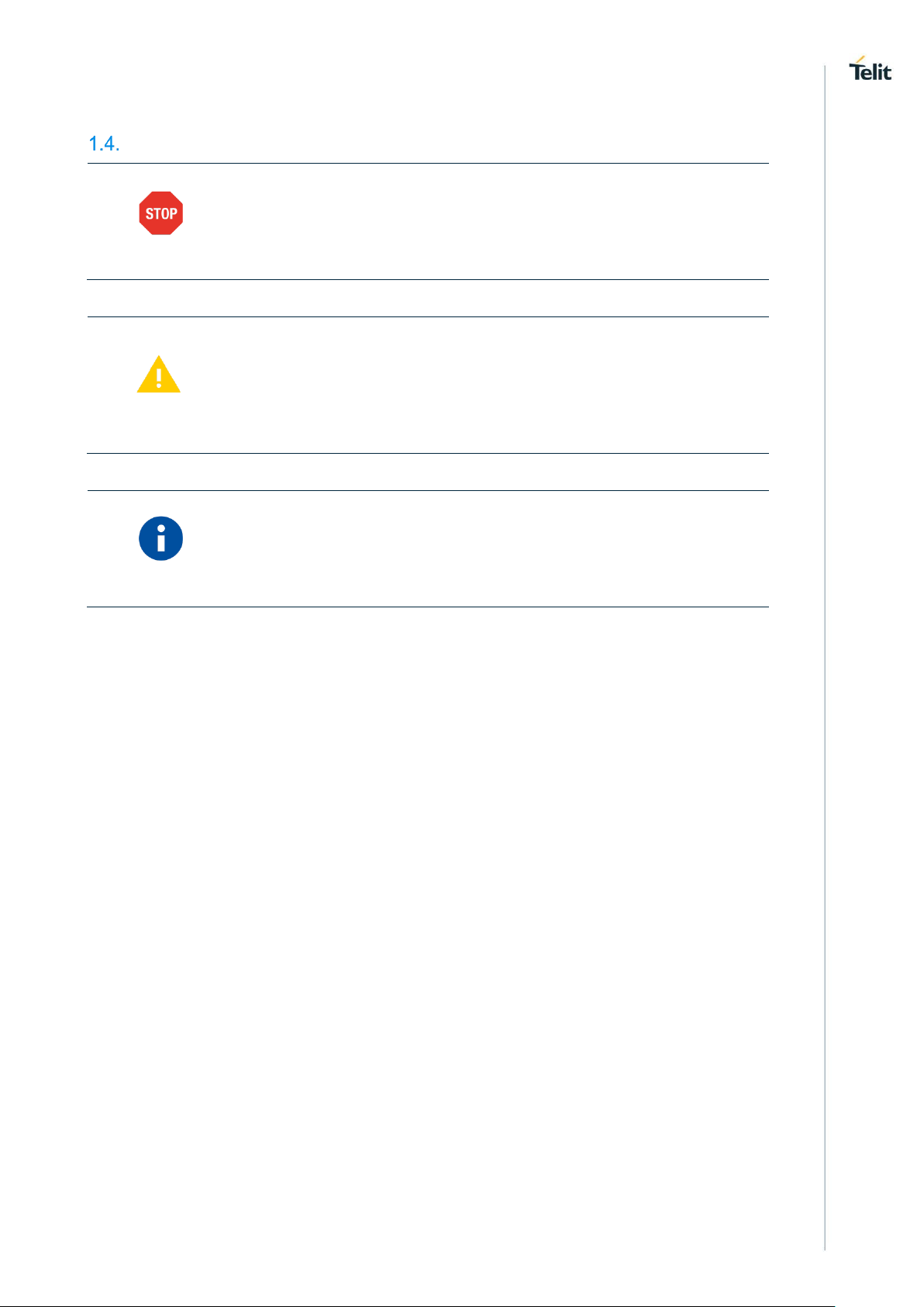
Text Conventions
Danger – This information MUST be followed or catastrophic
equipment failure or bodily injury may occur.
Caution or Warning – Alerts the user to important points about
integrating the module, if these points are not followed, the module and
end user equipment may fail or malfunction.
Tip or Information – Provides advice and suggestions that may be
useful when integrating the module.
All dates are in ISO 8601 format, i.e. YYYY-MM-DD.
Page 12

LE910Cx mPCIe HW Design Guide
1VV0301510 Rev. 4 Page 12 of 79 2018-06-26
Related Documents
[1] LE910C1 Hardware User Guide 1VV0301298
[2] LE920x4/LE910Cx AT Command User Guide 80490ST10778A
[3] Telit EVB User Guide 1VV0301249
[4] mPCIe_IFBD_HW_USER_GUIDE 1VV0301483
[5] LE910/LE920 Digital Voice Interface Application Note 80000NT11246A
[6] Event Monitor Application Note 80000NT10028a
[7] PCI Express Mini Card Electromechanical Specification Revision 2.1
Page 13

LE910Cx mPCIe HW Design Guide
1VV0301510 Rev. 4 Page 13 of 79 2018-06-26
2. GENERAL PRODUCT DESCRIPTION
Overview
The aim of this document is to present possible and recommended hardware solutions
useful for developing a product with the Telit LE910Cx-mPCIe module.
LE910Cx-mPCIe is Telit platform for Mini PCIe applications, such as M2M applications,
industrial mobile router and table PC, based on the following technologies:
• LTE / WCDMA networks for data communication
• Designed for industrial grade quality
In its most basic use case, LE910Cx-mPCIe can be applied as a wireless communication
front-end for mobile router products, offering mobile communication features to an
external host CPU through its rich interfaces. LE910Cx-mPCIe can further support
customer software applications and security features. LE910Cx-mPCIe
provides a software application development environment with sufficient system resources
for creating rich on-board applications. Thanks to a dedicated application processor and
embedded security resources, product developers and manufacturers can create products
that guarantee fraud prevention and tamper evidence without extra effort for additional
security precautions. LE910Cx-mPCIe is available in hardware and band variants as listed
in 2.2 Product Variants and Frequency Bands.
Page 14
LE910Cx mPCIe HW Design Guide
1VV0301510 Rev. 4 Page 14 of 79 2018-06-26
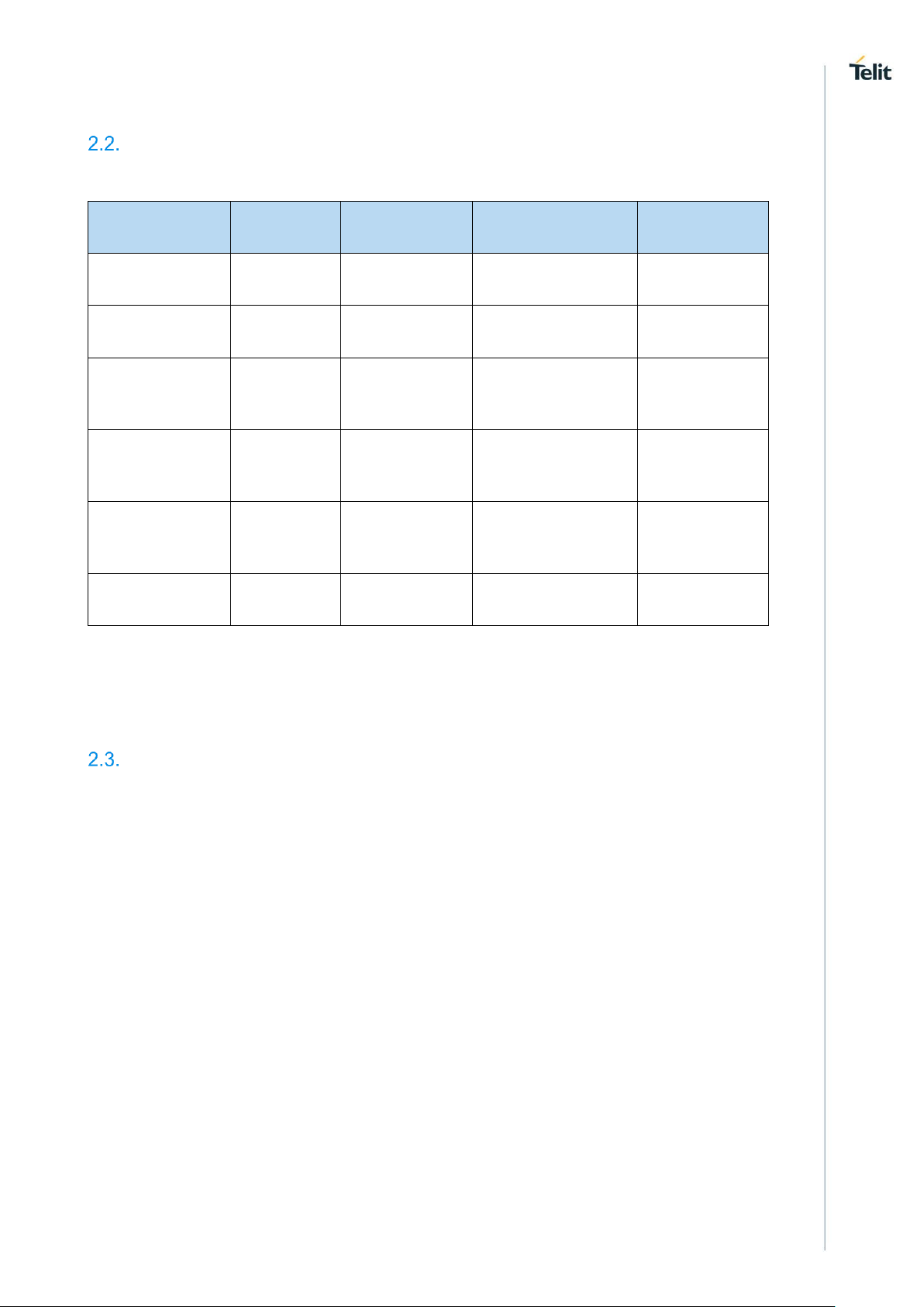
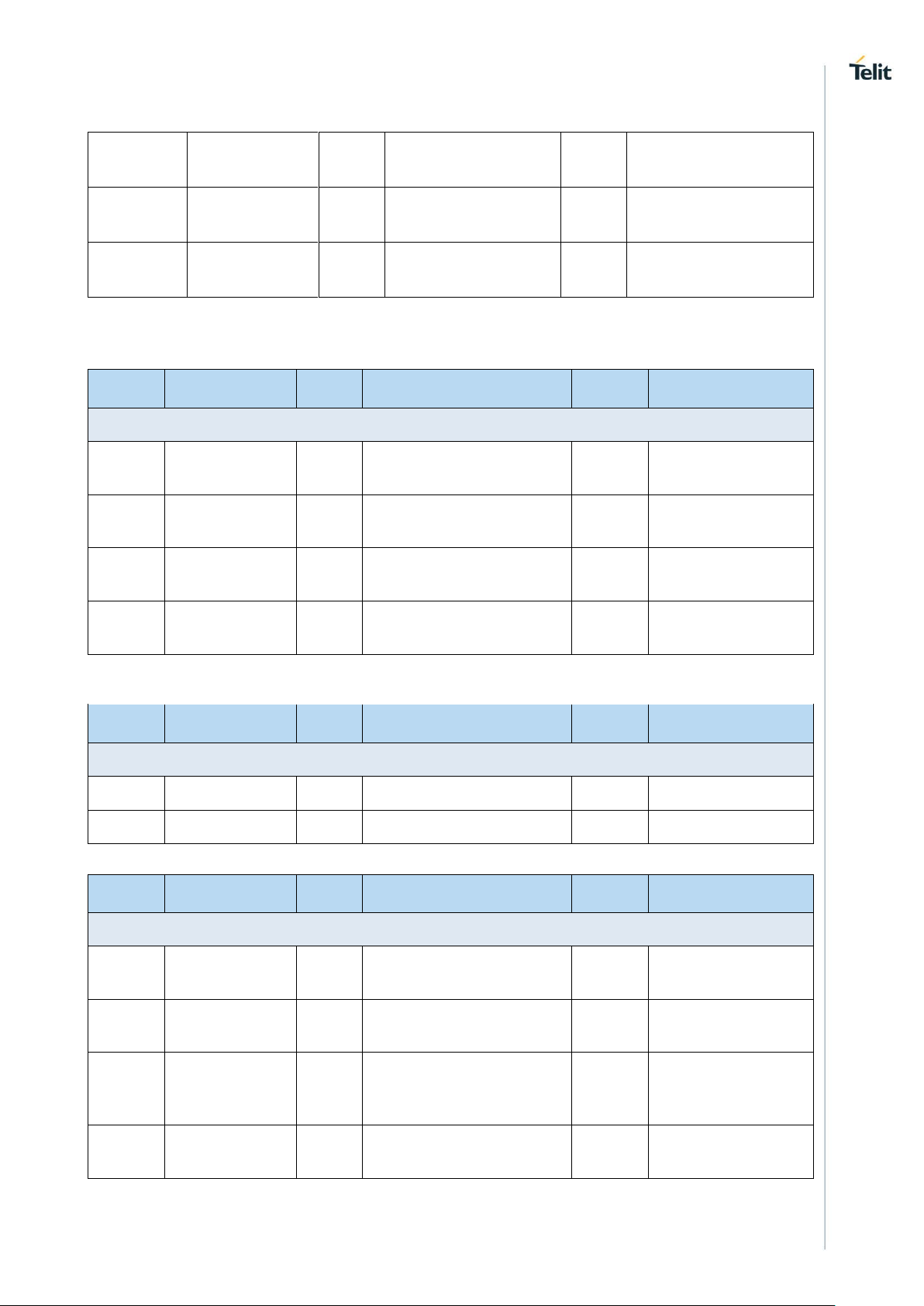
Product Variants and Frequency Bands
LE910Cx modules bands combinations are listed below:
Product
2G Band
3G Band
4G Band
Region
LE910C1-NA
2, 3, 5, 8
1, 2, 4, 5, 8
2, 4, 12
North America
LE910C1-AP
-
1, 5, 8
1, 3, 5, 8, 28
Asia-Pacific
LE910C1-NS
- - 2, 4, 5, 12, 25, 26
North America
- Sprint
LE910C4-NF
-
2, 4, 5
2, 4, 5, 12, 13, 14,
66, 71
North America
LE910C1-NF
-
2, 4, 5
2, 4, 5, 12, 13, 14,
66, 71
North America
LE910C1-EU
3, 8
1, 3, 8
1, 3, 7, 8, 20, 28A
Europe
Table 1 Product Variants and Frequency Bands
Refer to Chapter Reference Table of RF Bands Characteristics 14 for details information
about frequencies and bands.
Target market
LE910Cx-mPCIe can be used for wide variety applications, where low power consumption
and low cost are required while sufficient data rates are achieved:
• Mini PCIe applications
• Mobile router
• Notebook PC
• M2M applications
Page 15
LE910Cx mPCIe HW Design Guide
1VV0301510 Rev. 4 Page 15 of 79 2018-06-26
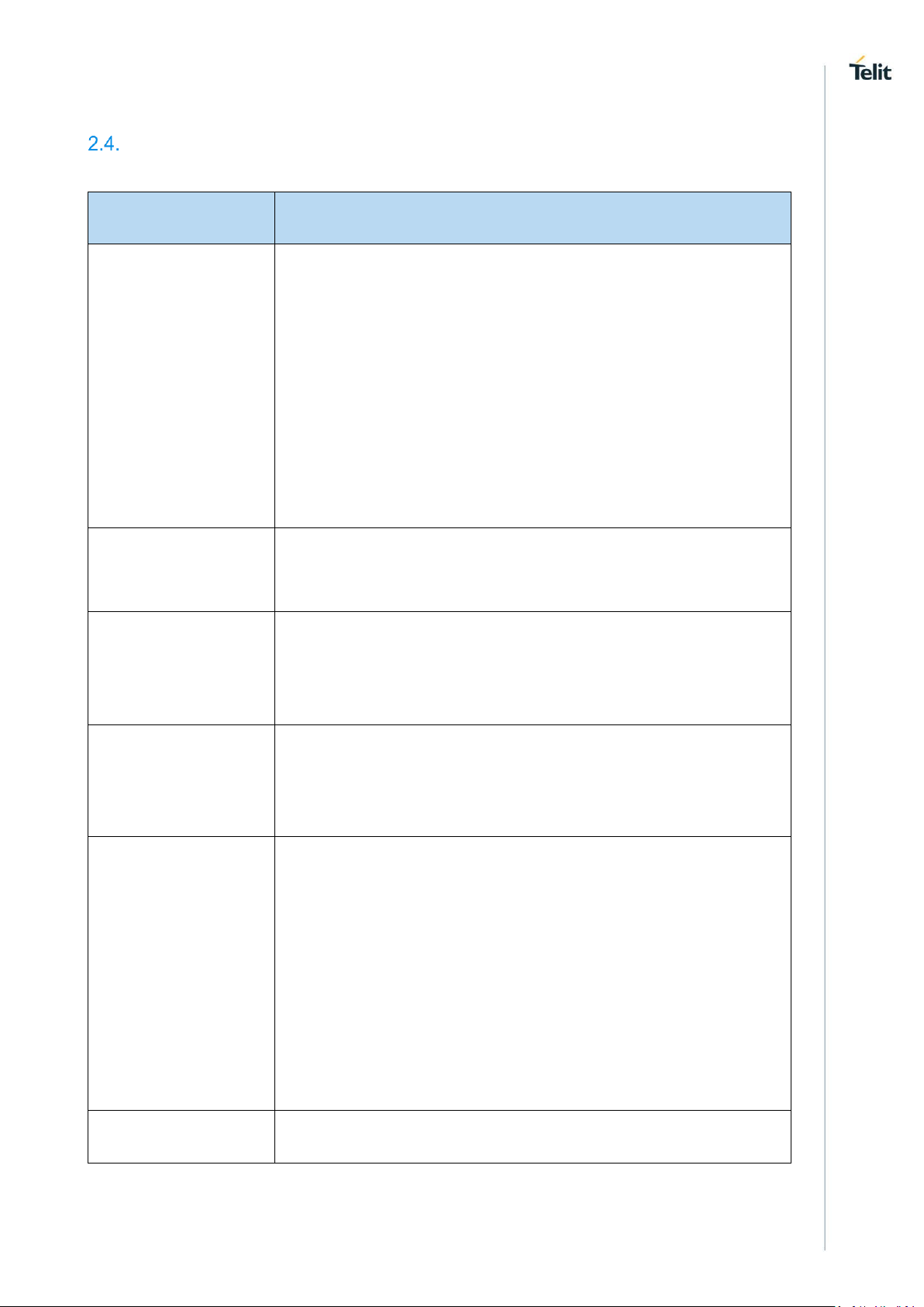
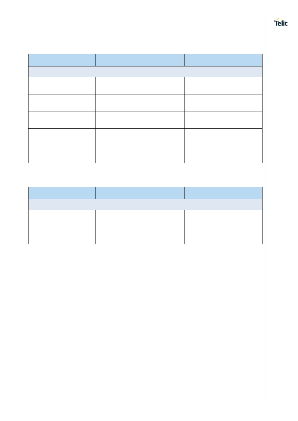
Main features
Function
Features
Modem
• Multi-RAT cellular modem for voice and data communication
• LTE FDD Catx data rates per the module variant used.
• Carrier aggregation is not supported
• GSM/GPRS/EDGE
• WCDMA up to DC HSPA+, Rel.9
• Regional variants with optimal choice of RF bands
• coverage of countries and MNOs
• State-of-the-art GNSS solution with
GPS/GLONASS/BeiDou/Galileo/QZSS receiver
Digital audio
subsystem
• PCM/I2S digital audio interface
• Up to 48 kHz sample rate, 16 bit words
USIM ports – dual
voltage
• Class B and Class C support
• Hot swap support
• Clock rates up to 4 MHz
Application
processor
Application processor to run customer application code
• 32 bit ARM Cortex-A7 up to 1.3 GHz running the Linux operating
system
• Flash + DDR are large enough to allow for customer’s own
software applications
Interfaces
• USB2.0 – USB port is typically used for:
• Flashing of firmware and module configuration
• Production testing
• Accessing the Application Processor’s file system
• AT command access
• High-speed WWAN access to external host
• Diagnostic monitoring and debugging
• Communication between Java application environment
and an external host CPU
• NMEA data to an external host CPU
• Peripheral Ports – I2C, UART
• GPIOs
• Antenna ports
Form factor
Full-Mini Card 52 pin, 50.95mm x 30mm x 1mm.
Page 16

LE910Cx mPCIe HW Design Guide
1VV0301510 Rev. 4 Page 16 of 79 2018-06-26
Environment and
quality requirements
The entire module is designed and qualified by Telit for satisfying
the environment and quality requirements.
Single supply
module
The module generates all its internal supply voltages.
RTC
No dedicated RTC supply, RTC is supplied by VBATT
Table 2 Main features
Page 17
LE910Cx mPCIe HW Design Guide
1VV0301510 Rev. 4 Page 17 of 79 2018-06-26
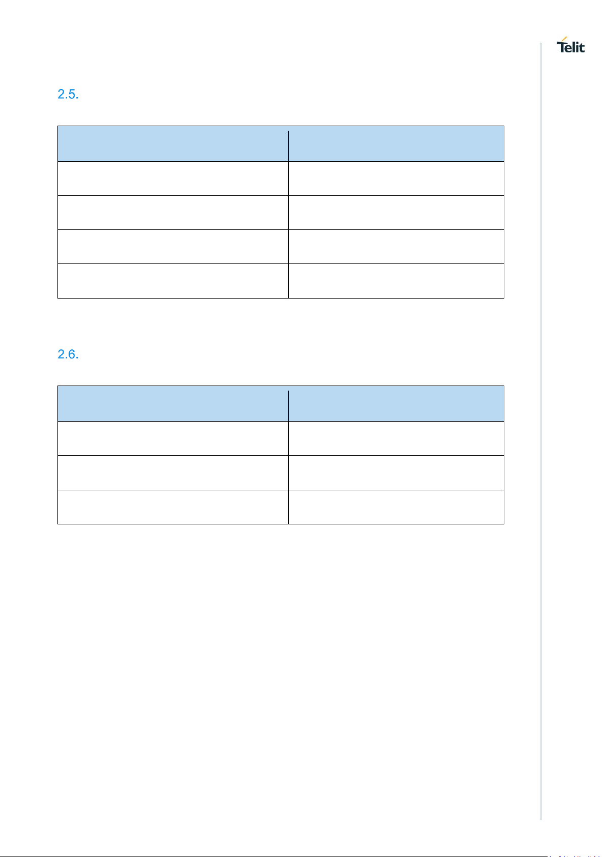
TX Output Power
Technology
Power (dBm)
2G LB
32
2G HB
29
3G/TD-SCDMA
23
4G FDD
22 @1RB
Table 3 TX Output Power
RX Sensitivity
Technology
Sensitivity (dBm)
2G
-107
3G/TD-SCDMA
-112
4G FDD (BW=5 MHz)
-102
Table 4 RX Sensitivity
Page 18

LE910Cx mPCIe HW Design Guide
1VV0301510 Rev. 4 Page 18 of 79 2018-06-26
Mechanical specifications
2.7.1. Dimensions
The overall dimensions of LE910Cx-mPCIe family are:
Length: 50.95 mm
Width: 30 mm
Thickness : 3.2 mm (Version with SIM holder : 4.62 mm)
2.7.2. Weight
The nominal weight of the module is 7 grams.
Page 19
LE910Cx mPCIe HW Design Guide
1VV0301510 Rev. 4 Page 19 of 79 2018-06-26
Temperature range
Case
Range
Note
Operating
Temperature
Range
–20°C ÷ +55°C
The module is fully functional(*) in all the
temperature range, and it fully meets the
3GPP specifications.
–40°C ÷ +85°C
The module is fully functional (*) in all the
temperature range.
However, there may be some
performance deviations in this extended
range relative to 3GPP requirements,
which means that some RF parameters
may deviate from the 3GPP specification
in the order of a few dB.
For example: receiver sensitivity or
maximum output power may be slightly
degraded
Storage and nonoperating
Temperature
Range
–40°C ÷ +105°C
Table 5 Temperature range
(*) Functional: the module is able to make and receive calls, data connection and SMS.
Page 20

LE910Cx mPCIe HW Design Guide
1VV0301510 Rev. 4 Page 20 of 79 2018-06-26
3. PINS ALLOCATION
Pin-out
LE910C1 mPCIe Pin out follows the mPCIe specification [7]
Pin
Signal
I/O
Function
Type
Comment
Power Supply
24
3V3
-
3.3V Main Power
Supply
Power
Supply for 3.3V I/O
UART/DVI interface
2
3V3_AUX
-
3.3V Main Power
Supply
Power 39
3V3_AUX
-
3.3V Main Power
Supply
Power 41
3V3_AUX
-
3.3V Main Power
Supply
Power 52
3V3_AUX
-
3.3V Main Power
Supply
Power 4
GND
-
Ground
9
GND
-
Ground
15
GND
-
Ground
18
GND
-
Ground
21
GND
-
Ground
26
GND
-
Ground
27
GND
-
Ground
29
GND
-
Ground
34
GND
-
Ground
35
GND
-
Ground
37
GND
-
Ground
Page 21
LE910Cx mPCIe HW Design Guide
1VV0301510 Rev. 4 Page 21 of 79 2018-06-26
40
GND
-
Ground
43
GND
-
Ground
50
GND
-
Ground
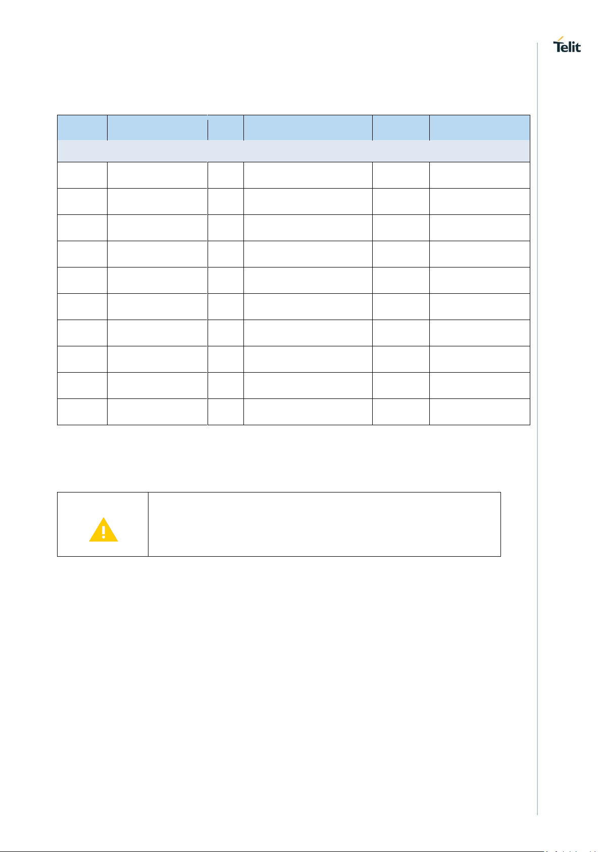
Pin
Signal
I/O
Function
Type
Comment
SIM Card Interface
8
SIMVCC
I/O
External SIM signal –
Power supply for the SIM
1.8 / 3V
10
SIMIO
I/O
External SIM signal Data I/O
1.8 / 3V
12
SIMCLK
O
External SIM signal –
Clock
1.8 / 3V
14
SIMRST
O
External SIM signal –
Reset
1.8 / 3V
Pin
Signal
I/O
Function
Type
Comment
USB Interface
36
USB D-
I/O
USB differential Data (-)
38
USB D+
I/O
USB differential Data (+)
Pin
Signal
I/O
Function
Type
Comment
UART
3
UART_RX
I
Serial data input (RX)
from DTE
1.8V 5
UART_TX
O
Serial data output (TX) to
DTE
1.8V
17
UART_RTS
O
Output Request To
Send signal (RTS) to
DTE
1.8V
19
UART_CTS
I
Input for Clear To Send
signal (CTS) from DTE
1.8V
Page 22
LE910Cx mPCIe HW Design Guide
1VV0301510 Rev. 4 Page 22 of 79 2018-06-26
Pin
Signal
I/O
Function
Type
Comment
Digital Voice Interface (DVI)
45
PCM_CLK
I/O
Digital Audio Interface
(BIT Clock)
1.8V
47
PCM_TX
O
Digital Audio Interface
(TX Out of the card)
1.8V
49
PCM_RX
I
Digital Audio Interface
(RX Into the card)
1.8V
51
PCM_SYNC
I/O
Digital Audio Interface
(Frame_Sync)
1.8V
16
REF_CLK
O
Reference clock for
external Codec
1.8V
Pin
Signal
I/O
Function
Type
Comment
Miscellaneous Functions
30
I2C_SCL
I/O
I2C clock
1.8V
Internally Pull Up
2.2kΩ to 1.8V
32
I2C_SDA
I/O
I2C Data
1.8V
Internally PU 2.2kΩ
to 1.8V
Page 23
LE910Cx mPCIe HW Design Guide
1VV0301510 Rev. 4 Page 23 of 79 2018-06-26
Pin
Signal
I/O
Function
Type
Comment
Miscellaneous Functions
1
WAKE_N
O
Active low output signal
used to wake up the
system from stand-by
3.3V
20
W_DISABLE_N
I
Active low signal for
wireless disabling
(Flight mode)
3.3V
22
PERST_N
I
Active low functional reset
input to the card
3.3V
28
VAUX_PWRMON
O
Supply output for external
accessories /
Power ON monitor
1.8V
42
LED_WWAN_N
O
Active low, open drain
signal for WWAN LED
driving, used to provide
module’s status indication
3.3V
48
GPS_LNA_EN
O
Enables the external
regulator for GPS LNA
1.8V
Page 24
LE910Cx mPCIe HW Design Guide
1VV0301510 Rev. 4 Page 24 of 79 2018-06-26
Table 6 Pin-out
WARNING:
Reserved pins must be left flowting.
Pin
Signal
I/O
Function
Type
Comment
Reserved
6
Reserved -
7
Reserved -
11
Reserved -
13
Reserved -
23
Reserved -
25
Reserved -
31
Reserved -
33
Reserved -
44
Reserved -
46
Reserved -
Page 25

LE910Cx mPCIe HW Design Guide
1VV0301510 Rev. 4 Page 25 of 79 2018-06-26
4. POWER SUPPLY
The power supply circuitry and board layout are a very important part in the full product
design and they strongly reflect on the product overall performances, hence read carefully
the requirements and the guidelines that will follow for a proper design.
Power Supply Requirements
The external power supply must be connected to VBATT signal and must fulfil the
following requirements:
Table 7 Power Supply Requirements
Nominal Supply Voltage
3.3V
Supply Voltage Range
3.1V ~ 3.6V
Max ripple on module input supply
30mV
NOTE:
The Operating Voltage Range MUST never be exceeded; care must be taken
when designing the application’s power supply section to avoid having an
excessive voltage drop.
If the voltage drop is exceeding the limits it could cause a Power Off of the
module.
Overshoot voltage (regarding MAX Extended Operating Voltage) and drop in
voltage (regarding MIN Extended Operating Voltage) MUST never be
exceeded;
The “Extended Operating Voltage Range” can be used only with completely
assumption and application of the HW User guide suggestions.
Power Consumption
For the complete power consumption specification, please refer to the specific Module’s
Hardware User guide listed in section 1.5
Page 26

LE910Cx mPCIe HW Design Guide
1VV0301510 Rev. 4 Page 26 of 79 2018-06-26
General Design Rules
The principal guidelines for the Power Supply Design embrace three different design
steps:
• The electrical design
• The thermal design
• The PCB layout.
4.3.1. Electrical Design Guidelines
The electrical design of the power supply depends strongly from the power source where
this power is drained. We will distinguish them into three categories:
• +5V input (typically PC internal regulator output)
• +12V input (typically automotive)
• Battery
4.3.1.1. +5V Source Power Supply Design Guidelines
• The desired output for the power supply is 3.8V, hence there's not a big difference
between the input source and the desired output and a linear regulator can be
used. A switching power supply will not be suited because of the low drop out
requirements.
• When using a linear regulator, a proper heat sink shall be provided in order to
dissipate the generated heat.
• A Bypass low ESR capacitor of adequate capacity must be provided in order to cut
the current absorption peaks close to the Module, a 100μF capacitor is usually
suited.
• Make sure the low ESR capacitor on the power supply output rated at least 10V.
An example of linear regulator with 5V input is:
Figure 1 linear regulator with 5V input
Page 27

LE910Cx mPCIe HW Design Guide
1VV0301510 Rev. 4 Page 27 of 79 2018-06-26
4.3.1.2. +12V Source Power Supply Design Guidelines
• The desired output for the power supply is 3.8V, hence due to the big difference
between the input source and the desired output, a linear regulator is not suited
and shall not be used. A switching power supply will be preferable because of its
better efficiency.
• When using a switching regulator, a 500kHz or more switching frequency regulator
is preferable because of its smaller inductor size and its faster transient response.
This allows the regulator to respond quickly to the current peaks absorption.
• In any case the frequency and Switching design selection is related to the
application to be developed due to the fact the switching frequency could also
generate EMC interferences.
• For car PB battery the input voltage can rise up to 15,8V and this should be kept in
mind when choosing components: all components in the power supply must
withstand this voltage.
• A Bypass low ESR capacitor of adequate capacity must be provided in order to cut
the current absorption peaks, a 100μF capacitor is usually suited.
• Make sure the low ESR capacitor on the power supply output is rated at least 10V.
For Car applications, a spike protection diode should be inserted close to the
power input, in order to clean the supply from spikes.
An example of switching regulator with 12V input is in the below schematic:
Figure 2 switching regulator 12V
Page 28

LE910Cx mPCIe HW Design Guide
1VV0301510 Rev. 4 Page 28 of 79 2018-06-26
4.3.1.3. Battery Source Power Supply Design Guidelines
The desired nominal output for the power supply is 3.8V and the maximum voltage
allowed is 4.2V, hence a single 3.7V Li-Ion cell battery type is suited for supplying the
power to the Telit LE910Cx Mini PCIe module.
• A Bypass low ESR capacitor of adequate capacity must be provided in order to
cut the current absorption peaks, a 200μF tantalum capacitor is usually suited.
• Make sure the low ESR capacitor (usually a tantalum one) is rated at least 10V.
• A protection diode should be inserted close to the power input, in order to save the
xE910Cx Mini PCIe from power polarity inversion. Otherwise the battery connector
should be done in a way to avoid polarity inversions when connecting the battery.
• The selected battery should be capable of supporting the max peak currents of
~2.4A.
NOTE:
DON'T USE any Ni-Cd, Ni-MH, and Pb battery types directly
connected with xE910Cx Mini PCIe. Their use can lead to
overvoltage on the LE910Cx Mini PCIe and damage it. USE ONLY
Li-Ion battery types.
Page 29

LE910Cx mPCIe HW Design Guide
1VV0301510 Rev. 4 Page 29 of 79 2018-06-26
4.3.2. Thermal Design Guidelines
The thermal design of the application board and the power supply heat sink should be
done with the following specifications:
• Typical average current consumption during xE910Cx Mini PCIe transmission @
Max PWR level at min battery level (LTE) : 700 mA
• Average current during idle (USB enabled): 30 mA
• Average current during idle (USB disabled): 5 mA
• Average current during airplane mode (USB disabled): 2 mA
Considering the very low current during Idle, especially if the Power Saving function is
enabled, it is possible to consider from the thermal point of view that the device absorbs
significant current mainly during Data session. In LTE/WCDMA/HSPA mode, the xE910Cx
Mini PCIe emits RF signals continuously during transmission. Therefore, you must pay
special attention how to dissipate the heat generated.
The LE910Cx mPCIe card is designed to conduct the heat flow from the module IC’s
towards the bottom of the mPCIe PCB across GND metal layers
In order to achieve the best performance, the application board copper layers should be
used to dissipate the heat out of the mPCIe card.
In order to ensure proper thermal flow from the mPCIe card to the application board, the
mPCIe card bottom side should be thermally connected to the application board top side
via proper thermal pad.
The area of which the thermal pad is attached to on the application board must be
designed as a large ground pad (with solder mask exposed).
NOTE:
The average consumption during transmissions depends on the
power level at which the device is requested to transmit by the
network. The average current consumption hence varies significantly.
Page 30

LE910Cx mPCIe HW Design Guide
1VV0301510 Rev. 4 Page 30 of 79 2018-06-26
4.3.3. Power Supply PCB layout Guidelines
The GSM system is made in a way that the RF transmission is not continuous, else it is
packed into bursts at a base frequency of about 216 Hz, and the relative current peaks
can be as high as about 2.4A. Therefore the power supply has to be designed in order to
withstand with these current peaks without big voltage drops; this means that both the
electrical design and the board layout must be designed for this current flow. If the voltage
drop during the peak current absorption is too much, then the device may even shutdown
as a consequence of the supply voltage drop.
NOTE:
The electrical design for the Power supply should be made ensuring
it will be capable of a peak current output of at least 2.4 A.
As seen on the electrical design guidelines the power supply shall have a low ESR
capacitor on the output to cut the current peaks on the input to protect the supply from
spikes. The placement of this component is crucial for the correct working of the circuitry.
A misplaced component can be useless or can even decrease the power supply
performances.
• The Bypass low ESR capacitor must be placed close to the Telit LE910C1-mPCIe
power input pads or in the case the power supply is a switching type it can be
placed close to the inductor to cut the ripple provided the PCB trace from the
capacitor to the LE910C1-MPCIE is wide enough to ensure a dropless connection
even during an 1A current peak.
• The protection diode must be placed close to the input connector where the power
source is drained.
• The PCB traces from the input connector to the power regulator IC must be wide
enough to ensure no voltage drops occur when a 1A current peak is absorbed.
• The PCB traces to the LE910Cx-mPCIE and the Bypass capacitor must be wide
enough to ensure no significant voltage drops occur. This is for the same reason
as previous point. Try to keep this trace as short as possible.
• To reduce the EMI due to switching, it is important to keep very small the mesh
involved; thus the input capacitor, the output diode (if not embodied in the IC) and
the regulator have to form a very small loop. This is done in order to reduce the
radiated field (noise) at the switching frequency (100-500 kHz usually).
• A dedicated ground for the Switching regulator separated by the common ground
plane is suggested.
• The placement of the power supply on the board should be done in such a way to
guarantee that the high current return paths in the ground plane are not
overlapped to any noise sensitive circuitry as the microphone amplifier/buffer or
earphone amplifier.
• The power supply input cables should be kept separate from noise sensitive lines
such as microphone/earphone cables.
• The insertion of EMI filter on VBATT pins is suggested in those designs where
antenna is placed close to battery or supply lines.
Page 31

LE910Cx mPCIe HW Design Guide
1VV0301510 Rev. 4 Page 31 of 79 2018-06-26
A ferrite bead like Murata BLM18EG101TN1 or Taiyo Yuden P/N
FBMH1608HM101 can be used for this purpose.
The below figure shows the recommended circuit:
Figure 3 Power supply recommended circuit
Page 32

LE910Cx mPCIe HW Design Guide
1VV0301510 Rev. 4 Page 32 of 79 2018-06-26
VAUX/PWRMON Power Output
A regulated power supply output is provided to supply small devices from the module.
This output is active when the module is ON and goes OFF when the module is shut
down. The operating range characteristics of the supply are as follows:
Table 8 VAUX/PWRMON Power Output
NOTE:
The Output Current MUST never be exceeded; care must be taken
when designing the application section to avoid having an excessive
current consumption.
If the Current is exceeding the limits it could cause a Power Off of the
module.
Warning:
The current consumption from VAUX/PWRMON increases the
modem temperature.
Item
Min
Typical
Max
Output voltage
1.75V
1.80V
1.85V
Output current
100mA
Output bypass capacitor
(inside the module)
1 μF
Page 33

LE910Cx mPCIe HW Design Guide
1VV0301510 Rev. 4 Page 33 of 79 2018-06-26
GNSS LNA BIAS
A dedicated regulated bias is provided to support active antenna GNSS applications. The
operating range characteristics of the supply are as follows:
Table 9 GNSS LNA BIAS
NOTE:
Follow LE9x0 AT Command User Guide 80407ST10116A to control
dedicated enable GPS_LNA_EN (pin 48) for LE910Cx-mPCIe on
board LNA BIAS output through GNSS antenna port.
NOTE:
In case internal bias is not sufficaint, the user can add an external
bias which can be controlled by pin 48 GPS_LNA_EN, using AT
command. In this case a DC block should be used to avoid conflict
with miniPCIe adapter interrnal LDO.
Item
Min
Typical
Max
Output voltage
0V
3V
3.1V
Output current
100mA
Page 34

LE910Cx mPCIe HW Design Guide
1VV0301510 Rev. 4 Page 34 of 79 2018-06-26
5. ELECTRICAL SPECIFICATION
Absolute Maximum Ratings – Not Operational
Caution - A deviation from the value ranges listed below may harm the
LM940 module.
Table 10 Absolute Maximum Ratings – Not Operational
Symbol
Parameter
Min
Max
Unit
VBATT
Battery supply voltage on pin VBATT
-0.5
4.2
[V]
Recommended Operating Conditions
Table 11 Recommended Operating Conditions
Symbol
Parameter
Min
Typ
Max
Unit
T
amb
Ambient temperature
-40
+25
+85
[°C]
VBATT
Battery supply voltage on pin VBATT
3.1
3.3
3.6
[V]
I
VBATT
+
I
VBATT_PA
Peak current to be used to dimension
decoupling capacitors on pin VBATT
-
-
2400
[mA]
Page 35

LE910Cx mPCIe HW Design Guide
1VV0301510 Rev. 4 Page 35 of 79 2018-06-26
6. DIGITAL SECTION
Logic Levels
ABSOLUTE MAXIMUM RATINGS:
Table 12 Absolute Maximum Rating CMOS 1.8V
Table 13 Absolute Maximum Rating CMOS 3.3V
Parameter
Min
Max
Input level on any digital pin (CMOS 1.8) with respect
to ground
-0.3V
2.16V
Input level on any digital pin (CMOS 1.8) with respect
to ground
when VBATT is not supplied
-0.3V
0.3V
Parameter
Min
Max
Input level on any digital pin (CMOS 3.3) with respect
to ground
-0.3V
3.6V
Input level on any digital pin (CMOS 3.3) with respect
to ground
when VBATT is not supplied
-0.3V
0.3V
Page 36

LE910Cx mPCIe HW Design Guide
1VV0301510 Rev. 4 Page 36 of 79 2018-06-26
OPERATING RANGE - INTERFACE LEVELS 1.8V CMOS:
Parameter
Min
Max
Input high level
1.25V
1.95V
Input low level
0V
0.6V
Output high level
1.4V
--
Output low level
--
0.45V
Pull-up resistance
10kΩ
390 [kΩ]
Pull-up resistance
10kΩ
390 [kΩ]
Input capacitance
--
5pF
Low-level input leakage current, no pull-up
-1uA
--
High-level input leakage current, no pull-down
--
+1uA
Drive strength
2mA
16mA
Table 14 Operating Range CMOS 1.8V
OPERATING RANGE - INTERFACE LEVELS 3.3V CMOS:
Parameter
Min
Max
Input high level
2V
3.3V
Input low level
0V
0.8V
Output high level
2V
--
Output low level
--
0.45V
Table 15 Operating Range CMOS 3.3V
Page 37

LE910Cx mPCIe HW Design Guide
1VV0301510 Rev. 4 Page 37 of 79 2018-06-26
OPERATING RANGE - SIM CARD PADS @2.95V:
Parameter
Min
Max
Input high level
2.1V
3.1V
Input low level
-0.3V
0.55V
Output high level
2.25V
3.1V
Output low level
0V
0.4V
Low-level input leakage current, no pull-up
-10uA
High-level input leakage current, no pull-down
10uA
Pull-up resistance
10kΩ
100kΩ
Pull-down resistance
10kΩ
100kΩ
Input capacitance
5pF
Table 16 Operating Range SIM Card Pads
Page 38

LE910Cx mPCIe HW Design Guide
1VV0301510 Rev. 4 Page 38 of 79 2018-06-26
Power On
The LE910Cx-mPCIe will automatically power on as soon as VBATT applied to the
module. The LE910Cx-mPCIe is not yet activated because the SW initialization process of
the module is still in process internally. It takes some time to fully complete the HW and
SW initialization of the module. For this reason, it is impossible to access LE910Cx-PCIe
during the Initialization state. VAUX / PWRMON pin will be then set at the high logic level
when pins and interfaces are configured.
As shown below the LE910Cx-mPCIe becomes operational (in the Activation state) at
least 20 seconds after power is applied:
Figure 4 Power On Timing Diagram
Note:
To turn on the LE910Cx-mPCIe module, the W_DISABLE_N pin
must not be asserted low.
Page 39

LE910Cx mPCIe HW Design Guide
1VV0301510 Rev. 4 Page 39 of 79 2018-06-26
The following flow chart shows the proper turn on procedure:
PWRMON=ON
?
“Modem ON Proc”
START
PWR Supply ON
PWRMON=ON
?
Delay = 8 s
AT Init Sequence
Enter AT<CR>
N
Delay 1s – 5s
Y
Y
N
Y
Delay = 8 sec
N
Start AT CMD
AT Answer in
1sec?
Modem Reset Proc
N
Y
Delay = 20 s
Page 40

LE910Cx mPCIe HW Design Guide
1VV0301510 Rev. 4 Page 40 of 79 2018-06-26
A flow chart showing the AT commands managing procedure is displayed below:
“Start AT CMD”
START
Delay = 300 msec
Enter AT <CR>
Disconnect PWR Supply
AT answer in
1 sec ?
GO TO
“Modem ON Proc.”
“Start AT CMD”
END
Page 41

LE910Cx mPCIe HW Design Guide
1VV0301510 Rev. 4 Page 41 of 79 2018-06-26
Unconditional Restart
To unconditionally restart the LE910Cx-mPCIe, the pad PERST_N (pin 22) must be tied
low for at least 200 milliseconds and then released.
The hardware unconditional Restart must not be used during normal operation of the
device since it does not detach the device from the network. It shall be kept as an
emergency exit procedure to be done in the rare case that the device gets stuck waiting
for some network or SIM responses.
Do not use any pull up resistor on the PERST_N line nor any totem pole digital output.
Using pull up resistor may bring to latch up problems on the LE910Cx-mPCIe.
The line PERST_N must be connected only in open collector configuration; the transistor
must be connected as close as possible to the PERST_N pin.
The unconditional hardware restart must always be implemented on the application board
as the software must be able to use it as an emergency exit procedure.
PIN DESCRIPTION
Signal
Function
I/O
PIN
PERST_N
Active low functional reset to the card
I
22
Table 17 PERST_N
OPERATING LEVELS
The PERST_N line is 3.3V tolerant as specified by PCI Express Mini Card
Electromechanical Specification Revision 2.1 standard.
WARNING:
The hardware unconditional Reset must not be used during normal
operation of the device since it does not detach the device from the
network. It shall be kept as an emergency exit procedure.
Page 42

LE910Cx mPCIe HW Design Guide
1VV0301510 Rev. 4 Page 42 of 79 2018-06-26
A typical circuit for implementing an unconditional reset is shown below:
Figure 5 Recommended Reset driver circuit
NOTE:
Recommended values R2 = 47kΩ, R1 = 10kΩ.
NOTE:
In order to avoid a back powering effect it is recommended to avoid
having any HIGH logic level signal applied to the digital pins of the
LE910Cx-mPCIE when the module is powered off or during a reboot
transition.
Using bidirectional level translators which do not support High Z mode
during power off is not recommended.
Note:
For Unconditional Restart W_DISABLE_N pin must not be asserted
low otherwise the module will shoutdown itself and will not restart
(this can be used as emergency shutdown but not recommended)
For proper shoutdown refer to section Error! Reference source not f
ound. Error! Reference source not found..
Page 43

LE910Cx mPCIe HW Design Guide
1VV0301510 Rev. 4 Page 43 of 79 2018-06-26
In the following flow chart is detailed the proper restart procedure:
Note:
In order to prevent a back powering effect it is recommended to avoid
having any HIGH logic level signal applied to the digital pins of the
LE910Cx-mPCIe when the module is powered OFF or during an
ON/OFF transition.
Using bidirectional level translators which do not support High Z mode
during power off is not recommended.
Modem Reset
Proc.
PERST_N = LOW
Delay 200ms
PERST_N = OPEN
Delay 1s
Apply Power
On Procedure
Page 44

LE910Cx mPCIe HW Design Guide
1VV0301510 Rev. 4 Page 44 of 79 2018-06-26
Power OFF procedure
To turn OFF the LE910Cx-mPCIe module, the W_DISABLE_N pin must be asserted low,
otherwise the module will be power up immediately. For proper shutdown operation use
AT#SHDN command. When a shutdown command is sent, LE910Cx goes into the
finalization state and at the end of the finalization process shuts down PWRMON.
The duration of the finalization state can differ according to the current situation of the
module, so a value cannot be defined.
Usually, it will take more than 15 seconds from sending a shutdown command until
reaching a complete shutdown. The DTE should monitor the status of PWRMON to
observe the actual power-off.
Figure 6 Shutdown by Software Command
WARNING:
Please carefully follow the recommended procedure for Power Off.
Removing the power supply can only be done when the unit has reached
power off state.
Not following the recommended shut-down and power off procedures might
damage the device and consequently void the warranty.
Page 45

LE910Cx mPCIe HW Design Guide
1VV0301510 Rev. 4 Page 45 of 79 2018-06-26
The below flow chart is detailed the proper power OFF procedure:
Note:
Software shutdown feature is not supported on early engeeniring
samples.
Modem Power
OFF Proc.
W_DISABLE_N =
LOW
Delay 200ms
AT#SHDN
Delay 15s
Done
PWRMON is
OFF?
Delay 5s
Page 46

LE910Cx mPCIe HW Design Guide
1VV0301510 Rev. 4 Page 46 of 79 2018-06-26
Control signals
Pin
Signal
I/O
Function
Type
1
WAKE_N
O
Active low signal used to wake up the
system from stand-by
3.3V
20
W_DISABLE_N
I
Active low signal for wireless disabling
(Airplane mode)
3.3V
22
PERST_N
I
Active low functional reset to the card
3.3V
42
LED_WWAN_N
O
Active low, open drain signal for
WWAN LED driving, used to provide
module’s status indication
3.3V
48
GPS_LNA_EN
O
Enables the external regulator for
GPS LNA
1.8V
Table 18 Control signals
6.5.1. WAKE_N
WAKE_N is driven, by default, by the module according the PCI Express Mini Card
Electromechanical Specification Revision 2.1.
NOTE:
WAKE_N is not supported in host using PCI Express Mini Card
Electromechanical Specification Revision 1.1 and below.
NOTE:
WAKE_N signal is not active by default. if desired it can be
configured remapping an event under monitoring through at#evmoni.
for details refer to the at command user guide.
Page 47

LE910Cx mPCIe HW Design Guide
1VV0301510 Rev. 4 Page 47 of 79 2018-06-26
The below picture shows the internal WAKE_N driver
Figure 7 WAKE_N internal driver
WAKE_N output may be connected to an edge sensitive application input (e.g. a
microcontroller input with IRQ enabled). No external pull-up is needed, since it is internally
implemented.
EXAMPLE: In the following example, a RING monitor activates the WAKEUP signal. (For
more information read Event Monitor Application Note 80000NT10028a).
AT#ENAEVMONI=0 //disable all events
AT#GPIO=3,0,1 //Set GPIO3=>’0’, “WAKE signal reset”
AT#ENAEVMONICFG=3,1,2 //AT port setting
AT#EVMONI="RING",0,1,3 //event 0-RING, after 3 rings
AT#EVMONI="RING",0,0,"AT#GPIO=3,1,1" //GPIO3=>’1’, “WAKE signal active”
AT#EVMONI=”RING”,1 //event 0-RING enabled
AT#EVMONI="GPIO1",1,1,3 //event 1-GPIO3
AT#EVMONI="GPIO1",1,2,1 //when goes hi
AT#EVMONI="GPIO1",1,3,5 //after 5s
AT#EVMONI="GPIO1",1,0," AT#GPIO=3,0,1" //Set GPIO3=>’0’, “WAKE signal
///reset”
AT#EVMONI="GPIO1",1 //event 1-GPIO3 enabled
AT#ENAEVMONI=1 //enable all events
Page 48

LE910Cx mPCIe HW Design Guide
1VV0301510 Rev. 4 Page 48 of 79 2018-06-26
6.5.2. W_DISABLE_N
W_DISABLE_N is used to force the module into airplane mode. Thanks to its internal pullup, leaving this pin unconnected allows the module to operate normally. This switch
follows the behavior as described in the PCI Express Mini Card Electromechanical
Specification Revision 2.1.
6.5.3. LED_WWAN_N
LED_WWAN# is driven, by default, by the module according the PCI Express Mini Card
Electromechanical Specification Revision 2.1. If desired, LED behavior can be configured
by adjusting software settings. The following picture shows the internal LED_WWAN_N
driver and recommended connection to a LED:
Figure 8 LED_WWAN_N internal driver
NOTE:
THIS SIGNAL IS NOT ACTIVE BY DEFAULT. REFER TO AT#SLED
DESCRIPTION IN THE AT COMMAND USER GUIDE
Page 49

LE910Cx mPCIe HW Design Guide
1VV0301510 Rev. 4 Page 49 of 79 2018-06-26
6.5.4. PERST_N
PERST_N is used to reset the LE910Cx-mPCIe. Whenever this signal is pulled low, the
LE910Cx-mPCIe is reset. When the device is reset it stops any operation. After the
release of the reset the LE910Cx is unconditionally restarted, without doing any detach
operation from the network where it is registered. The reset signal must not be used to
normally restart the device, but only as an emergency exit in the rare case the device
remains stuck waiting for some network response.
PERST_N is internally controlled on start-up to achieve a proper power-on reset
sequence, so there's no need to control this pin on start-up. It may only be used to reset a
device already on that is not responding to any command.
NOTE:
Do not use this signal to power cycle the LE910Cx-mPCIe. Use the
AT#SHDN command instead.
Parameter
Min
Max
PERST_N Input high
2.0V
3.6V
PERST_N Input low
-0.5V
0.8V
Table 19 PERST_N operating levels
Page 50

LE910Cx mPCIe HW Design Guide
1VV0301510 Rev. 4 Page 50 of 79 2018-06-26
Hardware Interfaces
Following table below summarize the hardware interfaces for LE910C1-mPCIe:
Interface
LE910C1-mPCIe
USB
USB2.0
I2C
For sensors, audio control
UART
HS-UART (up to 4 Mbps)
Audio I/F
I2S/PCM
USIM
Dual voltage (1.8V/2.85V)
Antenna ports
2 for Cellular, 1 for GNSS
Table 20 Hardware Interfaces
6.6.1. USB Port
The LE910Cx-mPCIe module includes a Universal Serial Bus (USB) transceiver, which
operates at USB high-speed (480 Mbits/sec). It can also operate with USB full-speed
hosts (12 Mbits/sec).
It is compliant with the USB 2.0 specification and can be used for control and data
transfers as well as for diagnostic monitoring and firmware update.
The USB port is typically the main interface between the LE910Cx-mPCIe module and
OEM hardware.
NOTE:
The USB_D+ and USB_D- signals have a clock rate of 480 MHz. The
signal traces must be routed carefully. Minimize trace lengths, number
of vias, and capacitive loading. The impedance value should be as
close as possible to 90 Ohms differential.
Page 51

LE910Cx mPCIe HW Design Guide
1VV0301510 Rev. 4 Page 51 of 79 2018-06-26
Table Below lists the USB interface signals:
Signal
Pin No
Usage
USB_D-
36
Minus (-) line of the differential, bi-directional USB
signal to/from the peripheral device
USB_D+
38
Plus (+) line of the differential, bi-directional USB
signal to/from the peripheral device
Table 21 USB Interface
NOTE:
USB_VBUS controlled internally by TGPIO_10. For
disabling/enabling use at commands via UART port. For example:
at#gpio=10,0,1 will disable USB_VBUS
at#gpio=10,1,1 will ebable USB_VBUS
For more information follow 80407ST10116A, LE9x0 AT Command
User Guide.
NOTE:
Even if USB communication is not used, it is still highly
recommended to place an optional USB connector on the application
board. At least test points of the USB signals are required since the
USB physical communication is needed in the case of SW update.
Page 52

LE910Cx mPCIe HW Design Guide
1VV0301510 Rev. 4 Page 52 of 79 2018-06-26
6.6.2. Serial Port
The serial port is typically a secondary interface between the LE910Cx-mPCIe module
and OEM hardware. MODEM SERIAL PORT 1(Main) is available on LE910Cx-mPCIe
adaptor
Several configurations can be designed for the serial port on the OEM hardware.
The most common configurations are:
• RS232 PC com port
• Microcontroller UART @ 1.8V (Universal Asynchronous Receive Transmit)
• Microcontroller UART @ 3.3V/5V or other voltages different from 1.8V
Depending on the type of serial port on the OEM hardware, a level translator circuit may
be needed to make the system operate. The only configuration that does not need level
translation is the 1.8V UART.
The levels for LE910C1 UART are the CMOS levels as described in 6.1 Logic Levels
6.6.2.1. Modem Serial Port 1 Signals
Serial Port 1 on LE910Cx-mPCIe is a +1.8V UART with 4 RS232 signals. It differs from
the PC-RS232 in signal polarity (RS232 is reversed) and levels.
List of the signals of LE910Cx-mPCIe serial port:
RS232 Pin
No.
Signal
Pin No.
Name
Usage
2
RXD UART_TX
5
Transmit line
Output transmit line of the
LE910Cx-mPCIe UART
3
TXD UART_RX
3
Receive line
Input receive line of the
LE910Cx-mPCIe UART
5
GND
4,9,15….
Ground
Ground
7
RTS UART_CTS
19
Request to
Send
Input to LE910Cx-mPCIe
controlling the Hardware
flow control
8
CTS UART_RTS
17
Clear to Send
Output from LE910CxmPCIe controlling the
Hardware flow control
Table 22 Modem Serial Port 1 Signals
Page 53

LE910Cx mPCIe HW Design Guide
1VV0301510 Rev. 4 Page 53 of 79 2018-06-26
NOTE:
To avoid a back-powering effect, it is recommended to avoid having
any HIGH logic level signal applied to the digital pins of the module
when it is powered OFF or during an ON/OFF transition.
NOTE:
For minimum implementations, only the TXD and RXD lines need be
connected. The other lines can be left open provided a software flow
control is implemented.
6.6.2.2. RS232 Level Translation
To interface the LE910Cx-mPCIe with a PC com port or a RS232 (EIA/TIA-232)
application, a level translator is required. This level translator must:
• Invert the electrical signal in both directions
• Change the level from 0/1.8V to +15/-15V
The RS232 UART 16450, 16550, 16650 & 16750 chipsets accept signals with lower levels
on the RS232 side (EIA/TIA-562), allowing a lower voltage-multiplying ratio on the level
translator. Note that the negative signal voltage must be less than 0V and hence some
sort of level translation is always required.
The simplest way to translate the levels and invert the signal is by using a single chip-level
translator. There are a multitude of them, differing in the number of drivers and receivers
and in the levels (be sure to get a true RS232 level translator, not a RS485 or other
standards).
By convention, the driver is the level translator from the 0-1.8V UART to the RS232 level.
The receiver is the translator from the RS232 level to 0-1.8V UART.
To translate the whole set of control lines of the UART, the following is required:
• 1 driver
• 1 receiver
Page 54

LE910Cx mPCIe HW Design Guide
1VV0301510 Rev. 4 Page 54 of 79 2018-06-26
NOTE:
The digital input lines operating at 1.8V CMOS therefore, the level
translator IC must not be powered by the +3.8V supply of the module.
Instead, it must be powered from a dedicated +1.8V power supply.
RS232 Level Adaption Circuitry Example:
Figure 9 Level Adapter Example
NOTE:
In this case, the length of the lines on the application must be taken
into account to avoid problems in the case of High-speed rates on
RS232.
The RS232 serial port lines are usually connected to a DB9 connector as shown in a
Figure below. Signal names and directions are named and defined from the DTE point of
view. RS232 Serial Port Lines Connection Layout:
Figure 10 RS232 DB-9 pinout
Page 55

LE910Cx mPCIe HW Design Guide
1VV0301510 Rev. 4 Page 55 of 79 2018-06-26
6.6.3. I2C - Inter-integrated Circuit
The LE910Cx-mPCIe supports an I2C interface on the following pins:
• Pin 30 - I2C_SCL
• Pin 32 - I2C_SDA
The I2C can also be used externally by the end customer application.
LE910Cx-mPCIe supports I2C Master Mode only.
NOTE:
Both I2C lines pulled up internally 2.2kΩ to 1.8V.
6.6.4. Digital Audio
The LE910Cx-mPCIe module can be connected to an external codec through the digital
interface.
The product provides a single Digital Audio Interface (DVI) on the following pins:
Digital Audio Interface (DVI) Signals:
Pin
Signal
I/O
Function
Type
COMMENT
51
PCM_SYNC
I/O
Digital Audio
Interface (WAO)
B-PD 1.8V
PCM_SYNC
49
PCM_RX
I
Digital Audio
Interface (RX)
B-PD 1.8V
PCM_DIN
47
PCM_TX
O
Digital Audio
Interface (TX)
B-PD 1.8V
PCM_DOUT
45
PCM_CLK
I/O
Digital Audio
Interface (CLK)
B-PD 1.8V
PCM_CLK
16
REF_CLK
O
Audio Master
Clock
B-PD 1.8V
I2S_MCLK
Table 23 Digital Audio Interface
Page 56

LE910Cx mPCIe HW Design Guide
1VV0301510 Rev. 4 Page 56 of 79 2018-06-26
LE910Cx-mPCIe DVI has the following characteristics:
• PCM Master mode or Slave mode using short or long frame sync modes
• 16 bit linear PCM format
• PCM clock rates of 256 kHz, 512 kHz, 1024 kHz and 2048 kHz (Default)
• Frame size of 8, 16, 32, 64, 128 & 256 bits per frame
• Sample rates of 8 kHz and 16 kHz
In addition to the DVI port, the LE910Cx-mPCIe module provides a master clock signal
(REF_CLK on Pin 16) which can either provide a reference clock to an external codec or
form an I2S interface together with the DVI port where the REF_CLK acts as the
I2S_MCLK.
The REF_CLK default frequency is 12.288 MHz.
When using the DVI with REF_CLK as an I2S interface, 12.288 MHz is 256 x fs (where fs
= 48 kHz).
For timing diagrams refer to LE910Cx module Hardware Design Guide at 1.5
Page 57

LE910Cx mPCIe HW Design Guide
1VV0301510 Rev. 4 Page 57 of 79 2018-06-26
SIM Interface
The SIM pins provide the connections necessary to interface to a SIM socket located on
the host device. Voltage levels over this interface comply with 3GPP standards. SIMIN
line terminated to GND internally for standard LE910Cx-mPCIe variant without either SIM
holder or onboard eSIM.
Figure 11 SIM Interface
Table 24 SIM Interface signals
NOTE:
The resistor value on SIMIO pulled up to SIMVCC should be defined
accordingly in order to be compliant with 3GPP specification.
LE910Cx-mPCIe contains an internal pull-up resistor on SIMIO.
However, the un-mounted option in the application design can be
recommended in order to tune R1 if necessary.
Pin
Signal
I/O
Function
Type
8
SIMVCC
O
External SIM signal – Power supply for the SIM
1.8 / 3V
10
SIMIO
I/O
External SIM signal - Data I/O
1.8 / 3V
12
SIMCLK
O
External SIM signal – Clock
1.8 / 3V
14
SIMRST
O
External SIM signal – Reset
1.8 / 3V
C1
Not mounted
R1
14
12
SIMCLK
SIMRST
SIMVCC
LE910C1-mPCIe
SIMIN
8
7
SIMIN
1
2
3
4
5
8
SIMIO
6
External SIM card
8.2K
GND
GND
GND
10
C2
C3
C4
100nF
33pF
33pF
33pF
Page 58

LE910Cx mPCIe HW Design Guide
1VV0301510 Rev. 4 Page 58 of 79 2018-06-26
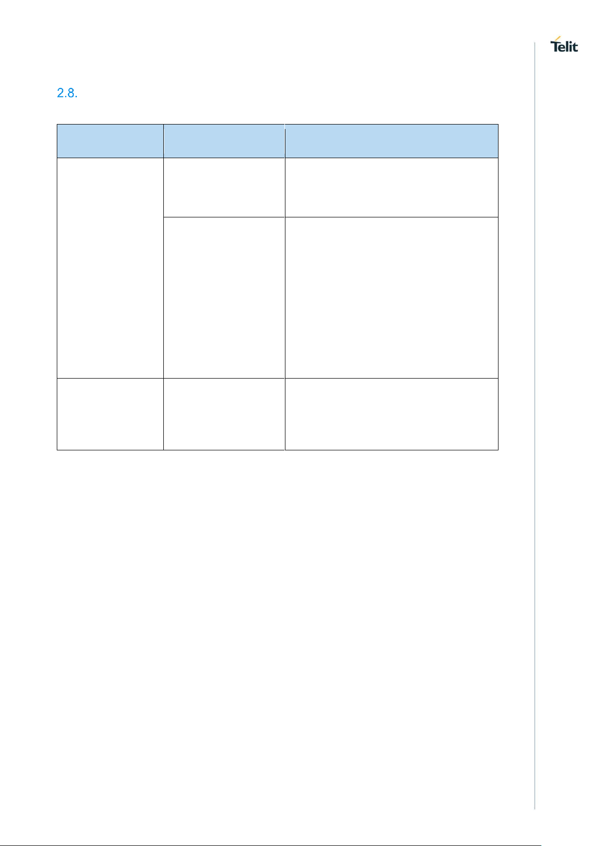
7. RF SECTION
Bands Variants
Please refer to the table provided in section 2.2
TX and RX characteristics
Please refer to the Module’s Hardware User guide for the details
Antenna requirements
7.3.1. Antenna Connectors
The LE910Cx Mini PCIe adapter is equipped with a set of 50 Ω RF U.FL. connectors from
Hirose U.FL-R-SMT-1(10).
The available connectors are:
• RX Diversity Antenna (DIV)
• Main RF antenna (ANT)
• GNSS Antenna (GPS)
See the picture on the right for their position on the
interface.
The presence of all the connectors is depending
on the product characteristics and supported
functionalities.
For more information about mating connectors,
visit the website
http://www.hirose-connectors.com/
Figure 12 UFL Antenna Connectors
The antenna connection is one of the most important aspect in the full product design as it
strongly affects the product overall performances, hence read carefully and follow the
requirements and the guidelines for a proper design.
The LE910Cx-mPCIe adapter is provided with three RF connectors.
The available connectors are:
• Main RF antenna (ANT)
• RX Diversity Antenna (DIV)
• GNSS Antenna (GPS)
Page 59

LE910Cx mPCIe HW Design Guide
1VV0301510 Rev. 4 Page 59 of 79 2018-06-26
Connecting cables between the module and the antenna must have 50 Ω impedance.
If the impedance of the module is mismatched, RF performance is reduced significantly.
If the host device is not designed to use the module’s diversity or GPS antenna, terminate
the interface with a 50Ω load.
7.3.2. Main GSM/WCDMA/LTE Antenna Requirements
The antenna for the LE910C1-mPCIe device must meet the following requirements:
Table 25 Main Antenna Requirements
Item
Value
Frequency range
The customer must use the most suitable antenna band width
for covering the frequency bands provided by the network
operator while using the Telit module.
The bands supported by each variant of the xE910Cx module
family are provided in Section 2.2 Product Variants and
Frequency Bands
Gain
Gain < 3 dBi
Impedance
50 ohm
Input power
> 33 dBm(2 W) peak power in GSM
> 24 dBm average power in WCDMA & LTE
VSWR absolute max
≤ 10:1 (limit to avoid permanent damage)
VSWR recommended
≤ 2:1 (limit to fulfill all regulatory requirements)
Page 60

LE910Cx mPCIe HW Design Guide
1VV0301510 Rev. 4 Page 60 of 79 2018-06-26
7.3.3. Antenna Diversity Requirements
This product includes an input for a second Rx antenna to improve radio sensitivity. The
function is called Antenna Diversity.
Table 26 Diversity Antenna Requirements
The second Rx antenna should not be located in the close vicinity of main antenna. In
order to improve Diversity Gain, Isolation and reduce mutual interaction, the two antennas
should be located at the maximum reciprocal distance possible, taking into consideration
the available space in the application.
7.3.4. GNSS Antenna Requirements
LE910Cx modules supports an active antenna. LNA BIAS provided by onboard 3V,
100mA Linear Regulator. Follow LE9x0 AT Command User Guide 80407ST10116A to
control GPS_LNA_EN (pin 48).
It is recommended to use antennas as follow:
• An external active antenna (17dB typ. Gain, GPS only)
• An external active antenna plus GNSS pre-filter (17dB typ. Gain)
NOTE:
The external GNSS pre-filter is required for the GLONASS application.
The GNSS pre-filter must meet the following requirements:
Source and load impedance = 50 Ohm
• Insertion loss (1575.42–1576.42 MHz) = 1.4 dB (Max)
• Insertion loss (1565.42–1585.42 MHz) = 2.0 dB (Max)
• Insertion loss (1597.5515–1605.886 MHz) = 2.0 dB (Max)
Item
Value
Frequency range
The customer must use the most suitable antenna band
width for covering the frequency bands provided by the
network operator while using the Telit module.
The bands supported by each variant of the xE910Cx
module family are provided in Section 2.2 Product
Variants and Frequency Bands
Impedance
50 ohm
VSWR recommended
≤ 2:1 (limit to fulfill all regulatory requirements)
Page 61

LE910Cx mPCIe HW Design Guide
1VV0301510 Rev. 4 Page 61 of 79 2018-06-26
NOTE:
It is recommended to add a DC block to the customer’s GPS application
to prevent damage to the LE910Cx-mPCIe module due to unwanted DC
voltage.
7.3.4.1. Combined GNSS Antenna
The use of a combined RF/GNSS antenna is NOT recommended. This solution can
generate an extremely poor GNSS reception. In addition, the combination of antennas
requires an additional diplexer, which adds significant power loss in the RF path.
7.3.4.2. Linear and Patch GNSS Antenna
Using this type of antenna introduces at least 3 dB of loss compared to a circularly polarized
(CP) antenna. Having a spherical gain response instead of a hemispherical gain response
can aggravate the multipath behavior and create poor position accuracy.
NOTE:
Please refer to the Module’s Hardware User Guide for detailed
information about GPS operating modes and RF signal requirements.
Page 62

LE910Cx mPCIe HW Design Guide
1VV0301510 Rev. 4 Page 62 of 79 2018-06-26
8. MECHANICAL DESIGN
Mechanical Dimensions
The LE910Cx-mPCIe overall dimensions are:
• Length: 50.95 mm
• Width: 30 mm
• Thickness 3.2 mm (Version with SIM holder : 4.62 mm)
• Weight: 7 gr
8.1.1. Mechanical Drawing
8.1.2. Top View
The figure below shows mechanical top view of the LE910Cx-mPCIe
Figure 13 LE910C1-mPCIe Top View (Dimensions are in mm)
Page 63

LE910Cx mPCIe HW Design Guide
1VV0301510 Rev. 4 Page 63 of 79 2018-06-26
8.1.3. Bottom View
The figure below shows mechanical bottom view of the LE910Cx-mPCIe as seen from
bottom side. The figure shows the SIM holder although by default it is not mounted.
Figure 14 LE910C1-mPCIe Bottom View
Page 64

LE910Cx mPCIe HW Design Guide
1VV0301510 Rev. 4 Page 64 of 79 2018-06-26
8.1.4. Side View
The figure below shows mechanical side view of the LE910Cx-mPCIe.
Figure 15 LE910C1-mPCIe Side View
Page 65

LE910Cx mPCIe HW Design Guide
1VV0301510 Rev. 4 Page 65 of 79 2018-06-26
9. APPLICATION PCB DESIGN
The LE910Cx-mPCIe modules have been designed in order to be compliant with a
standard lead-free SMT process.
Recommended footprint for the application
LE910Cx-mPCIe modules fits any full mPCIe 52 pin socket and latch connectors
compliant with PCI Express Mini Card Electromechanical Specification Revision 2.1
Given below example of board connector (MM60-52B1-E1-R650, JAE) and latch (MM60EZH059-B5-R650, JAE) footprint for reference only:
Figure 16 LE910C1-mPCIe Footprint Reference
Page 66

LE910Cx mPCIe HW Design Guide
1VV0301510 Rev. 4 Page 66 of 79 2018-06-26
10. EMC RECOMMENDATIONS
All LE910Cx-mPCIe signals are provided with some EMC protection. Nevertheless, the
accepted level differs according to the specific pin.
EMC Recommendations:
Table 27 EMC RECOMMENDATIONS
Appropriate series resistors must be considered to protect the input lines from overvoltage.
Pad
Signal
I/O
Function
Contact
Air
All Pins
All pins
All functions
± 4KV
± 8KV
Antenna
Antenna
connectors
Analog
I/O
Antenna connectors
± 4KV
± 4KV
Page 67

LE910Cx mPCIe HW Design Guide
1VV0301510 Rev. 4 Page 67 of 79 2018-06-26
11. PACKING SYSTEM
Tray
The LE910Cx-mPCIe modules are packaged on trays of 20 pieces each:
Modules per
Tray
Trays per
Envelope
Modules per
Envelope
Envelopes per Carton
Box
Modules per
Box
20
5 + 1 empty
100
5
500
Table 28 Tray Packing
Order Type
Quantity
Minimum Order Quantity (MOQ)
20
Standard Packing Quantity (SPQ)
500
Table 29 Packing Quantities
Page 68

LE910Cx mPCIe HW Design Guide
1VV0301510 Rev. 4 Page 68 of 79 2018-06-26
Tray organization is shown in the figure below
Figure 17 LE910C1-mPCIe Tray organization
Page 69

LE910Cx mPCIe HW Design Guide
1VV0301510 Rev. 4 Page 69 of 79 2018-06-26
Tray Drawing
Figure 18 LE910C1-mPCIe Tray Drawing
WARNING:
These trays can withstand a maximum temperature of 65℃.
Page 70

LE910Cx mPCIe HW Design Guide
1VV0301510 Rev. 4 Page 70 of 79 2018-06-26
Moisture sensitivity
The LE910Cx-mPCIe is a Moisture Sensitive Device level 3, in according with standard
IPC/JEDEC J-STD-020, take care all the relatives requirements for using this kind of
components.
Moreover, the customer has to take care of the following conditions:
a) Calculated shelf life in sealed bag: 12 months at <40°C and <90% relative humidity (RH).
b) Environmental condition during the production: 30°C / 60% RH according to IPC/JEDEC
J-STD-033A paragraph 5.
c) The maximum time between the opening of the sealed bag and the reflow process must
be 168 hours if condition b) “IPC/JEDEC J-STD-033A paragraph 5.2” is respected
d) Baking is required if conditions b) or c) are not respected
e) Baking is required if the humidity indicator inside the bag indicates 10% RH or more
Page 71

LE910Cx mPCIe HW Design Guide
1VV0301510 Rev. 4 Page 71 of 79 2018-06-26
12. CONFORMITY ASSESSMENT ISSUES
Declaration of Conformity
Hereby, Telit Communications S.p.A declares that the LE910Cx-mPCIe is in compliance
with Directive 2014/53/EU.
The full text of the EU declaration of conformity is available at the following internet address:
http://www.telit.com\red
Page 72

LE910Cx mPCIe HW Design Guide
1VV0301510 Rev. 4 Page 72 of 79 2018-06-26
13. SAFETY RECOMMENDATIONS
READ CAREFULLY
Be sure the use of this product is allowed in the country and in the environment required.
The use of this product may be dangerous and has to be avoided in the following areas:
• Where it can interfere with other electronic devices in environments such as
hospitals, airports, aircrafts, etc.
• Where there is risk of explosion such as gasoline stations, oil refineries, etc. It is the
responsibility of the user to enforce the country regulation and the specific
environment regulation.
Do not disassemble the product; any mark of tampering will compromise the warranty
validity. We recommend following the instructions of the hardware user guides for correct
wiring of the product. The product has to be supplied with a stabilized voltage source and
the wiring has to be conformed to the security and fire prevention regulations. The product
has to be handled with care, avoiding any contact with the pins because electrostatic
discharges may damage the product itself. Same cautions have to be taken for the SIM,
checking carefully the instruction for its use. Do not insert or remove the SIM when the
product is in power saving mode.
The system integrator is responsible for the functioning of the final product; therefore, care
has to be taken to the external components of the module, as well as any project or
installation issue, because the risk of disturbing the GSM network or external devices or
having impact on the security. Should there be any doubt, please refer to the technical
documentation and the regulations in force. Every module has to be equipped with a proper
antenna with specific characteristics. The antenna has to be installed with care in order to
avoid any interference with other electronic devices and has to guarantee a minimum
distance from the body (20 cm). In case this requirement cannot be satisfied, the system
integrator has to assess the final product against the SAR regulation.
The European Community provides some Directives for the electronic equipment
introduced on the market. All of the relevant information is available on the European
Community website:
http://ec.europa.eu/enterprise/sectors/rtte/documents/
The text of the Directive 99/05 regarding telecommunication equipment is available,
while the applicable Directives (Low Voltage and EMC) are available at:
http://ec.europa.eu/enterprise/sectors/electrical/
Page 73

LE910Cx mPCIe HW Design Guide
1VV0301510 Rev. 4 Page 73 of 79 2018-06-26
14. REFERENCE TABLE OF RF BANDS CHARACTERISTICS
Mode
Freq. Tx
(MHz)
Freq. Rx
(MHz)
Channels
Tx-Rx Offset
PCS 1900
1850.2 ~ 1909.8
1930.2 ~ 1989.8
512 ~ 810
80 MHz
DCS 1800
1710 ~ 1785
1805 ~ 1880
512 ~ 885
95 MHz
GSM 850
824.2 ~ 848.8
869.2 ~ 893.8
128 ~ 251
45 MHz
EGSM 900
890 ~ 915
935 ~ 960
0 ~ 124
45 MHz
880 ~ 890
925 ~ 935
975 ~ 1023
45 MHz
WCDMA 2100 – B1
1920 ~ 1980
2110 ~ 2170
Tx: 9612 ~ 9888
Rx: 10562 ~ 10838
190 MHz
WCDMA 1900 – B2
1850 ~ 1910
1930 ~ 1990
Tx: 9262 ~ 9538
Rx: 9662 ~ 9938
80 MHz
WCDMA 1800 – B3
1710 ~ 1785
1805 ~ 1880
Tx: 937 ~ 1288
Rx: 1162 ~ 1513
95 MHz
WCDMA AWS – B4
1710 ~ 1755
2110 ~ 2155
Tx: 1312 ~ 1513
Rx: 1537 ~ 1738
400 MHz
WCDMA 850 – B5
824 ~ 849
869 ~ 894
Tx: 4132 ~ 4233
Rx: 4357 ~ 4458
45 MHz
WCDMA 900 – B8
880 ~ 915
925 ~ 960
Tx: 2712 ~ 2863
Rx: 2937 ~ 3088
45 MHz
WCDMA 1800 – B9
1750 ~ 1784.8
1845 ~ 1879.8
Tx: 8762 ~ 8912
Rx: 9237 ~ 9387
95 MHz
WCDMA 800 – B19
830 ~ 845
875 ~ 890
Tx: 312 ~ 363
Rx: 712 ~ 763
45 MHz
TDSCDMA 2000 – B34
2010 ~ 2025
2010 ~ 2025
Tx: 10054 ~ 10121
Rx: 10054 ~ 10121
0 MHz
TDSCDMA 1900 – B39
1880 ~ 1920
1880 ~ 1920
Tx: 9404 ~ 9596
Rx: 9404 ~ 9596
0 MHz
LTE 2100 – B1
1920 ~ 1980
2110 ~ 2170
Tx: 18000 ~ 18599
Rx: 0 ~ 599
190 MHz
LTE 1900 – B2
1850 ~ 1910
1930 ~ 1990
Tx: 18600 ~ 19199
80 MHz
Page 74

LE910Cx mPCIe HW Design Guide
1VV0301510 Rev. 4 Page 74 of 79 2018-06-26
Rx: 600 ~ 1199
LTE 1800 – B3
1710 ~ 1785
1805 ~ 1880
Tx: 19200 ~ 19949
Rx: 1200 ~ 1949
95 MHz
LTE AWS – B4
1710 ~ 1755
2110 ~ 2155
Tx: 19950 ~ 20399
Rx: 1950 ~ 2399
400 MHz
LTE 850 – B5
824 ~ 849
869 ~ 894
Tx: 20400 ~ 20649
Rx: 2400 ~ 2649
45 MHz
LTE 2600 – B7
2500 ~ 2570
2620 ~ 2690
Tx: 20750 ~ 21449
Rx: 2750 ~ 3449
120 MHz
LTE 900 – B8
880 ~ 915
925 ~ 960
Tx: 21450 ~ 21799
Rx: 3450 ~ 3799
45 MHz
LTE 1800 – B9
1749.9 ~ 1784.9
1844.9 ~ 1879.9
Tx: 21800 ~ 2149
Rx: 3800 ~ 4149
95 MHz
LTE AWS+ – B10
1710 ~ 1770
2110 ~ 2170
Tx: 22150 ~ 22749
Rx: 4150 ~ 4749
400 MHz
LTE 700a – B12
699 ~ 716
729 ~ 746
Tx : 23010 ~ 23179
Rx : 5010 ~ 5179
30 MHz
LTE 700c – B13
777 ~ 787
746 ~ 756
Tx : 27210 ~ 27659
Rx : 9210 ~ 9659
-31 MHz
LTE 700b – B17
704 ~ 716
734 ~ 746
Tx: 23730 ~ 23849
Rx: 5730 ~ 5849
30 MHz
LTE 800 – B19
830 ~ 845
875 ~ 890
Tx: 24000 ~ 24149
Rx: 6000 ~ 6149
45 MHz
LTE 800 – B20
832 ~ 862
791 ~ 821
Tx: 24150 ~ 24449
Rx: 6150 ~ 6449
-41 MHz
LTE 1500 – B21
1447.9 ~ 1462.9
1495.9 ~ 1510.9
Tx: 24450 ~ 24599
Rx: 6450 ~ 6599
48 MHz
LTE 1900+ – B25
1930 ~ 1995
1850 ~ 1915
Tx: 26040 ~ 26689
Rx: 8040 ~ 8689
80 MHz
LTE 850+ – B26
814 ~ 849
859 ~ 894
Tx: 26690 ~ 27039
Rx: 8690 ~ 9039
45 MHz
LTE 700 – B28
703 ~ 748
758 ~ 803
Tx : 27210 ~ 27659
Rx : 9210 ~ 9659
45 MHz
Page 75

LE910Cx mPCIe HW Design Guide
1VV0301510 Rev. 4 Page 75 of 79 2018-06-26
Table 30 REFERENCE TABLE OF RF BANDS
LTE AWS-3 – B66
1710 ~ 1780
2210 ~ 2200
Tx: 131972-132671
Rx: 66436-67335
400 MHz
LTE600 – B71
663 ~ 698
617 ~ 652
Tx: 133122-133471
Rx: 68568-68935
46 MHz
LTE TDD 2600 – B38
2570 ~ 2620
2570 ~ 2620
Tx: 37750 ~ 38250
Rx: 37750 ~ 38250
0 MHz
LTE TDD 1900 – B39
1880 ~ 1920
1880 ~ 1920
Tx: 38250 ~ 38650
Rx: 38250 ~ 38650
0 MHz
LTE TDD 2300 – B40
2300 ~ 2400
2300 ~ 2400
Tx: 38650 ~ 39650
Rx: 38650 ~ 39650
0 MHz
LTE TDD 2500 – B41M
2555 ~ 2655
2555 ~ 2655
Tx: 40265 ~ 41215
Rx: 40265 ~ 41215
0 MHz
Page 76

LE910Cx mPCIe HW Design Guide
1VV0301510 Rev. 4 Page 76 of 79 2018-06-26
15. ACRONYMS
TTSC
Telit Technical Support Centre
USB
Universal Serial Bus
HS
High Speed
DTE
Data Terminal Equipment
UMTS
Universal Mobile Telecommunication System
WCDMA
Wideband Code Division Multiple Access
HSDPA
High Speed Downlink Packet Access
HSUPA
High Speed Uplink Packet Access
UART
Universal Asynchronous Receiver Transmitter
HSIC
High Speed Inter Chip
SIM
Subscriber Identification Module
SPI
Serial Peripheral Interface
ADC
Analog – Digital Converter
DAC
Digital – Analog Converter
I/O
Input Output
GPIO
General Purpose Input Output
CMOS
Complementary Metal – Oxide Semiconductor
MOSI
Master Output – Slave Input
MISO
Master Input – Slave Output
CLK
Clock
MRDY
Master Ready
Page 77

LE910Cx mPCIe HW Design Guide
1VV0301510 Rev. 4 Page 77 of 79 2018-06-26
Table 31 ACRONYMS
SRDY
Slave Ready
CS
Chip Select
RTC
Real Time Clock
PCB
Printed Circuit Board
ESR
Equivalent Series Resistance
VSWR
Voltage Standing Wave Radio
VNA
Vector Network Analyzer
RED
Radio Equipment Directive
Page 78

LE910Cx mPCIe HW Design Guide
1VV0301510 Rev. 4 Page 78 of 79 2018-06-26
16. DOCUMENT HISTORY
Revision
Date
Changes
1
2018-01-11
First issue
2
2018-02-28
Updated weight
Added note related to Power Down / Off
3
2018-06-11
Section 2.2 – Updated product Variants and Frequency
Bands
Section 3.1 – Updated pinout table
Section 4.3.2 – Updated thermal design guidelines
Section 14 - Updated frequency table
4
2018-06-20
Section 1.5 – Updated reference documents
Section 2.2 – Updated product Variants and Frequency
Bands
Section 4.1 & 5.2 – Updated operating voltage settings
Table 32 DOCUMENT HISTORY
Page 79

Mod.0818 2017-11 Rev.0
 Loading...