

Page 1

GE/GC864-QUAD V2 and GE864-GPS
Hardware User Guide
1vv0300915 Rev.5 – 2011-10-03
Page 2

GE/GC864-QUAD V2 and GE864-GPS Hardware User Guide
1vv0300915 Rev.5 – 2011-10-03
APPLICABILITY TABLE
PRODUCT
GE864-QUAD V2
GE864-GPS
GC864-QUAD V2
GC864-QUAD V2
With SIM Holder
Reproduction forbidden without Telit Communications S.p.A. written authorization - All Rights Reserved. Page 2 of 94
Page 3

GE/GC864-QUAD V2 and GE864-GPS Hardware User Guide
1vv0300915 Rev.5 – 2011-10-03
SPECIFICATIONS SUBJECT TO CHANGE WITHOut Notice
Notice
While reasonable efforts have been made to assure the accuracy of this document, Telit
assumes no liability resulting from any inaccuracies or omissions in this document, or from
use of the information obtained herein. The information in this document has been carefully
checked and is believed to be entirely reliable. However, no responsibility is assumed for
inaccuracies or omissions. Telit reserves the right to make changes to any products described
herein and reserves the right to revise this document and to make changes from time to time
in content hereof with no obligation to notify any person of revisions or changes. Telit does
not assume any liability arising out of the application or use of any product, software, or
circuit described herein; neither does it convey license under its patent rights or the rights of
others.
It is possible that this publication may contain references to, or information about Telit
products (machines and programs), programming, or services that are not announced in your
country. Such references or information must not be construed to mean that Telit intends to
announce such Telit products, programming, or services in your country.
Copyrights
This instruction manual and the Telit products described in this instruction manual may be,
include or describe copyrighted Telit material, such as computer programs stored in
semiconductor memories or other media. Laws in the Italy and other countries preserve for
Telit and its licensors certain exclusive rights for copyrighted material, including the
exclusive right to copy, reproduce in any form, distribute and make derivative works of the
copyrighted material. Accordingly, any copyrighted material of Telit and its licensors
contained herein or in the Telit products described in this instruction manual may not be
copied, reproduced, distributed, merged or modified in any manner without the express
written permission of Telit. Furthermore, the purchase of Telit products shall not be deemed
to grant either directly or by implication, estoppel, or otherwise, any license under the
copyrights, patents or patent applications of Telit, as arises by operation of law in the sale of a
product.
Computer Software Copyrights
The Telit and 3rd Party supplied Software (SW) products described in this instruction manual
may include copyrighted Telit and other 3rd Party supplied computer programs stored in
semiconductor memories or other media. Laws in the Italy and other countries preserve for
Telit and other 3rd Party supplied SW certain exclusive rights for copyrighted computer
programs, including the exclusive right to copy or reproduce in any form the copyrighted
computer program. Accordingly, any copyrighted Telit or other 3rd Party supplied SW
computer programs contained in the Telit products described in this instruction manual may
not be copied (reverse engineered) or reproduced in any manner without the express written
permission of Telit or the 3rd Party SW supplier. Furthermore, the purchase of Telit products
shall not be deemed to grant either directly or by implication, estoppel, or otherwise, any
license under the copyrights, patents or patent applications of Telit or other 3rd Party supplied
SW, except for the normal non-exclusive, royalty free license to use that arises by operation
of law in the sale of a product.
Reproduction forbidden without Telit Communications S.p.A. written authorization - All Rights Reserved. Page 3 of 94
Page 4

GE/GC864-QUAD V2 and GE864-GPS Hardware User Guide
1vv0300915 Rev.5 – 2011-10-03
Usage and Disclosure Restrictions
License Agreements
The software described in this document is the property of Telit and its licensors. It is
furnished by express license agreement only and may be used only in accordance with the
terms of such an agreement.
Copyrighted Materials
Software and documentation are copyrighted materials. Making unauthorized copies is
prohibited by law. No part of the software or documentation may be reproduced, transmitted,
transcribed, stored in a retrieval system, or translated into any language or computer language,
in any form or by any means, without prior written permission of Telit
High Risk Materials
Components, units, or third-party products used in the product described herein are NOT
fault-tolerant and are NOT designed, manufactured, or intended for use as on-line control
equipment in the following hazardous environments requiring fail-safe controls: the operation
of Nuclear Facilities, Aircraft Navigation or Aircraft Communication Systems, Air Traffic
Control, Life Support, or Weapons Systems (High Risk Activities"). Telit and its supplier(s)
specifically disclaim any expressed or implied warranty of fitness for such High Risk
Activities.
Trademarks
TELIT and the Stylized T Logo are registered in Trademark Office. All other product or
service names are the property of their respective owners.
Copyright © Telit Communications S.p.A. 2011.
Reproduction forbidden without Telit Communications S.p.A. written authorization - All Rights Reserved. Page 4 of 94
Page 5

GE/GC864-QUAD V2 and GE864-GPS Hardware User Guide
1vv0300915 Rev.5 – 2011-10-03
Contents
APPLICABILITY TABLE .............................................................................................................................................. 2
1. INTRODUCTION ................................................................................................................................ 8
1.1. S
1.2. A
1.3. C
1.4. D
1.5. T
1.6. R
2. OVERVIEW ...................................................................................................................................... 11
3. GE864-QUAD V2/GPS MECHANICAL DIMENSIONS ......................................................................... 12
3.1. GE864-QUAD V2/GPS .................................................................................................................................... 12
3.2. GC864-QUAD V2 ............................................................................................................................................. 13
3.3. M
3.4. GC864-QUAD V2 M
4. ELECTRICAL CONNECTIONS .......................................................................................................... 15
4.1. GE864-QUAD V2/GPS .................................................................................................................................... 15
4.2. GC864-QUAD V2 ............................................................................................................................................. 22
5. HARDWARE COMMANDS ................................................................................................................ 26
COPE
.................................................................................................................................................................. 8
UDIENCE
ONTACT INFORMATION, SUPPORT
OCUMENT ORGANIZATION
EXT CONVENTIONS
ELATED DOCUMENTS
ECHANICAL VIEW OF TELIT
4.1.1.
4.1.2.
4.2.1.
4.2.2.
............................................................................................................................................................ 8
PIN-OUT .................................................................................................................................................. 15
BGA Balls Layout ..................................................................................................................................... 20
PIN-OUT .................................................................................................................................................. 22
GC864-QUAD V2 Antenna Connector ..................................................................................................... 25
...................................................................................................................... 8
................................................................................................................................ 9
.......................................................................................................................................... 10
...................................................................................................................................... 10
GC864-QUAD V2
ODULE CONNECTIONS
WITH
SIM H
OLDER
.............................................................. 14
...................................................................................................... 14
5.1. T
5.2. T
5.3. H
5.4. T
6. POWER SUPPLY ............................................................................................................................. 36
6.1. P
6.2. P
6.3. G
7. ANTENNA ...................................................................................................................................... 45
7.1. GSM A
7.2. PCB G
URNING ON THE
URNING
ARDWARE UNCONDITIONAL RESTART
URNING
5.4.1.
5.4.2.
OWER SUPPLY REQUIREMENTS
OWER CONSUMPTION
ENERAL DESIGN RULES
6.3.1.
6.3.2.
6.3.3.
6.3.4.
7.1.1.
7.1.2.
7.2.1.
OFF
ON/OFF
GPS Power-up .......................................................................................................................................... 35
GPS Shutdown .......................................................................................................................................... 35
Electrical Design Guidelines .................................................................................................................... 38
Thermal Design Guidelines ...................................................................................................................... 42
Power Supply PCB Layout Guidelines ..................................................................................................... 43
Parameters for ATEX Applications .......................................................................................................... 44
NTENNA
GSM Antenna Requirements ..................................................................................................................... 45
GE864-QUAD V2/GPS GSM Antenna – PCB line Guidelines ................................................................ 46
UIDELINES IN CASE OF
Transmission line design .......................................................................................................................... 47
GE/GC864-QUAD V2
THE
GE/GC864-QUAD V2
THE
(GE864-QUAD V2/GPS
AND
GE864-GPS ............................................................................. 26
AND
GE864 GPS ............................................................................ 30
............................................................................................................ 32
GPS (
ONLY
GE864-GPS) ............................................................................................. 35
........................................................................................................................ 36
....................................................................................................................................... 37
................................................................................................................................... 38
AND
GC864-QUAD V2) ................................................................. 45
FCC
CERTIFICATION
............................................................................................ 47
Reproduction forbidden without Telit Communications S.p.A. written authorization - All Rights Reserved. Page 5 of 94
Page 6

7.2.2.
7.2.3.
7.3. GPS A
7.3.1.
7.3.2.
7.3.3.
7.3.4.
7.3.5.
GE/GC864-QUAD V2 and GE864-GPS Hardware User Guide
1vv0300915 Rev.5 – 2011-10-03
Transmission line measurements .............................................................................................................. 48
GSM Antenna – Installation Guidelines ................................................................................................... 50
NTENNA
GPS Antenna Requirements ..................................................................................................................... 50
Combined GPS Antenna ........................................................................................................................... 50
Linear and Patch GPS Antenna................................................................................................................ 50
GPS Antenna - PCB Line Guidelines ....................................................................................................... 51
GPS Antenna - Installation Guidelines .................................................................................................... 51
(GE864-GPS
ONLY
) .................................................................................................................. 50
8. LOGIC LEVEL SPECIFICATIONS ...................................................................................................... 52
8.1. R
9. SERIAL PORTS ............................................................................................................................... 54
9.1. MODEM SERIAL PORT .................................................................................................................................. 54
9.2. GE864-GPS S
9.3. RS232 L
9.4. 5V UART L
10. AUDIO SECTION OVERVIEW ........................................................................................................ 61
10.1. S
10.2. E
11. GENERAL PURPOSE I/O ............................................................................................................. 66
11.1. GPIO L
11.2. U
11.3. U
11.4. U
11.5. U
11.6. U
11.7. U
11.8. U
11.9. I
11.10. RTC B
11.11. E
11.12. VAUX P
ESET SIGNAL
9.2.1.
Modem Serial Port 2 (GPS Control) ........................................................................................................ 56
9.2.2.
GPS Serial Port (NMEA) .......................................................................................................................... 57
ELECTION MODE
LECTRICAL CHARACTERISTICS
10.2.1. Input Lines Characteristics ...................................................................................................................... 63
10.2.2. Output Lines Characteristics .................................................................................................................... 64
SING A
SING A
SING THE RF TRANSMISSION CONTROL
SING THE
SING THE ALARM OUTPUT
SING THE BUZZER OUTPUT
SING THE TEMPERATURE MONITOR FUNCTION
11.8.1. Short Description ..................................................................................................................................... 70
11.8.2. Allowed GPIO .......................................................................................................................................... 70
NDICATION OF NETWORK SERVICE AVAILABILITY
XTERNAL
................................................................................................................................................... 53
ECONDARY PORTS
EVEL TRANSLATION
EVEL TRANSLATION
............................................................................................................................................... 61
OGIC LEVELS
GPIO P
GPIO P
RFTXMON O
YPASS OUT
OWER OUTPUT (ONLY FOR
......................................................................................................................................... 67
AD AS
INPUT .......................................................................................................................... 67
AD AS
OUTPUT ...................................................................................................................... 68
......................................................................................................................................... 73
SIM H
OLDER IMPLEMENTATION
....................................................................................................................... 56
............................................................................................................................. 57
....................................................................................................................... 59
........................................................................................................................ 63
GPIO4............................................................................................... 68
UTPUT
GPIO5 ........................................................................................................... 68
GPIO6................................................................................................................... 68
GPIO7 .................................................................................................................. 69
............................................................................................... 70
........................................................................................... 72
................................................................................................. 73
GE864-GPS) ......................................................................................... 73
12. GPS FEATURES (ONLY GE864-GPS) ............................................................................................ 74
12.1. GPS C
12.1.1. GSM Controlled Mode ............................................................................................................................. 74
12.1.2. External Host Controlled Mode ............................................................................................................... 74
12.2. PPS GPS O
12.2.1. Description ............................................................................................................................................... 75
12.2.2. Pulse Characteristics ............................................................................................................................... 75
13. DAC AND ADC CONVERTER ........................................................................................................ 76
13.1. DAC C
Reproduction forbidden without Telit Communications S.p.A. written authorization - All Rights Reserved. Page 6 of 94
ONTROL
................................................................................................................................................... 74
UTPUT
ONVERTER
.............................................................................................................................................. 75
.............................................................................................................................................. 76
Page 7

GE/GC864-QUAD V2 and GE864-GPS Hardware User Guide
1vv0300915 Rev.5 – 2011-10-03
13.1.1. Description ............................................................................................................................................... 76
13.1.2. Enabling DAC .......................................................................................................................................... 77
13.1.3. Low Pass Filter Example.......................................................................................................................... 77
13.2. ADC C
13.2.1. Description ............................................................................................................................................... 78
13.2.2. Using ADC Converter .............................................................................................................................. 78
ONVERTER
.............................................................................................................................................. 78
14. ASSEMBLY THE GE/GC864-QUAD V2 AND GE864-GPS ON THE BOARD ...................................... 79
14.1. A
14.2. A
14.3. D
15. PACKING SYSTEM ...................................................................................................................... 86
15.1. GE864-QUAD V2/GPS P
15.2. GE/GC864-QUAD V2 AND GE864-GPS P
16. CONFORMITY ASSESSMENT ISSUES .......................................................................................... 90
17. SAFETY RECOMMANDATIONS .................................................................................................... 91
18. DOCUMENT HISTORY ................................................................................................................. 94
SSEMBLY THE
14.1.1. Recommended foot print for the application ............................................................................................ 79
14.1.2. Stencil ....................................................................................................................................................... 80
14.1.3. PCB pad design ........................................................................................................................................ 81
14.1.4. Solder paste .............................................................................................................................................. 82
14.1.5. GE864-QUAD V2/GPS Solder reflow ...................................................................................................... 82
SSEMBLY THE
EBUG OF THE
15.1.1. Moisture sensibility .................................................................................................................................. 87
15.1.2. GE864 orientation on the tray .................................................................................................................. 88
GE864-QUAD V2 .................................................................................................................... 79
GC864-QUAD V2 ................................................................................................................... 84
GE/GC864-QUAD V2 AND GE864-GPS
ACKAGING
................................................................................................................ 86
ACKAGING
IN PRODUCTION
.................................................................................... 89
...................................................... 85
Reproduction forbidden without Telit Communications S.p.A. written authorization - All Rights Reserved. Page 7 of 94
Page 8

GE/GC864-QUAD V2 and GE864-GPS Hardware User Guide
1. Introduction
1.1. Scope
The aim of this document is the description of some hardware solutions useful for developing
a product with the Telit GE/GC864-QUAD V2 and GE864-GPS modules.
1.2. Audience
This document is intended for Telit customers, who are integrators, about to implement their
applications using our GE/GC864-QUAD V2 and GE864-GPS modules.
1.3. Contact Information, Support
For general contact, technical support, to report documentation errors and to order manuals,
contact Telit Technical Support Center (TTSC) at:
1vv0300915 Rev.5 – 2011-10-03
TS-EMEA@telit.com
TS-NORTHAMERICA@telit.com
TS-LATINAMERICA@telit.com
TS-APAC@telit.com
Alternatively, use:
http://www.telit.com/en/products/technical-support-center/contact.php
For detailed information about where you can buy the Telit modules or for recommendations
on accessories and components visit:
http://www.telit.com
To register for product news and announcements or for product questions contact Telit’s
Technical Support Center (TTSC).
Our aim is to make this guide as helpful as possible. Keep us informed of your comments and
suggestions for improvements.
Telit appreciates feedback from the users of our information.
Reproduction forbidden without Telit Communications S.p.A. written authorization - All Rights Reserved. Page 8 of 94
Page 9

GE/GC864-QUAD V2 and GE864-GPS Hardware User Guide
1.4. Document Organization
This document contains the following chapters:
Chapter 1: “Introduction” provides a scope for this document, target audience, contact and
support information, and text conventions.
Chapter 2: “Overview” provides an overview of the document.
Chapter 3: “Mechanical Dimensions”
Chapter 4: “Electrical Connections” deals with the pin out configuration and layout.
Chapter 5: “Hardware Commands” How to operate on the module via hardware.
Chapter 6: “Power supply” Power supply requirements and general design rules.
Chapter 7: “Antenna” The antenna connection and board layout design are the most important
parts in the full product design
Chapter 8: “Logic Level specifications” Specific values adopted in the implementation of
logic levels for the modules.
Chapter 9: “Serial ports” The serial port on the modules is the core of the interface between
the module and OEM hardware
Chapter 10: “Audio Section overview” Refers to the audio blocks of the Base Band Chip of
the modules.
Chapter 11: “General Purpose I/O” How the general purpose I/O pads can be configured.
1vv0300915 Rev.5 – 2011-10-03
Chapter 12: “GPS Features (GE864-GPS only)”
Chapter 13: “DAC and ADC Converter” How the DAC and ADC pads can be configured.
Chapter 14: “Mounting the GE/GC864-QUAD V2 AND GE864-GPS on the application
board” Recommendations and specifics on how to mount the modules on the user’s board.
Chapter 15: “Packing System”: deals about the GE/GC864 family packaging suystems
Chapter 16: “Conformity Assessment Issues”: refer the compliance with reference standards
Chapter 17: “Safety Recommendations”: contains recommendations for proper and safe user
Chapter 18: “Document History ”:
Reproduction forbidden without Telit Communications S.p.A. written authorization - All Rights Reserved. Page 9 of 94
Page 10

GE/GC864-QUAD V2 and GE864-GPS Hardware User Guide
1.5. Text Conventions
Danger – This information MUST be followed or catastrophic equipment failure or bodily
injury may occur.
Caution or Warning – Alerts the user to important points about integrating the module, if
these points are not followed, the module and end user equipment may fail or malfunction.
Tip or Information – Provides advice and suggestions that may be useful when
integrating the module.
All dates are in ISO 8601 format, i.e. YYYY-MM-DD.
1vv0300915 Rev.5 – 2011-10-03
1.6. Related Documents
Telit’s GSM/GPRS Family Software User Guide, 1vv0300784
Audio settings application note , 80000NT10007a
Digital voice Interface Application Note, 80000NT10004a
Product description, 80331
SIM Holder Design Guides, 80000NT10001a
AT Commands Reference Guide, 80000ST10025a
Telit EVK2 User Guide, 1vv0300704
ST
10074a
Reproduction forbidden without Telit Communications S.p.A. written authorization - All Rights Reserved. Page 10 of 94
Page 11

2. Overview
In this document all the basic functions of a mobile phone are taken into account; for each one
of them a proper hardware solution is suggested and eventually the wrong solutions and
common errors to be avoided are evidenced. Obviously this document cannot embrace the
whole hardware solutions and products that may be designed. The wrong solutions to be
avoided shall be considered as mandatory, while the suggested hardware configurations shall
not be considered mandatory, instead the information given shall be used as a guide and a
starting point for properly developing your product with the Telit GE864-QUAD V2/GPS
and/or GC864-QUAD V2 modules. For further hardware details that may not be explained in
this document refer to the Telit GE864-QUAD V2/GPS and GC864-QUAD V2 Product
Description document where all the hardware information is reported.
GE/GC864-QUAD V2 and GE864-GPS Hardware User Guide
1vv0300915 Rev.5 – 2011-10-03
NOTICE:
(EN) The integration of the GE864-QUAD V2/GPS and GC864-QUAD V2 cellular modules
within user application shall be done according to the design rules described in this manual.
The information presented in this document is believed to be accurate and reliable. However,
no responsibility is assumed by Telit Communications S.p.A. for its use, or any infringement
of patents or other rights of third parties which may result from its use. No license is granted
by implication or otherwise under any patent rights of Telit Communications S.p.A. other
than for circuitry embodied in Telit products. This document is subject to change without
notice.
Reproduction forbidden without Telit Communications S.p.A. written authorization - All Rights Reserved. Page 11 of 94
Page 12
GE/GC864-QUAD V2 and GE864-GPS Hardware User Guide
1vv0300915 Rev.5 – 2011-10-03
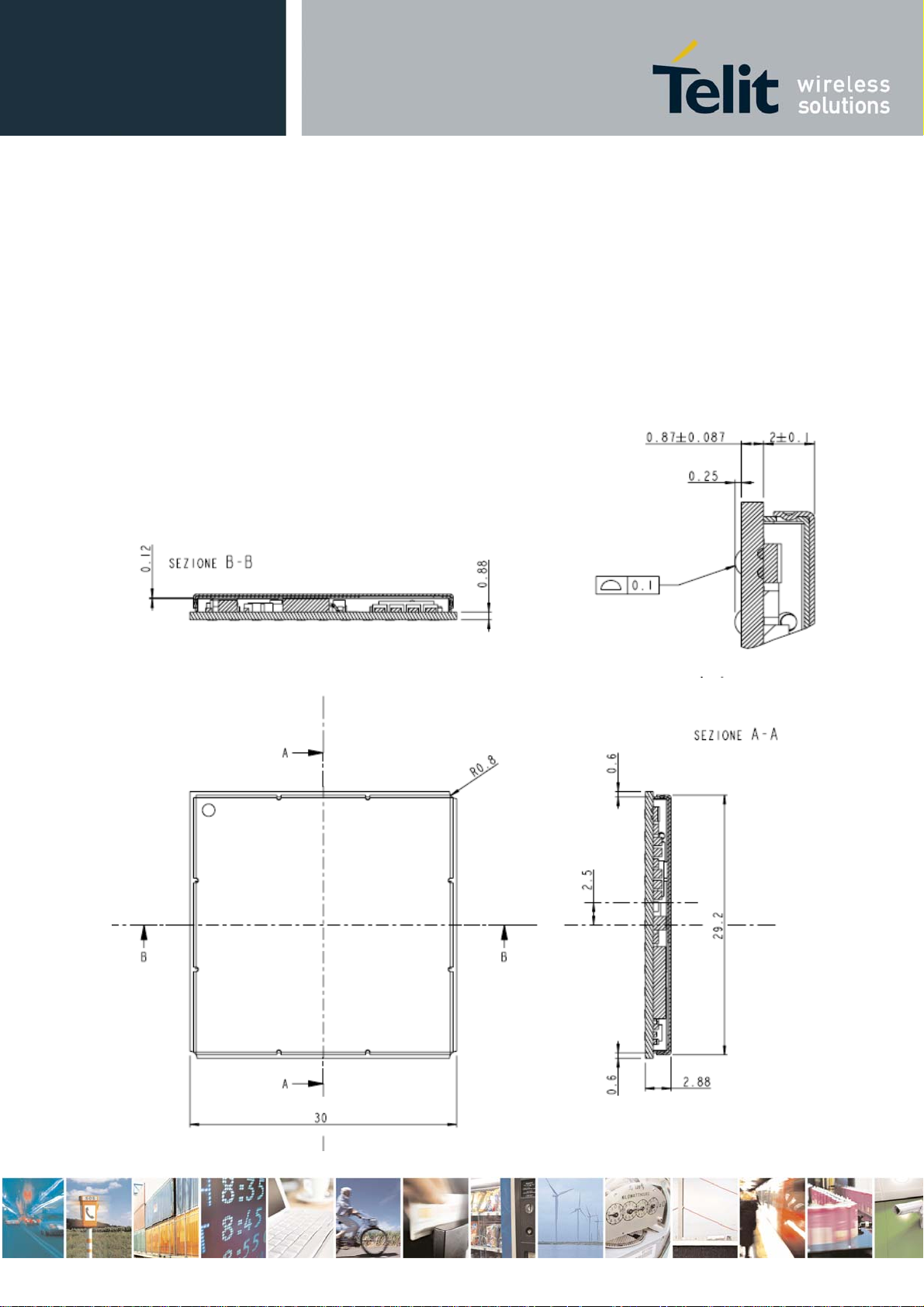
3. GE864-QUAD V2/GPS Mechanical Dimensions
3.1. GE864-QUAD V2/GPS
The Telit GE864-QUAD V2/GPS modules overall dimensions are:
Length: 30 mm
Width: 30 mm
Thickness : 2,9 mm
Weight: 4.2g
Reproduction forbidden without Telit Communications S.p.A. written authorization - All Rights Reserved. Page 12 of 94
Page 13
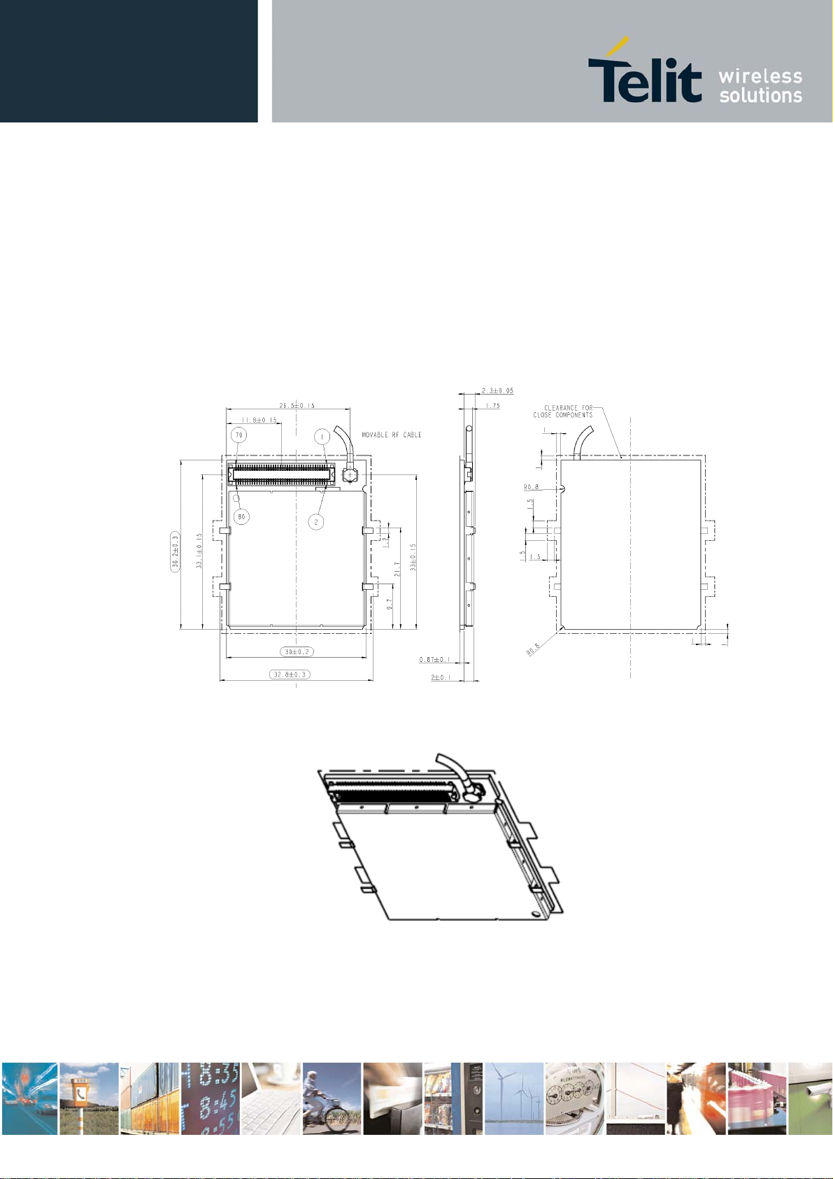
3.2. GC864-QUAD V2
The Telit GC864-QUAD V2 module overall dimensions are:
Length: 36.2 mm
Width: 30 mm
Thickness: 3.2 mm
Weight: 4.8g
GE/GC864-QUAD V2 and GE864-GPS Hardware User Guide
1vv0300915 Rev.5 – 2011-10-03
Reproduction forbidden without Telit Communications S.p.A. written authorization - All Rights Reserved. Page 13 of 94
Page 14
GE/GC864-QUAD V2 and GE864-GPS Hardware User Guide
1vv0300915 Rev.5 – 2011-10-03
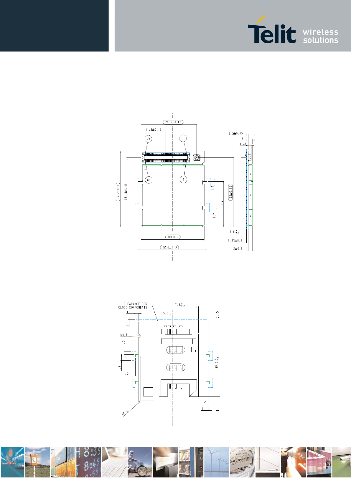
3.3. Mechanical View of Telit GC864-QUAD V2 with SIM
Holder
3.4. GC864-QUAD V2 Module Connections
Reproduction forbidden without Telit Communications S.p.A. written authorization - All Rights Reserved. Page 14 of 94
Page 15
GE/GC864-QUAD V2 and GE864-GPS Hardware User Guide
4. Electrical Connections
4.1. GE864-QUAD V2/GPS
4.1.1. PIN-OUT
The GE864-QUAD V2/GPS use 11x11 array BGA technology connection
1vv0300915 Rev.5 – 2011-10-03
Ball Signal I/O Function
Audio
F9
G8
G9
G10
J8
J9
J10
H9
H10
C10
C11
D4
D10
E9
D11
F10
AXE I Handsfree switching 100K CMOS 2.8V
MIC_HF+ AI Handsfree mic. input; phase +, nom. level 3mVrms Audio
MIC_MT- AI Handset mic.signal input; phase-, nom. level 50mVrms Audio
EAR_MT+ AO Handset earphone signal output, phase + Audio
MIC_MT+ AI Handset mic.signal input; phase+, nom. level 50mVrms Audio
MIC_HF- AI Handsfree mic.input; phase -, nom. level 3mVrms Audio
EAR_HF- AO Handsfree ear output, phase - Audio
EAR_MT- AO Handset earphone signal output, phase - Audio
EAR_HF+ AO Handsfree ear output, phase + Audio
SIM card interface
SIMCLK O External SIM signal – Clock 1,8 / 3V
SIMIN I External SIM signal - Presence (active low) Pull up 47K 1,8 / 3V
SIMVCC - External SIM signal – Power supply for the SIM 1,8 / 3V
SIMIO I/O External SIM signal - Data I/O Pull up 4.7K 1,8 / 3V
SIMRST O External SIM signal – Reset 1,8 / 3V
Auxiliary UART/Trace
TX_AUX O Auxiliary UART (TX Data to DTE) CMOS 2.8V
RX_AUX I Auxiliary UART (RX Data from DTE) CMOS 2.8V
Service pin shall be used to upgrade the module from
ASC1 (RX_TRACE, TX_TRACE). The pin shall be
H4
SERVICE I
tied low to enable the feature only in case of a SW
Update activity. It is required, for debug purpose, to
be connected
to a test pad on the final application.
Prog. / Data + HW Flow Control
B6
B7
D9
E7
E11
F7
F6
H8
C125/RING O Output for Ring indicator signal (RI) to DTE CMOS 2.8V
C108/DTR I Input for Data terminal ready signal (DTR) from DTE CMOS 2.8V
C109/DCD O Output for Data carrier detect signal (DCD) to DTE CMOS 2.8V
C103/TXD I Serial data input (TXD) from DTE CMOS 2.8V
C107/DSR O Output for Data set ready signal (DSR) to DTE CMOS 2.8V
C105/RTS I Input for Request to send signal (RTS) from DTE CMOS 2.8V
C106/CTS O Output for Clear to send signal (CTS) to DTE CMOS 2.8V
C104/RXD O Serial data output to DTE CMOS 2.8V
Internal
PULL UP
CMOS 2.8V
Type
Reproduction forbidden without Telit Communications S.p.A. written authorization - All Rights Reserved. Page 15 of 94
Page 16
GE/GC864-QUAD V2 and GE864-GPS Hardware User Guide
Ball Signal I/O Function
DAC and ADC
C7
J11
H11
A2
D8
E2
J5
L8
L4
D5
C1
E6
C2
B3
K8
B5
L9
K11
C9
H3
K7
D7
H5
A7
C8
E10
F8
G2
J4
A10
C6
G6
J1
K1
J2
K2
DAC_OUT AO Digital/Analog converter output D/A
ADC_IN1 AI Analog/Digital converter input A/D
ADC_IN2 AI Analog/Digital converter input A/D
Miscellaneous Functions
RESET# I Reset input
STAT_LED O Status indicator led CMOS 1.8V
VRTC AO VRTC Power
Input command for switching power ON or OFF (toggle
ON_OFF# I
command). The pulse to be sent to the GE864-QUAD V2
must be equal or greater than 1 second.
PWRMON O PWRMON CMOS 2.8V
GSM Antenna O Antenna output – 50 ohm RF
VAUX
(1)
AO Auxiliary 2.8V Output Power
Telit GPIO / DVI
GPIO_01 I/O GPIO_01 CMOS 2.8V
GPIO_02 / JDR I/O GPIO_02 / JDR CMOS 2.8V
GPIO_03 I/O GPIO_03 CMOS 2.8V
GPIO_04 /
TX_DISABLE
I/O GPIO_04 / TX_DISABLE CMOS 2.8V
GPIO_05 / RFTXMON I/O Telit GPIO05 Configurable GPIO / Transmitter ON monitor CMOS 2.8V
GPIO_06 / ALARM I/O Telit GPIO06 Configurable GPIO / ALARM CMOS 2.8V
GPIO_07 / BUZZER I/O Telit GPIO07 Configurable GPIO / Buzzer CMOS 2.8V
GPIO_08 I/O GPIO_08 CMOS 2.8V
GPIO_09 I/O GPIO_09 CMOS 2.8V
GPIO_10 / DVI_TX I/O GPIO_10 / DVI_TX- DVI audio
DVI_RX I/O DVI_RX - DVI audio
DVI_CLK I/O DVI_CLK - DVI audio
DVI_WA0 I/O DVI_WA0 - DVI audio
(1)
GPS_EXT_LNA_EN
GPS_PPS
GPS_RX
GPS_TX
(1)
(1)
(1)
GPS_WAKEUP
GPS_ON_OFF
GPS Antenna
(1)(2)
- -
(1)(2)
- -
(1)
(1)
(1)
O External LNA Enable CMOS 1.8V (GPS)
O Pulse Per Second CMOS 1.8V (GPS)
I Serial Data Input CMOS 2.8V (GPS)
O Serial Data Output CMOS 2.8V (GPS)
O Wake up output CMOS 2.8V (GPS)
I GPS Power Control CMOS 1.8V (GPS)
O Antenna output – 50 ohm RF
Diagnostic (to be connected to Vaux through a pull-up
resistor
Diagnostic (to be connected to ground
(2)(3)
(1)
CMOS 2.8V
(1)
CMOS 2.8V
(1)
CMOS 2.8V
(2)
GPS
(only for GE864-GPS)
)
Power Supply
VBATT - Main power supply Power
VBATT - Main power supply Power
VBATT - Main power supply Power
VBATT - Main power supply Power
1vv0300915 Rev.5 – 2011-10-03
Internal
PULL UP
Pull up 47K Pull up to VBATT
(1)
CMOS 2.8V
(2)(3)
)
Type
Reproduction forbidden without Telit Communications S.p.A. written authorization - All Rights Reserved. Page 16 of 94
Page 17

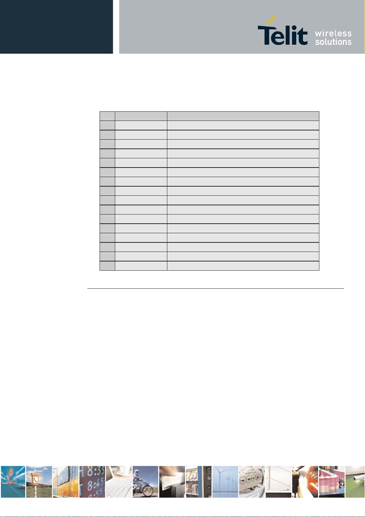
GE/GC864-QUAD V2 and GE864-GPS Hardware User Guide
Ball Signal I/O Function
A1
A11
D6
F1
F11
H1
H2
J3
K3
K4
K5
K6
L1
L2
L3
L6
L11
A8
B8
B9
B10
B11
A3
A4
A5
A6
A9
B1
B2
B4
C3
C4
C5
D1
D2
D3
E1
E3
E4
E5
E8
F2
GND - Ground Power
GND - Ground Power
GND - Ground Power
GND - Ground Power
GND - Ground Power
GND - Ground Power
GND - Ground Power
GND - Ground Power
GND - Ground Power
GND - Ground Power
GND - Ground Power
GND - Ground Power
GND - Ground Power
GND - Ground Power
GND - Ground Power
GND - Ground Power
GND - Ground Power
(2)
GND
(2)
GND
(2)
GND
(2)
GND
(2)
GND
- - Reserved
- - Reserved
- - Reserved
- - Reserved
- - Reserved
- - Reserved
- - Reserved
- - Reserved
- - Reserved
- - Reserved
- - Reserved
- - Reserved
- - Reserved
- - Reserved
- - Reserved
- - Reserved
- - Reserved
- - Reserved
- - Reserved
- - Reserved
-
-
-
-
-
Ground
Ground
Ground
Ground
Ground
(2)
(2)
(2)
(2)
(2)
RESERVED
1vv0300915 Rev.5 – 2011-10-03
Internal
PULL UP
Power
Power
Power
Power
Power
Type
Reproduction forbidden without Telit Communications S.p.A. written authorization - All Rights Reserved. Page 17 of 94
Page 18
GE/GC864-QUAD V2 and GE864-GPS Hardware User Guide
Ball Signal I/O Function
F3
F4
F5
G1
G3
G4
G5
G7
G11
H6
H7
J6
J7
K9
K10
L5
L7
L10
- - Reserved
- - Reserved
- - Reserved
- - Reserved
- - Reserved
- - Reserved
- - Reserved
- - Reserved
- - Reserved
- - Reserved
- - Reserved
- - Reserved
- - Reserved
- - Reserved
- - Reserved
- - Reserved
- - Reserved
- - Reserved
1vv0300915 Rev.5 – 2011-10-03
Internal
PULL UP
Type
(1) Ref. to Digital Voice Interface Application Note 80000NT10004a.
(2) Available only on GE864-GPS (in case of GE864-QUAD it has to be considered
RESERVED)
(3) Only for GE864-GPS: C6 ball (diagnostic) must be connected to VAUX (Ball D5)
through a pull up resistor (e.g. 47K) and G6 ball (diagnostic) must be connected to ground
(suggested through a 0 ohm resistor).
NOTE:
The GE864-QUAD V2/GPS Modules has one DVI port on the system.
NOTE:
Reserved pins must not be connected.
NOTE:
RTS must be connected to the GND (on the module side) if flow control is not used.
Reproduction forbidden without Telit Communications S.p.A. written authorization - All Rights Reserved. Page 18 of 94
Page 19
GE/GC864-QUAD V2 and GE864-GPS Hardware User Guide
1vv0300915 Rev.5 – 2011-10-03
NOTE:
If not used, pins must be left disconnected, with the exceptions listed in the table below:
J1, J2, K1, K2
(2)
A1, A8
(2)
B11
, D6, F1, F11, H1, H2, J3, K3,
K4, K5, K6, L1, L2, L3, L6, L11
E7
H8
F7
J5
A2
F10
D11
H4
B7
(2)
J4
(2)
G2
(2)
E10
(2)
F8
(2)
C6
(2)
G6
Ball Signal Function
VBATT Main power supply
(2)
(2)
, A11, B8
, B9
, B10
(2)
,
GND Ground
C103/TXD Serial data input (TXD) from DTE
C104/RXD Serial data output to DTE
C105/RTS Input for Request to send signal (RTS) from DTE
ON/OFF# Input command for switching power ON or OFF (toggle command).
RESET# Reset input
RX_TRACE RX Data for debug monitor
TX_TRACE TX Data for debug monitor
SERVICE SERVICE connection
DTR Input for Data terminal ready signal (DTR) from DTE
GPS_ON_OFF GPS Power Control
GPS_WAKEUP GPS Wake up output
GPS_RX GPS Serial data input
GPS_TX GPS Serial data output
- Diagnostic
- Diagnostic
(2) Available only on GE864-GPS (in case of GE864-QUAD V2 it has to be considered
RESERVED)
NOTE:
Only for GE864-GPS, do not leave the GPS_ON_OFF (ball J4) input pin floating. It’s
suggested to connect them to a pull-down (e.g.: 100k).
Reproduction forbidden without Telit Communications S.p.A. written authorization - All Rights Reserved. Page 19 of 94
Page 20
GE/GC864-QUAD V2 and GE864-GPS Hardware User Guide
1vv0300915 Rev.5 – 2011-10-03
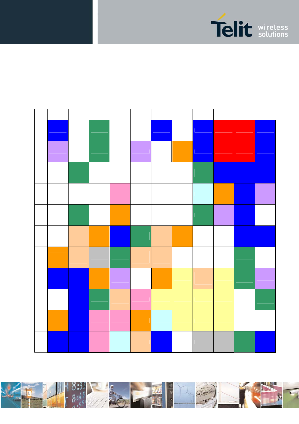
4.1.2. BGA Balls Layout
TOP VIEW
A B C D E F G H J K L
GND - GPIO_01 - - GND - GND VBATT VBATT GND
1
RESET* - GPIO_03 - VRTC -
2
GPIO_04 /
-
3
4
5
6
GPS_EXT_
7
LNA_EN3
8
GND1 GND1 GPS_PPS1
TX_DISAB
LE
-- - - SIMVCC - - - SERVICE
GPIO_06 /
-
ALARM
-
C125
RING
C108
DTR
/
/
- - - _ -
-
Diagnostic GND
DAC_OUT DVI_CLK
VAUX1
STAD_
LED
- - - DVI_WA0 ON_OFF* GND -
GPIO_02 /
JDR
C103
/
TXD
-
C106
/
CTS
C105
/
RTS
GPS_TX1
GPS_WAK
EUP1
Diagnostic - - GND GND
- -
MIC_HF+
GND VBATT VBATT GND
GPIO_10 /
DVI_TX
C104
/
RXD
GND GND GND
GPS_ON_
OFF1
- DVI_RX -
MIC_MT+
GND
GPIO_05 /
RFTXMON
PWRMON
GSM
Antenna
9
10
11
-
GPS
Antenna1
GND1 GND1
GND1
GND1
GPIO_09
SIMCLK SIMIO
SIMIN TX_AUX C107 / DSR GND - ADC_IN2 ADC_IN1 GPIO_08 GND
C109 /
DCD
SIMRST AXE MIC_MT- EAR_MT- MIC_HF- -
GPS_RX1
RX_AUX EAR_MT+ EAR_HF+ EAR_HF- - -
Reproduction forbidden without Telit Communications S.p.A. written authorization - All Rights Reserved. Page 20 of 94
GPIO_07 /
BUZZER
Page 21
GE/GC864-QUAD V2 and GE864-GPS Hardware User Guide
1vv0300915 Rev.5 – 2011-10-03
(1) Available only on GE864-GPS (in case of GE864-QUAD V2 it has to be considered RESERVED)
AUDIO Signals balls
SIM CARD interface balls
AUX UART&SERVICE Signals balls
Prog. / data + Hw Flow Control signals balls
ADC signals balls
MISCELLANEOUS functions signals balls
TELIT GPIO balls
GPS balls
POWER SUPPLY VBATT balls
POWER SUPPLY GND balls
RESERVED
Reproduction forbidden without Telit Communications S.p.A. written authorization - All Rights Reserved. Page 21 of 94
Page 22
GE/GC864-QUAD V2 and GE864-GPS Hardware User Guide
4.2. GC864-QUAD V2
4.2.1. PIN-OUT
The GC864-QUAD V2 uses an 80 pin Molex p.n. 53949-0878 male connector for the
connections with the external applications. This connector matches the 54150-0878 models.
Pin Signal I/O Function
Power Supply
1
2
3
4
5
6
7
8
9
10
11
12
13
14
15
16
181
19
20
21
22
VBATT - Main power supply Power
VBATT - Main power supply Power
VBATT - Main power supply Power
VBATT - Main power supply Power
GND - Ground Power
GND - Ground Power
GND - Ground Power
Audio
AXE I Handsfree switching
EAR_HF+ AO Handsfree ear output, phase + Audio
EAR_HF- AO Handsfree ear output, phase - Audio
EAR_MT+ AO Handset earphone signal output, phase + Audio
EAR_MT- AO Handset earphone signal output, phase - Audio
MIC_HF+ AI Handsfree microphone input; phase Audio
MIC_HF- AI Handsfree microphone input; phase Audio
MIC_MT+ AI Handset microphone signal input; phase+ Audio
MIC_MT- AI Handset microphone signal input; phase- Audio
SIM Card Interface
SIMVCC - External SIM signal – Power supply for the SIM 1.8 / 3V
SIMRST O External SIM signal – Reset 1.8 / 3V
SIMIO I/O External SIM signal - Data I/O 1.8 / 3V
SIMIN I External SIM signal - Presence (active low)
SIMCLK O External SIM signal – Clock 1.8 / 3V
1vv0300915 Rev.5 – 2011-10-03
Internal
Pull up
100K
47K
Type
CMOS 2.8V
1.8 / 3V
1
On this line a maximum of 10nF bypass capacitor is allowed
Reproduction forbidden without Telit Communications S.p.A. written authorization - All Rights Reserved. Page 22 of 94
Page 23

GE/GC864-QUAD V2 and GE864-GPS Hardware User Guide
Pin Signal I/O Function
Trace
23
24
47
25
26
27
28
29
30
31
32
37
38
39
40
45
46
49
53
54
55
36
59
63
65
66
67
68
70
71
73
RX_TRACE I RX Data for debug monitor CMOS 2.8V
TX_TRACE O TX Data for debug monitor CMOS 2.8V
Service pin shall be used to upgrade the module from ASC1 (RX_TRACE,
SERVICE I
C103/TXD I Serial data input (TXD) from DTE CMOS 2.8V
C104/RXD O Serial data output (RXD) to DTE CMOS 2.8V
C107/DSR O Output for Data set ready signal (DSR) to DTE CMOS 2.8V
C106/CTS O Output for Clear to send signal (CTS) to DTE CMOS 2.8V
C108/DTR I Input for Data terminal ready signal (DTR) from DTE CMOS 2.8V
C125/RING O Output for Ring indicator signal (RI) to DTE CMOS 2.8V
C105/RTS I Input for Request to send signal (RTS) from DTE CMOS 2.8V
C109/DCD O Output for Data carrier detect signal (DCD) to DTE CMOS 2.8V
ADC_IN1 AI Analog/Digital converter input A/D
ADC_IN2 AI Analog/Digital converter input A/D
ADC_IN3 AI Analog/Digital converter input A/D
DAC_OUT AO Digital/Analog converter output D/A
STAT_LED O Status indicator led CMOS 1.8V
GND - Ground Ground
PWRMON O Power ON Monitor CMOS 2.8V
ON/OFF* I
RESET* I Reset input
VRTC AO VRTC Backup capacitor Power
DVI_CLK - DVI_CLK (Digital Voice Interface Clock) CMOS 2.8V
TGPIO_04/TXCNTRL I/O Telit GPIO4 Configurable GPIO / RF Transmission Control CMOS 2.8V
TGPIO_10/DVI_TX I/O Telit GPIO10 Configurable GPIO / DVI_TX (Digital Voice Interface) CMOS 2.8V
DVI_RX I/O DVI_RX (Digital Voice Interface) CMOS 2.8V
TGPIO_03 I/O Telit GPIO3 Configurable GPIO CMOS 2.8V
TGPIO_08 I/O Telit GPIO8 Configurable GPIO CMOS 2.8V
TGPIO_06 / ALARM I/O Telit GPIO6 Configurable GPIO / ALARM CMOS 2.8V
TGPIO_01 I/O Telit GPIO1 Configurable GPIO CMOS 2.8V
DVI_WAO I/O DVI_WAO (Digital Voice Interface) CMOS 2.8V
TGPIO_07 / BUZZER I/O Telit GPIO7 Configurable GPIO / Buzzer CMOS 2.8V
TX_TRACE). The pin shall be tied low to enable the feature only in case of a
SW Update activity. It is required, for debug purpose, to be connected
to a test pad on the final application.
Prog. / Data + Hw Flow Control
DAC and ADC
Miscellaneous Functions
Input command for switching power ON or OFF (toggle command). The
pulse to be sent to the GC864-QUAD V2 must be equal or greater than 1
second.
Telit GPIO / DVI
1vv0300915 Rev.5 – 2011-10-03
Internal
Pull up
2.2K
47K
Type
CMOS 2.8V
Pull up to VBATT
Reproduction forbidden without Telit Communications S.p.A. written authorization - All Rights Reserved. Page 23 of 94
Page 24
GE/GC864-QUAD V2 and GE864-GPS Hardware User Guide
Pin Signal I/O Function
74
76
78
17
33
34
35
41
42
43
44
48
50
51
52
56
57
58
60
61
62
64
69
72
75
77
79
80
TGPIO_02 / JDR I/O Telit GPIO02 I/O pin / Jammer detect report CMOS 2.8V
TGPIO_09 I/O Telit GPIO9 Configurable GPIO CMOS 2.8V
TGPIO_05/
RFTXMON
Reserved -
Reserved -
Reserved -
Reserved -
Reserved -
Reserved -
Reserved -
Reserved -
Reserved
Reserved -
Reserved
Reserved
Reserved
Reserved
Reserved
Reserved
Reserved
Reserved
Reserved
Reserved -
Reserved
Reserved
Reserved
Reserved -
Reserved -
I/O Telit GPIO05 Configurable GPIO / Transmitter ON monitor CMOS 2.8V
RESERVED
-
-
-
-
-
-
-
-
-
-
-
-
-
1vv0300915 Rev.5 – 2011-10-03
Internal
Pull up
Type
NOTE:
The GC864-QUAD V2 Modules has one DVI ports on the system interface.
NOTE:
Reserved pins must not be connected.
NOTE:
RTS must be connected to the GND (on the module side) if flow control is not used.
Reproduction forbidden without Telit Communications S.p.A. written authorization - All Rights Reserved. Page 24 of 94
Page 25
GE/GC864-QUAD V2 and GE864-GPS Hardware User Guide
1vv0300915 Rev.5 – 2011-10-03
NOTE:
If not used, almost all pins must be left disconnected. The only exceptions are the following
pins:
Pin Signal Function
VBATT Main power supply
1
VBATT Main power supply
2
VBATT Main power supply
3
VBATT Main power supply
4
GND Ground
5
GND Ground
6
GND Ground
7
GND Ground
46
C103/TXD Serial data input (TXD) from DTE
25
C104/RXD Serial data output to DTE
26
C105/RTS Input for Request to send signal (RTS) from DTE
31
ON/OFF* Input command for switching power ON or OFF (toggle command).
53
RESET* Reset input
54
RX_TRACE RX Data for debug monitor
23
TX_TRACE TX Data for debug monitor
24
SERVICE SERVICE connection
47
4.2.2. GC864-QUAD V2 Antenna Connector
The GC864-QUAD V2 module is equipped with a 50 ohm RF connector from Murata, GSC
type P/N MM9329-2700B.
The counterpart suitable is Murata MXTK92 Type or MXTK88 Type.
Moreover, the GC864-QUAD V2 has the antenna pads on the back side of the PCB. This
allows the manual soldering of the coaxial cable directly on the back side of the PCB.
However, the soldering is not an advisable solution for a reliable connection of the antenna.
Reproduction forbidden without Telit Communications S.p.A. written authorization - All Rights Reserved. Page 25 of 94
Page 26
GE/GC864-QUAD V2 and GE864-GPS Hardware User Guide
1vv0300915 Rev.5 – 2011-10-03
5. Hardware Commands
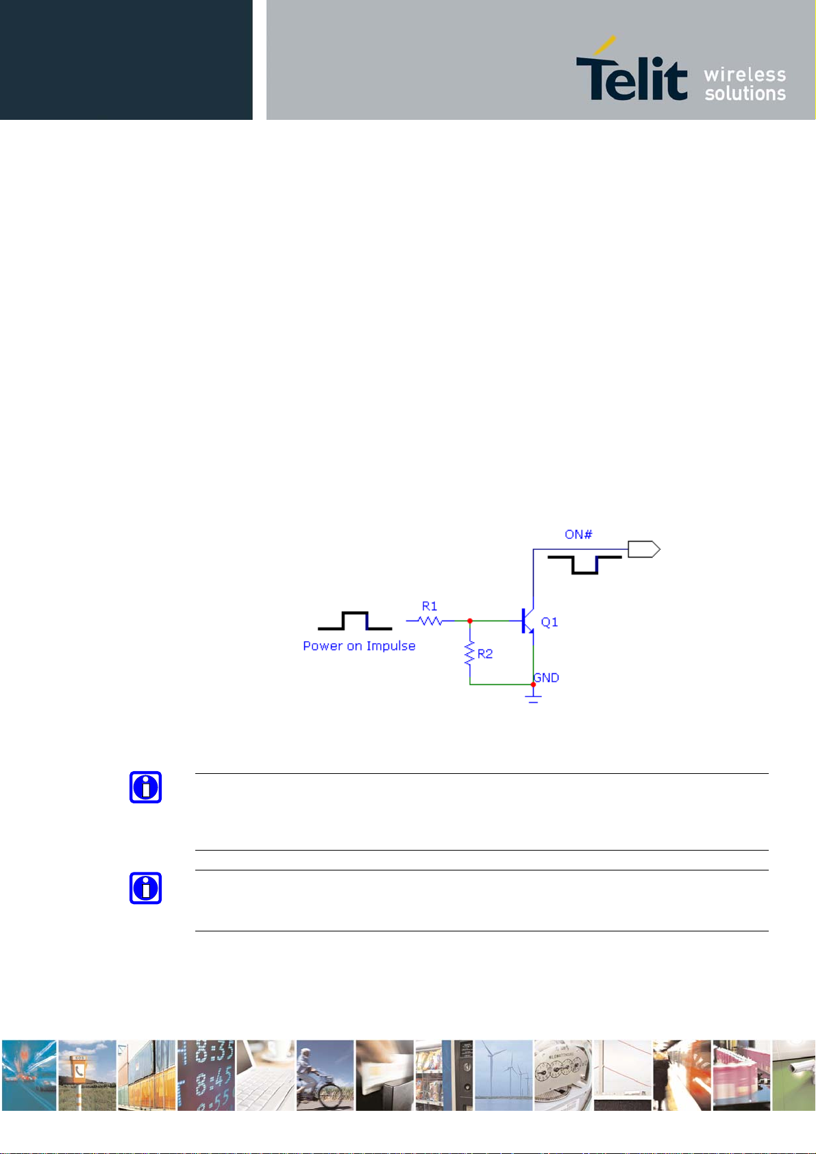
5.1. Turning ON the GE/GC864-QUAD V2 and GE864-GPS
To turn ON the GE/GC864-QUAD V2 AND GE864-GPS the pad ON# must be tied low for
at least 1 second and then released. Pulse duration less than 1000ms should also start the
power on procedure, but this is not guaranteed.
When the power supply voltage is lower than 3.4V the pad ON# must be tied low for at least
5 seconds.
The maximum current that can be drained from the ON# pad is 0.1 mA.
A simple circuit to do it is:
NOTE:
Don't use any pull up resistor on the ON# line, it is internally pulled up. Using pull up resistor
may bring to latch up problems on the module, power regulator and improper power on/off of
the module. The line ON# must be connected only in open collector configuration.
NOTE:
In this document all the lines that are inverted, hence have active low signals are labeled with
a name that ends with a "#".
Reproduction forbidden without Telit Communications S.p.A. written authorization - All Rights Reserved. Page 26 of 94
Page 27
GE/GC864-QUAD V2 and GE864-GPS Hardware User Guide
1vv0300915 Rev.5 – 2011-10-03
TIP:
To check if the device has powered on, the hardware line PWRMON should be monitored.
After 1000ms the line raised up the device could be considered powered on.
NOTE:
When the power supply voltage is lower than 3.4V, to turn ON the module, the pad ON# must
be tied low for at least 3 seconds.
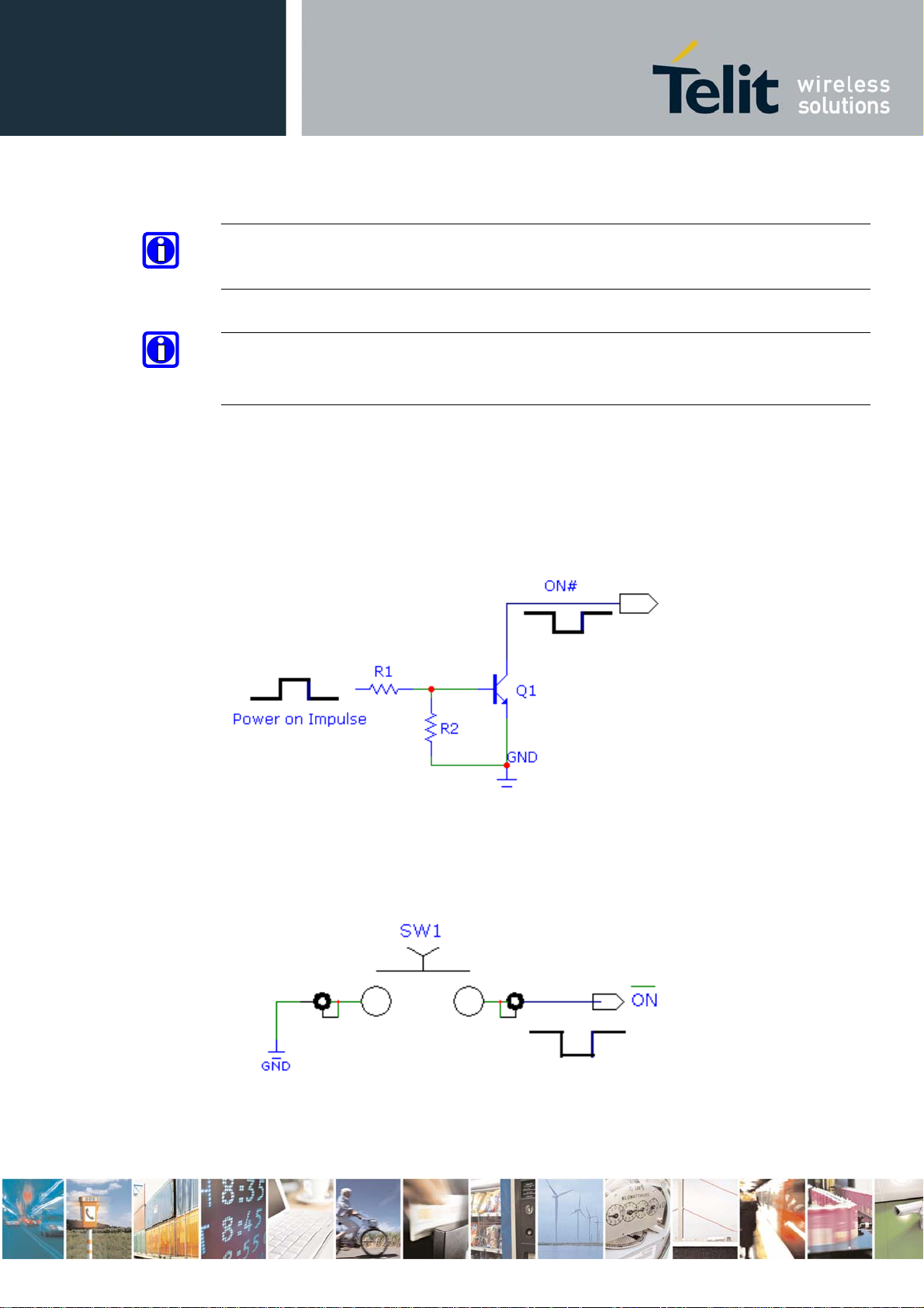
For example:
1- Let us assume you need to drive the ON# pad with a totem pole output from +1.8V up to
5V microcontroller:
2- Let us assume you need to drive the ON# pad directly with an ON/OFF button:
Reproduction forbidden without Telit Communications S.p.A. written authorization - All Rights Reserved. Page 27 of 94
Page 28
GE/GC864-QUAD V2 and GE864-GPS Hardware User Guide
1vv0300915 Rev.5 – 2011-10-03
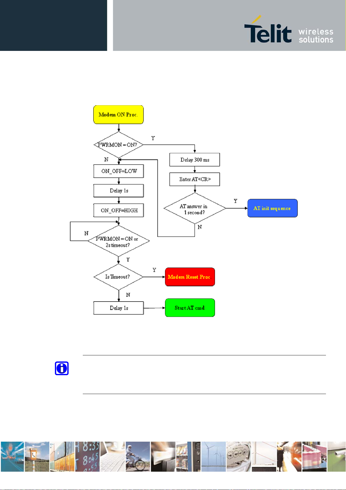
A flow chart showing the proper turn on procedure is displayed below:
NOTE:
In order to avoid a back powering effect it is recommended to avoid having any HIGH logic
level signal applied to the digital pins of the module when is powered OFF or during an
ON/OFF transition.
Reproduction forbidden without Telit Communications S.p.A. written authorization - All Rights Reserved. Page 28 of 94
Page 29
GE/GC864-QUAD V2 and GE864-GPS Hardware User Guide
1vv0300915 Rev.5 – 2011-10-03
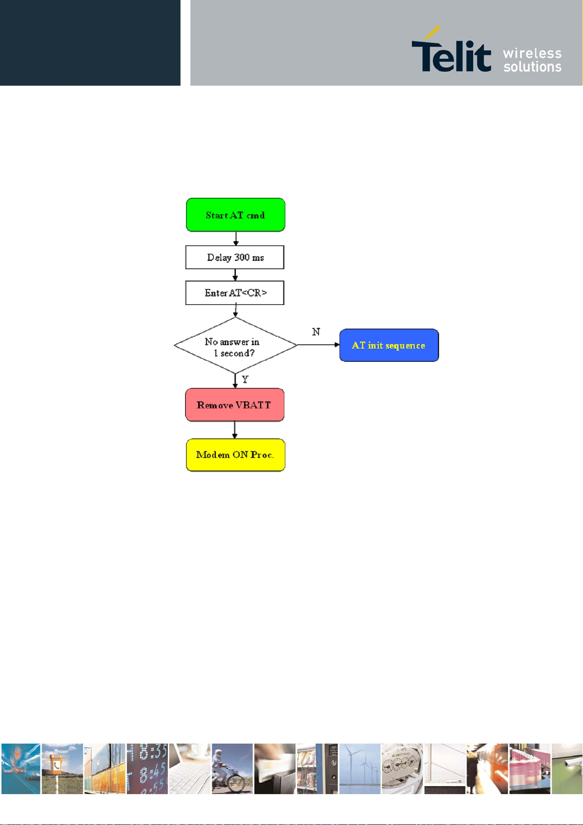
A flow chart showing the AT commands managing procedure is displayed below:
Reproduction forbidden without Telit Communications S.p.A. written authorization - All Rights Reserved. Page 29 of 94
Page 30

GE/GC864-QUAD V2 and GE864-GPS Hardware User Guide
1vv0300915 Rev.5 – 2011-10-03
5.2. Turning OFF the GE/GC864-QUAD V2 and GE864 GPS
The turning off of the device can be done in two ways:
via AT command (see Software User Guide AT#SHDN)
by tying low pin ON#
Either ways, when the device issues a detach request to the network informing that the device
will not be reachable any more.
To turn OFF the module the pad ON# must be tied low for at least 2 seconds and then
released.
The same circuitry and timing for the power on shall be used.
The device shuts down after the release of the ON# pad.
The following flow chart shows the proper turnoff procedure:
Reproduction forbidden without Telit Communications S.p.A. written authorization - All Rights Reserved. Page 30 of 94
Page 31

GE/GC864-QUAD V2 and GE864-GPS Hardware User Guide
1vv0300915 Rev.5 – 2011-10-03
TIP:
To check if the device has been powered off, the hardware line PWRMON must be
monitored. The device is powered off when PWRMON goes low.
NOTE:
In order to avoid a back powering effect it is recommended to avoid having any HIGH logic
level signal applied to the digital pins of the module when is powered OFF or during an
ON/OFF transition.
Reproduction forbidden without Telit Communications S.p.A. written authorization - All Rights Reserved. Page 31 of 94
Page 32

GE/GC864-QUAD V2 and GE864-GPS Hardware User Guide
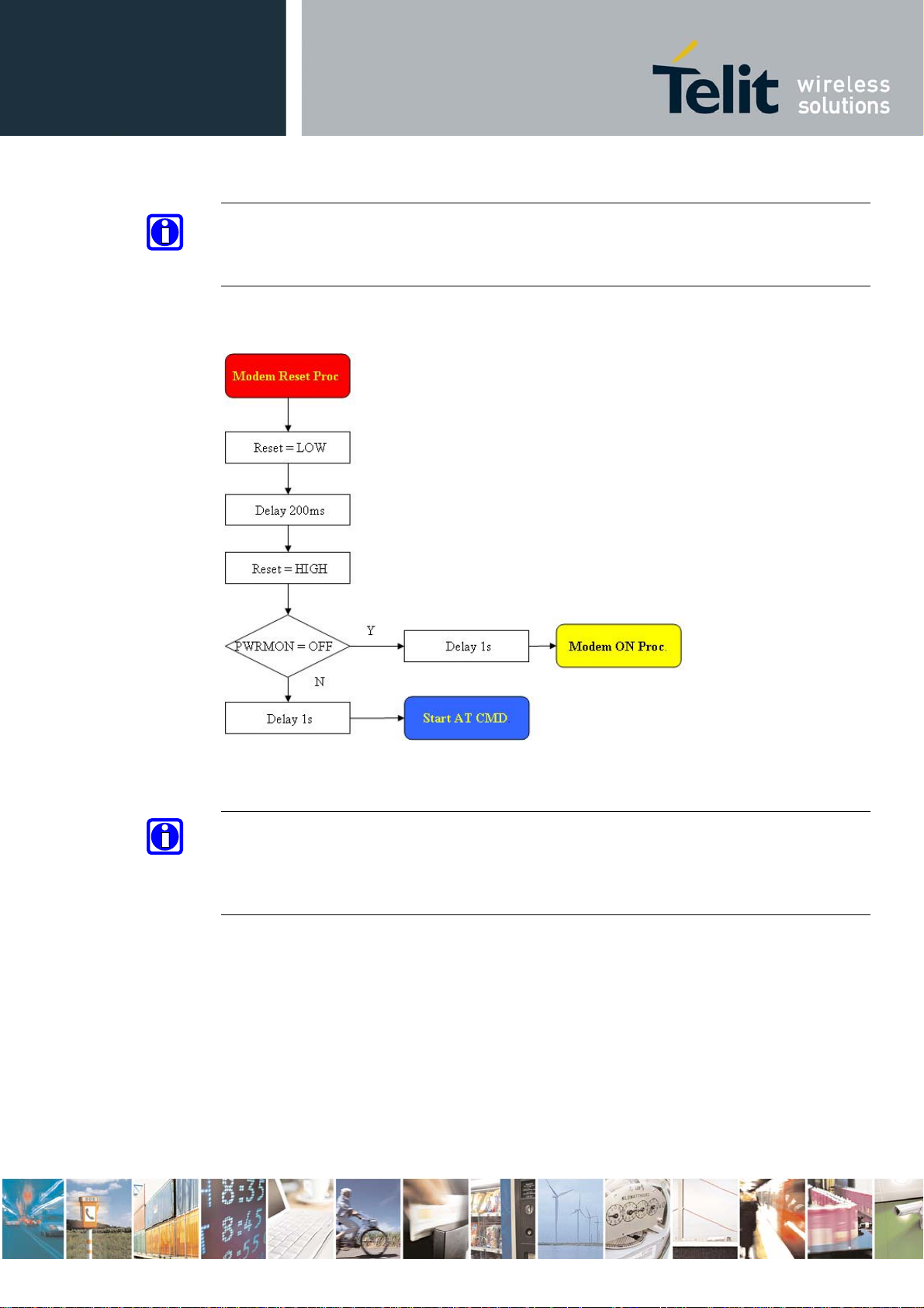
5.3. Hardware Unconditional Restart
WARNING:
The hardware unconditional Restart must not be used during normal operation of the device
since it does not detach the device from the network. It shall be kept as an emergency exit
procedure to be done in the rare case that the device gets stacked waiting for some network or
SIM responses.
To unconditionally restart the module, the pad RESET# must be tied low for at least 200
milliseconds and then released.
The maximum current that can be drained from the RESET# pad is 0.15 mA.
A simple circuit to do it is:
1vv0300915 Rev.5 – 2011-10-03
NOTE:
Do not use any pull up resistor on the RESET# line or any totem pole digital output. Using
pull up resistor may bring to latch up problems on the module power regulator and improper
functioning of the module. The line RESET# must be connected only in open collector
configuration.
Reproduction forbidden without Telit Communications S.p.A. written authorization - All Rights Reserved. Page 32 of 94
Page 33
GE/GC864-QUAD V2 and GE864-GPS Hardware User Guide
1vv0300915 Rev.5 – 2011-10-03
TIP:
The unconditional hardware Restart must always be implemented on the boards and must be
used by the software as an emergency exit procedure.
The following flow chart shows the proper RESET procedure:
NOTE:
In order to avoid a back powering effect it is recommended to avoid having any HIGH logic
level signal applied to the digital pins of the module when is powered OFF or during an
ON/OFF transition.
Reproduction forbidden without Telit Communications S.p.A. written authorization - All Rights Reserved. Page 33 of 94
Page 34

GE/GC864-QUAD V2 and GE864-GPS Hardware User Guide
1vv0300915 Rev.5 – 2011-10-03
For example:
Let us assume you need to drive the RESET# pad with a totem pole output from +1.8V up to
5V microcontroller
This signal is internally pulled up so the pin can be left floating if not used.
Reproduction forbidden without Telit Communications S.p.A. written authorization - All Rights Reserved. Page 34 of 94
Page 35

GE/GC864-QUAD V2 and GE864-GPS Hardware User Guide
1vv0300915 Rev.5 – 2011-10-03
5.4. Turning ON/OFF the GPS (only GE864-GPS)
When GPS is not in GSM controlled mode (controlled by GSM) a specific sequence to
power-up and shutdown it’s needed.
5.4.1. GPS Power-up
After you first apply power the GPS part of GE864-GPS goes into a low-power mode status.
To switch ON the GPS part is requested a pulse at the input pin GPS_ON_OFF. In order to
know when the GPS is ready to accept the pulse, the application in the host controller can
either:
- Wait for a fixed interval
- Monitor a pulse on GPS_WAKEUP output
- Assert a pulse on the GPS_ON_OFF input every seconds until GPS starts indicating a
high on GPS_WAKEUP output or generation of serial messages.
The GPS starts after asserting a rising edge pulse on GPS_ON_OFF input and when high
level persists for at least three cycles of RTC clock. Before asserting another pulse to
GPS_ON_OFF input, the host controller must put it at low state and hold it low for at least
three cycles of the RTC clock.
The GPS_WAKEUP output goes high indicating the GPS is working.
As suggested in chapter 4.1.1 (Pin Out) do not leave the GPS_ON_OFF (ball J4) input pin
floating. It’ suggested to connect it to a pull-down resistor (e.g.: 100k)
5.4.2. GPS Shutdown
When GPS is working, a pulse on the GPS_ON_OFF input origins the GPS shutdown
sequence.
As explained for power-up, a rising edge pulse followed by an high level logic for at least
three cycles of RTC clock is recognized as an GPS_ON_OFF pulse. Before asserting
another pulse to GPS_ON_OFF input, the host controller must put it at low state and hold it
low for at least three cycles of the RTC clock.
The shutdown sequence may take anywhere from 10ms to 900ms, depending on operation in
progress.
Avoid any abrupt, uncontrolled removal of power (VBATT) while GPS is operating. Before
removing the supply from the module, perform the shutdown sequence. Performance
degradation may be the consequences of any uncontrolled removal of main power.
Reproduction forbidden without Telit Communications S.p.A. written authorization - All Rights Reserved. Page 35 of 94
Page 36

GE/GC864-QUAD V2 and GE864-GPS Hardware User Guide
6. Power Supply
The power supply circuitry and board layout are a fundamental part of the product design and
they strongly reflect on the product overall performances, hence read carefully the following
requirements and guidelines for a proper design.
6.1. Power Supply Requirements
Condition Value
Nominal Supply Voltage 3.80 V
Normal operating Voltage Range 3.40 V - 4.20 V
Extended operating Voltage Range 3.22 V – 4.50 V
TIP:
The supply voltage is directly measured between VBATT and GND balls. It must stay within
the Wide Supply Voltage tolerant range including any drop voltage and overshoot voltage
(during the slot TX, for example).
NOTE:
The Operating Voltage Range MUST never be exceeded also in power off condition; care
must be taken in order to fulfill min/max voltage requirement
1vv0300915 Rev.5 – 2011-10-03
NOTE:
When the power supply voltage is lower than 3.4V, to turn ON the module, the pad ON# must
be tied low for at least 3 seconds
Reproduction forbidden without Telit Communications S.p.A. written authorization - All Rights Reserved. Page 36 of 94
Page 37

GE/GC864-QUAD V2 and GE864-GPS Hardware User Guide
6.2. Power Consumption
The table below shows the power consumption of the GSM/GPRS section in different
working modes (common for all the modules):
1vv0300915 Rev.5 – 2011-10-03
Switched Off <62 uA
Mode
T
h
SWITCHED OFF
e
G
AT+CFUN=1 16.0 Normal mode: full functionality of the module
S
AT+CFUN=4 16.0
M
AT+CFUN=0 or =5
s
y
s
CSD TX and RX mode
t
e
DCS1800 CSD PL0 175
m
GPRS (class 10) 1TX
i
DCS1800 PL0 160
s
GPRS (class 10) 2TX
m
DCS1800 PL0 290
a
GE\GC864-QUAD V2 and GE864-GPS (GPS OFF)
Average
(mA)
Module supplied but Switched Off
IDLE mode
Disabled TX and RX; module is not registered on the
network
3.9 Paging Multiframe 2
2.5 Paging Multiframe 3
2.4 Paging Multiframe 4
1.5 Paging Multiframe 9
GSM VOICE CALL GSM900 CSD PL5 240
GPRS Sending data mode GSM900 PL5 225
GPRS Sending data mode GSM900 PL5 420
Mode description
For the GE864-GPS, the additional current consumption of the GPS section in different
operating modes is:
GE864-GPS (GPS ON)
-
Mode Average (mA) Mode description
HIBERNATE
Acquisition mode
Tracking mode
Additional current -
<0.045 only RTC and RAM supplied
45
37
Reproduction forbidden without Telit Communications S.p.A. written authorization - All Rights Reserved. Page 37 of 94
Page 38

GE/GC864-QUAD V2 and GE864-GPS Hardware User Guide
1vv0300915 Rev.5 – 2011-10-03
The GSM system is made in a way that the RF transmission is not continuous, else it is
packed into bursts at a base frequency of about 216 Hz, the relative current peaks can be as
high as about 2A. Therefore the power supply has to be designed in order to withstand with
these current peaks without big voltage drops; this means that both the electrical design and
the board layout must be designed for this current flow.
If the layout of the PCB is not well designed a strong noise floor is generated on the ground
and the supply; this will reflect on all the audio paths producing an audible annoying noise at
216 Hz; if the voltage drop during the peak current absorption is too much, then the device
may even shutdown as a consequence of the supply voltage drop.
TIP:
The electrical design for the Power supply should be made ensuring it will be capable of a
peak current output of at least 2A.
6.3. General Design Rules
The principal guidelines for the Power Supply Design embrace three different design steps:
the electrical design
the thermal design
the PCB layout.
6.3.1. Electrical Design Guidelines
The electrical design of the power supply depends strongly from the power source where this
power is drained. We will distinguish them into three categories:
+5V input (typically PC internal regulator output)
+12V input (typically automotive)
Battery
6.3.1.1. +5V input Source Power Supply Design Guidelines
The desired output for the power supply is 3.8V, hence there is no big difference
between the input source and the desired output. A linear regulator can be used. A
switching power supply will not be suited because of the low drop out
requirements.
When using a linear regulator, a proper heat sink shall be provided in order to
dissipate the power generated.
A Bypass low ESR capacitor of adequate capacity must be provided in order to
cut the current absorption peaks close to the module, a 100F tantalum capacitor
is usually suited.
Reproduction forbidden without Telit Communications S.p.A. written authorization - All Rights Reserved. Page 38 of 94
Page 39

GE/GC864-QUAD V2 and GE864-GPS Hardware User Guide
1vv0300915 Rev.5 – 2011-10-03
Make sure the low ESR capacitor on the power supply output (usually a tantalum
one) is rated at least 10V.
A protection diode can be inserted close to the power input, in order to save the
module from power polarity inversion.
An example of linear regulator with 5V input is:
6.3.1.2. +12V input Source Power Supply Design Guidelines
The desired output for the power supply is 3.8V, hence, due to the big difference
between the input source and the desired output, a linear regulator is not suited
and shall not be used. A switching power supply will be preferable because of its
better efficiency especially with the 2A peak current load represented by the
module.
When using a switching regulator, a 500kHz (or more) switching frequency
regulator is preferable, because of its smaller inductor size and its faster transient
response. This allows the regulator to respond quickly to the current peaks
absorption.
In any case the frequency and switching design selection is related to the
application to be developed, due to the fact that the switching frequency could
also generate EMC interferences.
Reproduction forbidden without Telit Communications S.p.A. written authorization - All Rights Reserved. Page 39 of 94
Page 40

GE/GC864-QUAD V2 and GE864-GPS Hardware User Guide
1vv0300915 Rev.5 – 2011-10-03
As far as car PB battery, the input voltage can rise up to 15.8V. This must be kept
in mind when choosing components: all components in the power supply must
withstand this voltage.
A Bypass low ESR capacitor of adequate capacity must be provided, in order to
cut the current absorption peaks. A 100F tantalum capacitor is typically used.
Make sure the low ESR capacitor on the power supply output (usually a tantalum
one) is rated at least 10V.
As far as car applications, a spike protection diode must be inserted close to the
power input, in order to clean the supply from spikes.
A protection diode can be inserted close to the power input, in order to save the
module from power polarity inversion. This can be the same diode used for spike
protection.
An example of switching regulator with 12V input is in the schematic below (split in 2 parts):
Reproduction forbidden without Telit Communications S.p.A. written authorization - All Rights Reserved. Page 40 of 94
Page 41

GE/GC864-QUAD V2 and GE864-GPS Hardware User Guide
1vv0300915 Rev.5 – 2011-10-03
6.3.1.3. Battery Source Power Supply Design Guidelines
The desired nominal output for the power supply is 3.8V and the maximum voltage
allowed is 4.2V, hence a single 3.7V Li-Ion cell battery type is suited for supplying the
power to the Telit GE/GC864-QUAD V2 AND GE864-GPSmodules.
The three cells Ni/Cd or Ni/MH 3,6 V Nom. battery types or 4V PB types MUST NOT
BE USED DIRECTLY since their maximum voltage can rise over the absolute
maximum voltage for the module and damage it.
WARNING:
DON'T USE any Ni-Cd, Ni-MH, and Pb battery types directly connected with GE/GC864QUAD V2 and GE864-GPS. Their use can lead to overvoltage on the module and damage it.
USE ONLY Li-Ion battery types.
A Bypass low ESR capacitor of adequate capacity must be provided in order to cut
the current absorption peaks, a 100F tantalum capacitor is usually suited.
Make sure the low ESR capacitor (usually a tantalum one) is rated at least 10V.
A protection diode should be inserted close to the power input, in order to save the
module from power polarity inversion. Otherwise the battery connector should be
done in a way to avoid polarity inversions when connecting the battery.
The battery capacity must be at least 500mAh in order to withstand the current peaks
of 2A; the suggested capacity is from 500mAh to 1000mAh.
Reproduction forbidden without Telit Communications S.p.A. written authorization - All Rights Reserved. Page 41 of 94
Page 42

GE/GC864-QUAD V2 and GE864-GPS Hardware User Guide
6.3.2. Thermal Design Guidelines
The thermal design for the power supply heat sink must be done with the following
specifications:
Average current consumption during transmission @PWR level max: 500mA
Average current consumption during transmission @ PWR level min: 100mA
Average current during Power Saving (CFUN=5): from 1.5 to 3.9mA
Average current during idle (Power Saving disabled): 16mA
NOTE:
The average consumption during transmissions depends on the power level at which the
device is requested to transmit by the network. The average current consumption hence varies
significantly.
1vv0300915 Rev.5 – 2011-10-03
Considering the very low current during idle, especially if Power Saving function is enabled,
it is possible to consider from the thermal point of view that the device absorbs current
significantly only during calls.
If we assume that the device stays into transmission for short periods of time (let us say few
minutes) and then remains for a quite long time in idle (let us say one hour), then the power
supply has always the time to cool down between the calls, and the heat sink could be smaller
than the calculated one for 500mA maximum RMS current, or even could be the simple chip
package (no heat sink).
Moreover, in the average network conditions, the device is requested to transmit at a lower
power level than the maximum, hence the current consumption will be less than 500mA,
usually around 150mA.
For these reasons the thermal design is rarely a concern and the simple ground plane where
the power supply chip is placed grants a good thermal condition to avoid overheating as well.
As far as the heat generated by GC/GE864-QUAD V2 and GE864-GPS , you can consider it
to be during transmissions of 1W max during CSD/VOICE calls and 2W max during class10
GPRS upload.
This generated heat will be mostly conducted to the ground plane under GC/GE864-QUAD
V2 AND GE864-GPS ; you must ensure that your application can dissipate it.
Reproduction forbidden without Telit Communications S.p.A. written authorization - All Rights Reserved. Page 42 of 94
Page 43

GE/GC864-QUAD V2 and GE864-GPS Hardware User Guide
6.3.3. Power Supply PCB Layout Guidelines
As seen on the electrical design guidelines the power supply shall have a low ESR capacitor
on the output to cut the current peaks and a protection diode on the input to protect the supply
from spikes and polarity inversion. The placement of these components is crucial for the
correct working of the circuitry. A misplaced component can be useless or can even decrease
the power supply performances.
The Bypass low ESR capacitor must be placed close to the Telit GE/GC864-QUAD V2
and GE864-GPS power input pads or in the case the power supply is a switching type it
can be placed close to the inductor to cut the ripple provided the PCB trace from the
capacitor to the GE/GC864-QUAD V2 and GE864-GPS wide enough to ensure a dropless
connection even during the 2A current peaks.
The protection diode must be placed close to the input connector where the power source is
drained.
1vv0300915 Rev.5 – 2011-10-03
The PCB traces from the input connector to the power regulator IC must be wide enough to
ensure no voltage drops occur when the 2A current peaks are absorbed. Note that this is not
made in order to save power loss but especially to avoid the voltage drops on the power
line at the current peaks frequency of 216 Hz that will reflect on all the components
connected to that supply, introducing the noise floor at the burst base frequency. For this
reason while a voltage drop of 300-400 mV may be acceptable from the power loss point
of view, the same voltage drop may not be acceptable from the noise point of view. If your
application does not have audio interface but only uses the data feature of the Telit
GE/GC864-QUAD V2 and GE864-GPSthen this noise is not so disturbing and power
supply layout design can be more forgiving.
The PCB traces to the GE/GC864-QUAD V2 and GE864-GPS and the Bypass capacitor
must be wide enough to ensure no significant voltage drops occur when the 2A current
peaks are absorbed. This is for the same reason as previous point. Try to keep this trace as
short as possible.
The PCB traces connecting the Switching output to the inductor and the switching diode
must be kept as short as possible by placing the inductor and the diode very close to the
power switching IC (only for switching power supply). This is done in order to reduce the
radiated field (noise) at the switching frequency (100-500 kHz usually).
The use of a good common ground plane is suggested.
The placement of the power supply on the board must be done in such a way to guarantee
that the high current return paths in the ground plane are not overlapped to any noise
sensitive circuitry as the microphone amplifier/buffer or earphone amplifier.
The power supply input cables must be kept separate from noise sensitive lines such as
microphone/earphone cables.
Reproduction forbidden without Telit Communications S.p.A. written authorization - All Rights Reserved. Page 43 of 94
Page 44

GE/GC864-QUAD V2 and GE864-GPS Hardware User Guide
6.3.4. Parameters for ATEX Applications
In order to integrate the Telit’s modules into an ATEX application, the appropriate reference
standard IEC EN xx and integrations shall be followed.
Below are listed parameters and useful information to integrate the module in your
application:
GE864-QUAD V2
Total capacity: 27.45 uF
Total inductance: 55.20 nH
No voltage upper than supply voltage is present in the module.
1vv0300915 Rev.5 – 2011-10-03
No step-up converters are present in the module.
GC864-QUAD V2
Total capacity: 27.45 uF
Total inductance: 55.20 nH
No voltage upper than supply voltage is present in the module.
No step-up converters are present in the module.
GE864-GPS
Total capacity: 33.26 uF
Total inductance: 233 nH
No voltage upper than supply voltage is present in the module.
No step-up converters are present in the module.
Reproduction forbidden without Telit Communications S.p.A. written authorization - All Rights Reserved. Page 44 of 94
Page 45

GE/GC864-QUAD V2 and GE864-GPS Hardware User Guide
1vv0300915 Rev.5 – 2011-10-03
7. Antenna
The antenna(s) connection and board layout design are the most important part in the full
product design and they strongly reflect on the product overall performances, hence read
carefully and follow the requirements and the guidelines for a proper design.
7.1. GSM Antenna (GE864-QUAD V2/GPS and GC864-QUAD
V2)
7.1.1. GSM Antenna Requirements
As suggested on the Product Description the antenna for Telit GE/GC864-QUAD V2 and
GE864-GPS devices shall fulfill the following requirements:
ANTENNA REQUIREMENTS
Frequency range
Bandwidth
Gain
Impedance
Input power
VSWR absolute max
VSWR recommended
Furthermore if the devices are developed for the US market and/or Canada market, they shall
comply to the FCC and/or IC approval requirements:
Those devices are to be used only for mobile and fixed application. The antenna(s) used for
this transmitter must be installed to provide a separation distance of at least 20 cm from all
persons and must not be co-located or operating in conjunction with any other antenna or
transmitter. End-Users must be provided with transmitter operation conditions for satisfying
RF exposure compliance. OEM integrators must ensure that the end user has no manual
instructions to remove or install the GE/GC864-QUAD V2 AND GE864-GPS modules.
Antennas used for those OEM modules must not exceed 3dBi gain for mobile and fixed
operating configurations.
Depending by frequency band(s) provided by the
network operator, the customer shall use the most
suitable antenna for that/those band(s)
70 MHz in GSM850, 80 MHz in GSM900, 170 MHz in
DCS & 140 MHz PCS band
Gain < 1,4dBi in GSM 850 & 900
and < 3,0dBi DCS & PCS
50 ohm
> 2 W peak power
<= 10:1 (limit to avoid permanent damage)
<= 2:1 (limit to fulfill all regulatory requirements)
Reproduction forbidden without Telit Communications S.p.A. written authorization - All Rights Reserved. Page 45 of 94
Page 46

GE/GC864-QUAD V2 and GE864-GPS Hardware User Guide
1vv0300915 Rev.5 – 2011-10-03
7.1.2. GE864-QUAD V2/GPS GSM Antenna – PCB line Guidelines
When using the Telit GE864-QUAD V2 or GE864-GPS module, since there's no antenna
connector on the module, the antenna must be connected to the GE864-QUAD V2 or GE864GPS through the PCB with the antenna pad.
In the case that the antenna is not directly developed on the same PCB, hence directly
connected at the antenna pad of the GE864-QUAD V2 or GE864-GPS, then a PCB line is
needed in order to connect with it or with its connector.
This line of transmission shall fulfill the following requirements:
ANTENNA LINE ON PCB REQUIREMENTS
Impedance
Max Attenuation
No coupling with other signals allowed
Cold End (Ground Plane) of antenna shall be equipotential to the
GE864-QUAD V2 ground pins
This transmission line should be designed according to the following guidelines:
Ensure that the antenna line impedance is 50 ohm;
Keep the antenna line on the PCB as short as possible, since the antenna line loss
shall be less than 0,3 dB;
Antenna line must have uniform characteristics, constant cross section, avoid
meanders and abrupt curves;
Keep, if possible, one layer of the PCB used only for the Ground plane;
Surround (on the sides, over and under) the antenna line on PCB with Ground, avoid
having other signal tracks facing directly the antenna line track;
The ground around the antenna line on PCB has to be strictly connected to the
Ground Plane by placing vias once per 2mm at least;
Place EM noisy devices as far as possible from GE864-QUAD V2 antenna line;
Keep the antenna line far away from the GE864-QUAD V2 or GE864-GPS power
supply lines;
If you have EM noisy devices around the PCB hosting the GE864-QUAD V2 or
GE864-GPS, such as fast switching ICs, take care of the shielding of the antenna line
by burying it inside the layers of PCB and surround it with Ground planes, or shield it
with a metal frame cover.
If you don't have EM noisy devices around the PCB of GE864-QUAD V2 or GE864-
GPS, by using a strip-line on the superficial copper layer for the antenna line, the line
attenuation will be lower than a buried one;
50 ohm
0,3 dB
Reproduction forbidden without Telit Communications S.p.A. written authorization - All Rights Reserved. Page 46 of 94
Page 47

GE/GC864-QUAD V2 and GE864-GPS Hardware User Guide
1vv0300915 Rev.5 – 2011-10-03
7.2. PCB Guidelines in case of FCC certification
In the case FCC certification is required for an application using GE864-QUAD V2 or GE864-GPS,
according to FCC KDB 996369 for modular approval requirements, the transmission line has to be
similar to that implemented on GE864-QUAD V2 or GE864-GPS interface board and described in
the following chapter.
7.2.1. Transmission line design
During the design of the GE864-QUAD V2 or GE864-GPS interface board, the placement of
components has been chosen properly, in order to keep the line length as short as possible, thus
leading to lowest power losses possible. A Grounded Coplanar Waveguide (G-CPW) line has been
chosen, since this kind of transmission line ensures good impedance control and can be implemented
in an outer PCB layer as needed in this case. A SMA female connector has been used to feed the line.
The interface board is realized on a FR4, 4-layers PCB. Substrate material is characterized by
relative permittivity
A characteristic impedance of nearly 50 is achieved using trace width = 1.1 mm, clearance from
coplanar ground plane = 0.3 mm each side. The line uses reference ground plane on layer 3, while
copper is removed from layer 2 underneath the line. Height of trace above ground plane is 1.335 mm.
Calculated characteristic impedance is 51.6 , estimated line loss is less than 0.1 dB. The line
geometry is shown below:
= 4.6 ± 0.4 @ 1 GHz, TanD= 0.019 ÷ 0.026 @ 1 GHz.
r
1.1 mm
m
m
5
3
0
.
0
m
m
5
3
0
.
0
m
m
5
3
0
.
0
2
.
6
FR4
m
m
0.3 mm
0.3 mm
m
m
2
.
0
m
m
5
3
3
.
1
L1
L2
m
m
1
.
1
L3
Reproduction forbidden without Telit Communications S.p.A. written authorization - All Rights Reserved. Page 47 of 94
Page 48

GE/GC864-QUAD V2 and GE864-GPS Hardware User Guide
7.2.2. Transmission line measurements
HP8753E VNA (Full-2-port calibration) has been used in this measurement session. A calibrated
coaxial cable has been soldered at the pad corresponding to GE864-QUAD V2 or GE864-GPS RF
output; a SMA connector has been soldered to the board in order to characterize the losses of the
transmission line including the connector itself. During Return Loss / impedance measurements, the
transmission line has been terminated to 50 load.
Return Loss plot of line under test is shown below:
1vv0300915 Rev.5 – 2011-10-03
Reproduction forbidden without Telit Communications S.p.A. written authorization - All Rights Reserved. Page 48 of 94
Page 49

GE/GC864-QUAD V2 and GE864-GPS Hardware User Guide
1vv0300915 Rev.5 – 2011-10-03
Line input impedance (in Smith Chart format, once the line has been terminated to 50 load) is
shown in the following figure:
Insertion Loss of G-CPW line plus SMA connector is shown below:
Reproduction forbidden without Telit Communications S.p.A. written authorization - All Rights Reserved. Page 49 of 94
Page 50

GE/GC864-QUAD V2 and GE864-GPS Hardware User Guide
7.2.3. GSM Antenna – Installation Guidelines
Install the antenna in a place covered by the GSM signal.
The Antenna must be installed to provide a separation distance of at least 20 cm
from all persons and must not be co-located or operating in conjunction with any
other antenna or transmitter;
Antenna shall not be installed inside metal cases
Antenna shall be installed also according Antenna manufacturer instructions.
7.3. GPS Antenna (GE864-GPS only)
7.3.1. GPS Antenna Requirements
1vv0300915 Rev.5 – 2011-10-03
The GE864-GPS module is provided with an internal LNA amplifier with two selectable gain
level. By default the GE864-GPS is configured in high gain mode (18dB with 2dB of noise
figure).
If the external antenna is connected to the DUT with a long coax cable, the use of an external
LNA close to the antenna feed point is recommended. In this case the module must be
configured in low gain mode (8dB with 10dB of noise figure) through a specific AT
command (refer to AT$GPSAT on AT Commands Reference Guide, 80000ST10025a). The
module provides a digital output signal (GPS_LNA_EN) used for RF power control that can
be used to enable the external LNA.
NOTE: when the internal LNA is in high gain mode, the GPS_LNA_EN output is tied low
(external LNA unused).
NOTE: The typical external gain range is 20 dB (when in low gain mode, not recommended
in high gain mode)
NOTE: The absolute maximum rating for GPS RF input power is 10 dBm
7.3.2. Combined GPS Antenna
The use of combined GPS antennas is NOT recommended; this solution could generate an
extremely poor GPS reception and also the combination antenna requires additional diplexer
and adds a loss in the RF route.
7.3.3. Linear and Patch GPS Antenna
Using this type of antenna introduces at least 3 dB of loss if compared to a circularly
polarized (CP) antenna. Having a spherical gain response instead of a hemispherical gain
response could aggravate the multipath behaviour & create poor position accuracy.
Reproduction forbidden without Telit Communications S.p.A. written authorization - All Rights Reserved. Page 50 of 94
Page 51

GE/GC864-QUAD V2 and GE864-GPS Hardware User Guide
7.3.4. GPS Antenna - PCB Line Guidelines
Ensure that the antenna line impedance is 50.
Keep the antenna line on the PCB as short as possible to reduce the loss.
Antenna line must have uniform characteristics, constant cross section, avoid
meanders and abrupt curves.
Keep one layer of the PCB used only for the Ground plane, if possible.
Surround (on the sides, over and under) the antenna line on PCB with Ground,
avoid having other signal tracks facing directly the antenna line of track.
The ground around the antenna line on PCB has to be strictly connected to the
Ground Plane by placing vias once per 2mm at least.
Place EM noisy devices as far as possible from GE864-GPS antenna line.
1vv0300915 Rev.5 – 2011-10-03
Keep the antenna line far away from the GE864-GPS power supply lines.
Keep the antenna line far away from the GE864-GPS GSM RF lines.
If you have EM noisy devices around the PCB hosting the GE864-GPS, such as
fast switching ICs, take care of the shielding of the antenna line by burying it
inside the layers of PCB and surround it with Ground planes, or shield it with a
metal frame cover.
If you do not have EM noisy devices around the PCB of GE864-GPS, use a strip-
line on the superficial copper layer for the antenna line. The line attenuation will
be lower than a buried one.
7.3.5. GPS Antenna - Installation Guidelines
The GE864-GPS due to its characteristics of sensitivity is capable to perform a
Fix inside the buildings. (In any case the sensitivity could be affected by the
building characteristics i.e. shielding).
The Antenna must not be co-located or operating in conjunction with any other
antenna or transmitter.
Antenna must not be installed inside metal cases.
Antenna must be installed also according Antenna manufacturer instructions.
Reproduction forbidden without Telit Communications S.p.A. written authorization - All Rights Reserved. Page 51 of 94
Page 52

GE/GC864-QUAD V2 and GE864-GPS Hardware User Guide
8. Logic Level Specifications
Where not specifically stated, all the interface circuits work at 2.8V CMOS logic levels. The
following table shows the logic level specifications used in the Telit GE/GC864-QUAD V2
AND GE864-GPS interface circuits:
Absolute Maximum Ratings – Not Functional
Parameter Min Max
Input level on any
digital pin when on
Input voltage on analog
pins when on
-0.3V +3.1V
-0.3V +3.0 V
1vv0300915 Rev.5 – 2011-10-03
Operating Range – Interface Levels (2.8V CMOS)
GPS signals
Level Min Max Min Max
Input high level 2.1V 3.1V 1.82V 2.8V
Input low level 0V 0.5V 0V 0.98V
Output high level 2.2V 3.0V 2.4V
Output low level 0V 0.35V 0.4V
For 1,8V signals:
Operating Range – Interface Levels (1.8V CMOS)
GPS signals
Level Min Max Min Max
Input high level 1.6V 2.2V 1.26V 3.1V
Input low level 0V 0.4V 0.45V
Output high level 1,65V 2.2V 1.2V
Output low level 0V 0.35V 0.45V
Current characteristics
Level Typical
Output Current 1mA
Input Current 1uA
Reproduction forbidden without Telit Communications S.p.A. written authorization - All Rights Reserved. Page 52 of 94
Page 53

8.1. Reset Signal
Signal Function I/O Ball/Pin Number
RESET Reset I A2 on GE864-QUAD V2/GPS
RESET is used to reset the GE/GC864-QUAD V2 and GE864-GPS modules. Whenever this
signal is pulled low, the GE/GC864-QUAD V2 and GE864-GPS are reset. When the device is
reset it stops any operation. After the release of the reset GE/GC864-QUAD V2 and GE864GPS are unconditionally shut down, without doing any detach operation from the network
where it is registered. This behavior is not a proper shut down because any GSM device is
requested to issue a detach request on turn off. For this reason the Reset signal must not be
used to normally shutting down the device, but only as an emergency exit in the rare case the
device remains stuck waiting for some network response.
GE/GC864-QUAD V2 and GE864-GPS Hardware User Guide
1vv0300915 Rev.5 – 2011-10-03
54 on GC864-QUAD V2
The RESET is internally controlled on start-up to achieve always a proper power-on reset
sequence, so there is no need to control this pin on start-up. It may only be used to reset a
device already on that is not responding to any command.
NOTE:
Do not use this signal to power off GC/GE864-QUAD V2 and GE864-GPS . Use the
ON/OFF signal to perform this function or the AT#SHDN command.
Reset Signal Operating Levels:
Signal Min Max
RESET Input high 2.0V* 2.2V
RESET Input low 0V 0.2V
* this signal is internally pulled up so the pin can be left floating if not used.
If unused, this signal may be left unconnected. If used, then it must always be connected
with an open collector transistor, to permit to the internal circuitry the power on reset and
under voltage lockout functions.
Reproduction forbidden without Telit Communications S.p.A. written authorization - All Rights Reserved. Page 53 of 94
Page 54

GE/GC864-QUAD V2 and GE864-GPS Hardware User Guide
9. Serial Ports
The serial port on the Telit GE864/GC864-QUAD V2 and GE864-GPS is the core of the
interface between the module and OEM hardware.
2 serial ports are available on the GE864-QUAD/GC864-QUAD V2 modules:
MODEM SERIAL PORT (Main, ASC0)
MODEM SERIAL PORT 2 (Auxiliary, ASC1)
While another serial port is available on the GE864-QUAD V2/GPS module:
GPS SERIAL PORT (NMEA)
9.1. MODEM SERIAL PORT
1vv0300915 Rev.5 – 2011-10-03
Several configurations can be designed for the serial port on the OEM hardware, but the most
common are:
RS232 PC com port
microcontroller UART @ 2.8V – 3V (Universal Asynchronous Receive
Transmit)
microcontroller UART@ 5V or other voltages different from 2.8V
Depending from the type of serial port on the OEM hardware a level translator circuit may be
needed to make the system work. The only configuration that does not need a level translation
is the 2.8V UART.
The serial port on the GE/GC864-QUAD V2 and GE864-GPS a +2.8V UART with all the 7
RS232 signals. It differs from the PC-RS232 in the signal polarity (RS232 is reversed) and
levels. The levels for the GE864-QUAD V2 UART are the CMOS levels:
Absolute Maximum Ratings –Not Functional
Parameter Min Max
Input level on any
digital pad when on
Input voltage on analog
pads when on
-0.3V +3.1V
-0.3V +3.0 V
Reproduction forbidden without Telit Communications S.p.A. written authorization - All Rights Reserved. Page 54 of 94
Page 55

GE/GC864-QUAD V2 and GE864-GPS Hardware User Guide
1vv0300915 Rev.5 – 2011-10-03
Operating Range – Interface levels (2.8V CMOS)
GPS signals
Level Min Max Min Max
Input high level 2.1V 3.1V 1.82V 2.8V
Input low level 0V 0.5V 0V 0.98V
Output high level 2.2V 3.0V 2.4V
Output low level 0V 0.35V 0.4V
The table below shows the signals of the GE/GC864-QUAD V2 AND GE864-GPSserial port:
RS232
Pin
Number
1
2
3
4
5 GND
6
7
8
9 RI – ri_uart B6 30 Ring Indicator
Signal GE864-QUAD V2
Pad Number
DCD –
dcd_uart
RXD –
tx_uart
TXD –
rx_uart
DTR –
dtr_uart
DSR –
dsr_uart
RTS –
rts_uart
CTS –
cts_uart
D9 32 Data Carrier Detect
H8 26
E7 25
B7 29 Data Terminal Ready
A1,F1, H1 L1, H2, L2,
J3, K3….
E11 27 Data Set Ready
F7 31 Request to Send
F6 28 Clear to Send
GC864-QUAD V2
Pad Number
5,6,7 Ground ground
Name Usage
Transmit line
*see Note
Receive line
*see Note
NOTE:
According to V.24, RX/TX signal names are referred to the application side, therefore on the
GE/GC864-QUAD V2 AND GE864-GPSside these signal are on the opposite direction: TXD
on the application side will be connected to the receive line (here named TXD/RX_uart ) of
the GE/GC864-QUAD V2 AND GE864-GPSserial port and viceversa for RX
Output from the GE864-QUAD V2 that
indicates the carrier presence
Output transmit line of GE864-QUAD
V2 UART
Input receive of the GE864-QUAD V2
UART
Input to the GE864-QUAD V2 that
controls the DTE READY condition
Output from the GE864-QUAD V2 that
indicates the module is ready
Input to the GE864-QUAD V2 that
controls the Hardware flow control
Output from the GE864-QUAD V2 that
controls the Hardware flow control
Output from the GE864-QUAD V2 that
indicates the incoming call condition
Reproduction forbidden without Telit Communications S.p.A. written authorization - All Rights Reserved. Page 55 of 94
Page 56
GE/GC864-QUAD V2 and GE864-GPS Hardware User Guide
1vv0300915 Rev.5 – 2011-10-03
TIP:
For a minimum implementation, only the TXD and RXD lines can be connected, the other
lines can be left open provided a software flow control is implemented.
NOTE:
In order to avoid a back powering effect it is recommended to avoid having any HIGH logic
level signal applied to the digital pins of the module when is powered OFF or during an
ON/OFF transition.
9.2. GE864-GPS Secondary Ports
9.2.1. Modem Serial Port 2 (GPS Control)
This port is the only communication interface with the GPS part. It is available on the
following pins:
BALL NAME DESCRIPTION TYPE
D11 TX_AUX TX Data for GPS control CMOS 2.8V
F10 RX_AUX RX Data for GPS control CMOS 2.8V
Please note that in order for GPS to be controlled by the GSM section, the GPS UART and
some GPS control signals have to be connected externally to the GSM section according to
the following table (see also chapter 12):
BALL NAME NAME BALL
D11
F10
B3 GPIO4
C1 GPIO1
TX_AUX GPS_RX
RX_AUX GPS_TX
GPS_ON_OFF
GPS_WAKE_UP
E10
F8
J4
G2
Reproduction forbidden without Telit Communications S.p.A. written authorization - All Rights Reserved. Page 56 of 94
Page 57

GE/GC864-QUAD V2 and GE864-GPS Hardware User Guide
9.2.2. GPS Serial Port (NMEA)
This port is carrying out the GPS navigation data in NMEA 0183 format. The default
configuration is 4800 bps, 8, n, 1
It is available on the following pins:
BALL NAME DESCRIPTION TYPE
F8
E10
GPS RX Lines and TX lines may need a dual supply isolation buffer like an FXLP34 to avoid
CMOS high states while in POWER SAVING.
GPS_TX GPS TX Data (NMEA) CMOS 2.8V (GPS)
GPS_RX GPS RX Data (NMEA) CMOS 2.8V (GPS)
1vv0300915 Rev.5 – 2011-10-03
9.3. RS232 Level Translation
In order to interface the Telit GE/GC864-QUAD V2 AND GE864-GPSwith a PC com port or
a RS232 (EIA/TIA-232) application a level translator is required. This level translator must
invert the electrical signal in both directions
change the level from 0/+3V to +15/-15V
Actually, the RS232 UART 16450, 16550, 16650 & 16750 chipsets accept signals with lower
levels on the RS232 side (EIA/TIA-562), allowing for a lower voltage-multiplying ratio on
the level translator. Note that the negative signal voltage must be less than 0V and hence
some sort of level translation is always required.
The simplest way to translate the levels and invert the signal is by using a single chip level
translator. There are a multitude of them, differing in the number of driver and receiver and in
the levels (be sure to get a true RS232 level translator not a RS485 or other standards).
By convention the driver is the level translator from the 0/+3V UART level to the RS232
level, while the receiver is the translator from RS232 level to 0/+3V UART.
In order to translate the whole set of control lines of the UART you will need:
5 driver
3 receiver
Reproduction forbidden without Telit Communications S.p.A. written authorization - All Rights Reserved. Page 57 of 94
Page 58
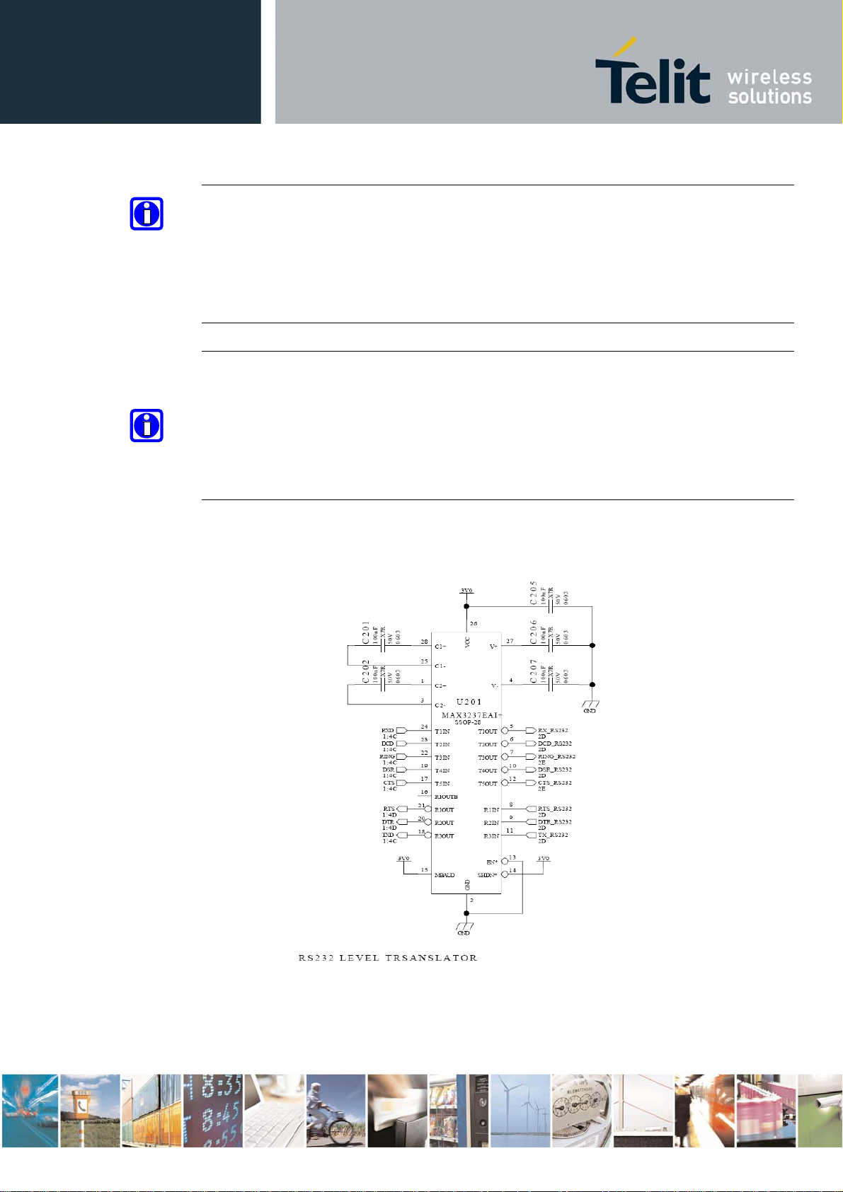
GE/GC864-QUAD V2 and GE864-GPS Hardware User Guide
1vv0300915 Rev.5 – 2011-10-03
NOTE:
The digital input lines working at 2.8V CMOS have an absolute maximum input voltage of
3.0V; therefore the level translator IC shall not be powered by the +3.8V supply of the
module. Instead, it must be powered from a +2.7V / +2.9V (dedicated) power supply.
This is because in this way the level translator IC outputs on the module side (i.e. GE/GC 864
inputs) will work at +3.8V interface levels, damaging the module inputs.
NOTE:
In order to be able to do in circuit reprogramming of the GE/GC 864 firmware, the serial port
on the Telit GE/GC 864 shall be available for translation into RS232 and either it's controlling
device shall be placed into tristate, disconnected or as a gateway for the serial data when
module reprogramming occurs.
Only RXD, TXD, GND and the On/off module turn on pad are required to the reprogramming
of the module, the other lines are unused.
All applicator shall include in their design such a way of reprogramming the GE/GC 864.
An example of level translation circuitry of this kind is:
Reproduction forbidden without Telit Communications S.p.A. written authorization - All Rights Reserved. Page 58 of 94
Page 59

GE/GC864-QUAD V2 and GE864-GPS Hardware User Guide
The RS232 serial port lines are usually connected to a DB9 connector with the following
layout:
9.4. 5V UART Level Translation
1vv0300915 Rev.5 – 2011-10-03
If the OEM application uses a microcontroller with a serial port (UART) that works at a
voltage different from 2.8 – 3V, then a circuitry has to be provided to adapt the different
levels of the two set of signals. As for the RS232 translation there are a multitude of single
chip translators. For example a possible translator circuit for a 5V
TRANSMITTER/RECEIVER can be:
TIP:
Note that the TC7SZ07AE has open drain output; therefore the resistor R2 is mandatory.
Reproduction forbidden without Telit Communications S.p.A. written authorization - All Rights Reserved. Page 59 of 94
Page 60

GE/GC864-QUAD V2 and GE864-GPS Hardware User Guide
1vv0300915 Rev.5 – 2011-10-03
NOTE:
The UART input line TXD (rx_uart) of the GE/GC864-QUAD V2 and GE864-GPS NOT
internally pulled up with a resistor, so there may be the need to place an external 47K pullup resistor, either the DTR (dtr_uart) and RTS (rts_uart) input lines are not pulled up
internally, so an external pull-up resistor of 47K may be required.
Care must be taken to avoid latch-up on the GE/GC864-QUAD V2 and GE864-GPS and the
use of this output line to power electronic devices shall be avoided, especially for devices that
generate spikes and noise such as switching level translators, micro controllers, failure in any
of these condition can severely compromise the GE/GC864-QUAD V2 and GE864-GPS
functionality.
NOTE:
In case of reprogramming of the module has to be considered the use of the RESET line to
start correctly the activity.
The preferable configuration is having an external supply for the buffer level translator.
Reproduction forbidden without Telit Communications S.p.A. written authorization - All Rights Reserved. Page 60 of 94
Page 61

GE/GC864-QUAD V2 and GE864-GPS Hardware User Guide
10. Audio Section Overview
The first Baseband chip was developed for the cellular phones, which needed two separated
amplifiers both in RX and in TX section.
A couple of amplifiers had to be used with internal audio transducers while the other couple
of amplifiers had to be used with external audio transducers.
To distinguish the schematic signals and the Software identifiers, two different definitions
were introduced, with the following meaning:
internal audio transducers HS/MT (from HandSet or MicroTelephone )
external audio transducers HF (from HandsFree )
Actually the acronyms have not the original importance.
1vv0300915 Rev.5 – 2011-10-03
In other words this distinction is not necessary, being the performances between the two
blocks like the same.
Only if the customer needs higher output power to drive the speaker, he needs to adopt the
Aduio2 Section ( HF ) . Otherwise the choice could be done in order to overcome the PCB
design difficulties.
For these reasons we have not changed the HS and HF acronyms, keeping them in the
Software and on the schematics.
The Base Band Chip of the GE864-QUAD V2 Telit Modules maintains the same architecture.
For more information and suggestions refer to Telit document:
Audio settings application note , 80000NT10007a
10.1. Selection mode
Only one block can be active at a time, and the activation of the requested audio path is done
via hardware, by AXE line, or via software ,by AT#CAP command .
Moreover the Sidetone functionality could be implemented by the amplifier fitted between the
transmit path and the receive path, enabled at request in both modes.
Reproduction forbidden without Telit Communications S.p.A. written authorization - All Rights Reserved. Page 61 of 94
Page 62
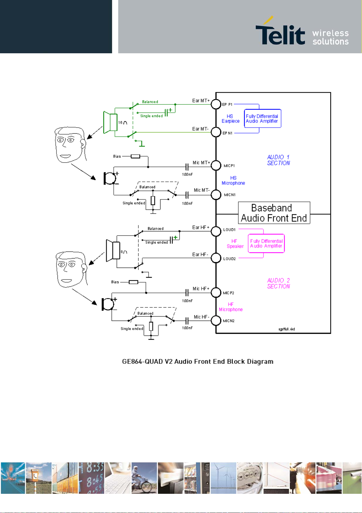
GE/GC864-QUAD V2 and GE864-GPS Hardware User Guide
1vv0300915 Rev.5 – 2011-10-03
Reproduction forbidden without Telit Communications S.p.A. written authorization - All Rights Reserved. Page 62 of 94
Page 63

GE/GC864-QUAD V2 and GE864-GPS Hardware User Guide
10.2. Electrical Characteristics
TIP:
Being the microphone circuitry the more noise sensitive, its design and layout must be done
with particular care. Both microphone paths are balanced and the OEM circuitry must be
balanced designed to reduce the common mode noise typically generated on the ground plane.
However the customer can use the unbalanced circuitry for its particular application.
10.2.1. Input Lines Characteristics
1vv0300915 Rev.5 – 2011-10-03
“MIC_MT” and “MIC_HF” differential microphone paths
Line Coupling AC*
Line Type Balanced
Differential input voltage 1,03V
Gain steps 7
Gain increment 6dB per step
Coupling capacitor 100nF
Differential input resistance 50K
Input capacitance 10pF
(*) WARNING :
AC means that the signals from the microphone have to be connected to input lines of the
module through capacitors which value has to be 100nF. Not respecting this constraint, the
input stages will be damaged.
WARNING:
when particular OEM application needs a Single Ended Input configuration, it is forbidden
connecting the unused input directly to Ground, but only through a 100nF capacitor. Don’t
forget that the useful input signal will be halved in Single Ended Input configuration.
@ Mic G=0dB
pp
Reproduction forbidden without Telit Communications S.p.A. written authorization - All Rights Reserved. Page 63 of 94
Page 64

GE/GC864-QUAD V2 and GE864-GPS Hardware User Guide
10.2.2. Output Lines Characteristics
TIP:
We suggest driving the load differentially from both output drivers, thus the output swing will
double and the need for the output coupling capacitor avoided. However if particular OEM
application needs also a Single Ended circuitry can be implemented, but the output power will
be reduced four times.
The OEM circuitry shall be designed to reduce the common mode noise typically generated
on the ground plane and to get the maximum power output from the device (low resistance
tracks).
1vv0300915 Rev.5 – 2011-10-03
WARNING:
The loads are directly connected to the amplifier outputs when in Differential configuration,
through a capacitor when in Single Ended configuration. Using a Single Ended configuration,
the unused output line must be left open. Not respecting this constraint, the output stage will
be damaged.
TIP :
Remember that there are slightly different electrical performances between the two internal
audio amplifiers:
the “Ear_MT” lines can directly drive a 16Ω load at –12dBFS (**) in Differential
configuration
the “Ear_HF” lines can directly drive a 4Ω load in Differential configurations
There is no difference if the amplifiers drive an external amplifier
(**) 0dBFS is the normalized overall Analog Gain for each Output channel equal to 3,7V
pp
differential
Reproduction forbidden without Telit Communications S.p.A. written authorization - All Rights Reserved. Page 64 of 94
Page 65

GE/GC864-QUAD V2 and GE864-GPS Hardware User Guide
1vv0300915 Rev.5 – 2011-10-03
“EAR_MT” Output Lines
line coupling
0dBFS normalized gain 3,7 V
output load resistance 16 @ -12dBFS
internal output resistance 4 (
signal bandwidth 150 - 4000 Hz @ -3 dB
maximal full scale
differential output voltage
differential output voltage 925mVpp / R
volume increment 2 dB per step
volume steps 10
“EAR_HF” Output Lines
line coupling
output load resistance 8
signal bandwidth 150 - 4000 Hz @ -3 dB
maximal output power
@ battery voltage 3,6V
volume increment 2 dB per step
volume steps 10
AC single-ended
DC differential
differential
pp
typical
)
3,7 V
R
(
typical
pp
load
=open circuit
)
load
=16
@ -12dBFS
AC single-ended
DC differential
0.35 W
rms
/8
Reproduction forbidden without Telit Communications S.p.A. written authorization - All Rights Reserved. Page 65 of 94
Page 66
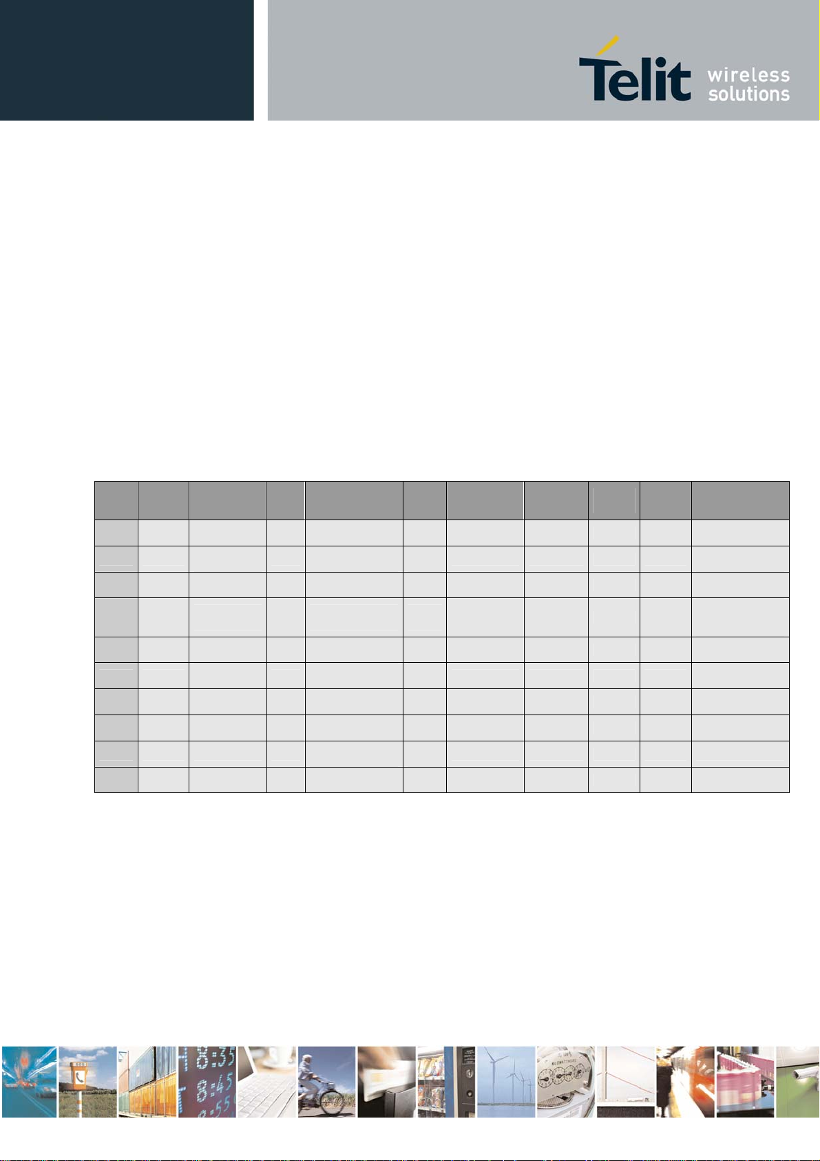
GE/GC864-QUAD V2 and GE864-GPS Hardware User Guide
11. General Purpose I/O
The general-purpose I/O pads can be configured to act in three different ways:
Input
Output
Alternate function (internally controlled)
Input pads can only be read and report the digital value (high or low) present on the pad at the
read time; output pads can only be written or queried and set the value of the pad output; an
alternate function pad is internally controlled by the GE/GC864-QUAD V2 and GE864GPSfirmware and acts depending on the function implemented.
The following GPIO are available on the GE/GC864-QUAD V2 and GE864-GPS:
1vv0300915 Rev.5 – 2011-10-03
Ball
GE864
C1 70
E6 74
C2 66
B3 59
K8 78
B5 68
L9 73
K11 67
C9 76
H3 63
Pin
GC864
Signal I/O Function Type
TGPIO_01 I/O
TGPIO_02 /
JDR
TGPIO_03 I/O
TGPIO_04 /
TXCNTRL
TGPIO_05 /
RFTXMON
TGPIO_06 /
ALARM
TGPIO_07 /
BUZZER
TGPIO_08 I/O
TGPIO_09 I/O
TGPIO_10 /
DVI_TX
GPIO01
Configurable GPIO
GPIO02
I/O
Configurable GPIO
GPIO03
Configurable GPIO
GPIO04
I/O
Configurable GPIO
GPIO05
I/O
Configurable GPIO
GPIO06
I/O
Configurable GPIO
GPIO07
I/O
Configurable GPIO
GPIO08
Configurable GPIO
GPIO09
Configurable GPIO
GPIO10
I/O
Configurable GPIO
CMOS
2.8V
CMOS
2.8V
CMOS
2.8V
CMOS
2.8V
CMOS
2.8V
CMOS
2.8V
CMOS
2.8V
CMOS
2.8V
CMOS
2.8V
CMOS
2.8V
Input / output
current
1uA / 1mA INPUT 0 0
1uA / 1mA INPUT 0 0
1uA / 1mA INPUT 0 0
1uA / 1mA INPUT 0 0
1uA / 1mA INPUT 0 0
1uA / 1mA INPUT 0 0
1uA / 1mA INPUT 0 0
1uA / 1mA INPUT 0 0
1uA / 1mA INPUT 0 0
1uA / 1mA INPUT 0 0
Not all GPIO pads support all these three modes:
GPIO2 supports all three modes and can be input, output, Jamming Detect Output
(Alternate function)
Default
state
ON_OF
F state
During
Reset
state
Note
Alternate function
(JDR)
Alternate function
(RF Transmission
Control)
Alternate function
(RFTXMON)
Alternate function
(ALARM)
Alternate function
(BUZZER)
Alternate function
(DVI_TX)
GPIO4 supports all three modes and can be input, output, RF Transmission
Control (Alternate function)
GPIO5 supports all three modes and can be input, output, RFTX monitor output
(Alternate function)
Reproduction forbidden without Telit Communications S.p.A. written authorization - All Rights Reserved. Page 66 of 94
Page 67

GE/GC864-QUAD V2 and GE864-GPS Hardware User Guide
GPIO6 supports all three modes and can be input, output, alarm output (Alternate
function)
GPIO7 supports all three modes and can be input, output, buzzer output
(Alternate function)
11.1. GPIO Logic Levels
Where not specifically stated, all the interface circuits work at 2.8V CMOS logic levels.
The following tables show the logic level specifications used in the GE/GC864-QUAD V2
and GE864-GPSinterface circuits:
Absolute Maximum Ratings –Not Functional
Parameter Min Max
Input level on any
digital pin when on
Input voltage on analog
pins when on
1vv0300915 Rev.5 – 2011-10-03
-0.3V +3.1V
-0.3V +3.0 V
Operating Range – Interface Levels (2.8V CMOS)
Level Min Max
Input high level 2.1V 3.1V
Input low level 0V 0.5V
Output high level 2.2V 3.0V
Output low level 0V 0.35V
11.2. Using a GPIO Pad as INPUT
The GPIO pads, when used as inputs, can be connected to a digital output of another device
and report its status, provided this device has interface levels compatible with the 2.8V
CMOS levels of the GPIO.
If the digital output of the device to be connected with the GPIO input pad has interface levels
different from the 2.8V CMOS, then it can be buffered with an open collector transistor with a
47K pull up to 2.8V, this pull up must be switched off when the module is in off condition.
Reproduction forbidden without Telit Communications S.p.A. written authorization - All Rights Reserved. Page 67 of 94
Page 68

GE/GC864-QUAD V2 and GE864-GPS Hardware User Guide
1vv0300915 Rev.5 – 2011-10-03
11.3. Using a GPIO Pad as OUTPUT
The GPIO pads, when used as outputs, can drive 2.8V CMOS digital devices or compatible
hardware. When set as outputs, the pads have a push-pull output and therefore the pull-up
resistor may be omitted.
The illustration below shows the base circuit of a push-pull stage:
11.4. Using the RF Transmission Control GPIO4
The GPIO4 pin, when configured as RF Transmission Control Input, permits to disable the
Transmitter when the GPIO is set to Low by the application.
In the design is necessary to add a resistor 47K pull up to 2.8V, this pull up must be switched
off when the module is in off condition.
11.5. Using the RFTXMON Output GPIO5
The GPIO5 pin, when configured as RFTXMON Output, is controlled by the GE/GC 864
QUAD V2 module and will rise when the transmitter is active and fall after the transmitter
activity is completed.
There are 2 different modes for this function:
1) Active during all the calls:
For example, if a call is started, the line will be HIGH during all the conversation and it will
be again LOW after hanged up.
The line rises up 300ms before first TX burst and will became again LOW from 500ms to 1s
after last TX burst.
2) Active during all the TX activity:
The GPIO is following the TX bursts
Please refer to the AT User interface manual for additional information on how to enable this
function.
11.6. Using the Alarm Output GPIO6
The GPIO6 pad, when configured as Alarm Output, is controlled by the module and will rise
when the alarm starts and fall after the issue of a dedicated AT command.
Reproduction forbidden without Telit Communications S.p.A. written authorization - All Rights Reserved. Page 68 of 94
Page 69
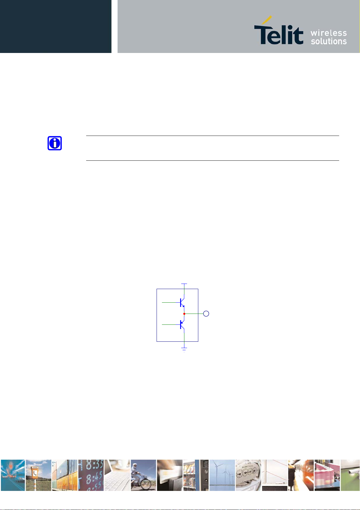
GE/GC864-QUAD V2 and GE864-GPS Hardware User Guide
1vv0300915 Rev.5 – 2011-10-03
This output can be used to power up the module controlling micro controller or application at
the alarm time, giving you the possibility to program a timely system wake-up to achieve
some periodic actions and completely turn off either the application and the module during
sleep periods, dramatically reducing the sleep consumption to few A.
In battery-powered devices this feature will greatly improve the autonomy of the device.
NOTE:
During RESET the line is set to HIGH logic level.
11.7. Using the Buzzer Output GPIO7
The GPIO7 pad, when configured as Buzzer Output, is controlled by the GE/GC 864 QUAD
V2 module and will drive with appropriate square waves a Buzzer driver.
This permits to your application to easily implement Buzzer feature with ringing tones or
melody played at the call incoming, tone playing on SMS incoming or simply playing a tone
or melody when needed by your application.
VDD
Q1
GPIO7
Q2
Reproduction forbidden without Telit Communications S.p.A. written authorization - All Rights Reserved. Page 69 of 94
Page 70

GE/GC864-QUAD V2 and GE864-GPS Hardware User Guide
1vv0300915 Rev.5 – 2011-10-03
A sample interface scheme is included below to give you an idea of how to interface a Buzzer
to the GPIO7:
NOTE:
To correctly drive a buzzer a driver must be provided, its characteristics depend on the Buzzer
and for them refer to your buzzer vendor.
11.8. Using the Temperature Monitor Function
11.8.1. Short Description
The Temperature Monitor is a function of the module that permits to control its internal
temperature and if properly set (see the #TEMPMON command on AT Interface guide) it
raise to High Logic level a GPIO when the maximum temperature is reached.
11.8.2. Allowed GPIO
Ball
GE864
Pin
GC864
Reproduction forbidden without Telit Communications S.p.A. written authorization - All Rights Reserved. Page 70 of 94
Signal I/O Function Type
Input / output
current
Default
state
ON_OF
F state
During
Reset
state
Note
Page 71

C1
E6
C2
B3
K8
B5
L9
K11
C9
H3
70 TGPIO_01 I/O
74
66 TGPIO_03 I/O
59
78
68
73
67 TGPIO_08 I/O
76 TGPIO_09 I/O
63
TGPIO_02 /
JDR
TGPIO_04 /
TXCNTRL
TGPIO_05 /
RFTXMON
TGPIO_06 /
ALARM
TGPIO_07 /
BUZZER
TGPIO_10 /
DVI_TX
I/O
I/O
I/O
I/O
I/O
I/O
GPIO01
Configurable
GPIO
GPIO02
Configurable
GPIO
GPIO03
Configurable
GPIO
GPIO04
Configurable
GPIO
GPIO05
Configurable
GPIO
GPIO06
Configurable
GPIO
GPIO07
Configurable
GPIO
GPIO08
Configurable
GPIO
GPIO09
Configurable
GPIO
GPIO10
Configurable
GPIO
GE/GC864-QUAD V2 and GE864-GPS Hardware User Guide
1vv0300915 Rev.5 – 2011-10-03
CMOS
2.8V
CMOS
2.8V
CMOS
2.8V
CMOS
2.8V
CMOS
2.8V
CMOS
2.8V
CMOS
2.8V
CMOS
2.8V
CMOS
2.8V
CMOS
2.8V
1uA / 1mA INPUT 0 0
1uA / 1mA INPUT 0 0
1uA / 1mA INPUT 0 0
1uA / 1mA INPUT 0 0
1uA / 1mA INPUT 0 0
1uA / 1mA INPUT 0 0
1uA / 1mA INPUT 0 0
1uA / 1mA INPUT 0 0
1uA / 1mA INPUT 0 0
1uA / 1mA INPUT 0 0
Alternate function
(JDR)
Alternate function
(RF Transmission
Control)
Alternate function
(RFTXMON)
Alternate function
(ALARM)
Alternate function
(BUZZER)
Alternate function
(DVI_TX)
The AT#TEMPMON set command could be used with one of the following GPIO:
NOTE:
If the set command is enable the alternate function is not usable.
Reproduction forbidden without Telit Communications S.p.A. written authorization - All Rights Reserved. Page 71 of 94
Page 72

GE/GC864-QUAD V2 and GE864-GPS Hardware User Guide
1vv0300915 Rev.5 – 2011-10-03
11.9. Indication of Network Service Availability
The STAT_LED pin status shows information on the network service availability and Call
status.
In the GE/GC864-QUAD V2 and GE864-GPSmodules, the STAT_LED usually needs an
external transistor to drive an external LED.
Therefore, the status indicated in the following table is reversed with respect to the pin status.
LED status Device Status
Permanently off Device off
Fast blinking
(Period 1s, Ton 0,5s)
Slow blinking
(Period 3s, Ton 0,3s)
Permanently on a call is active
Net search / Not registered /
turning off
Registered full service
A schematic example could be:
Reproduction forbidden without Telit Communications S.p.A. written authorization - All Rights Reserved. Page 72 of 94
Page 73

GE/GC864-QUAD V2 and GE864-GPS Hardware User Guide
1vv0300915 Rev.5 – 2011-10-03
11.10. RTC Bypass Out
The VRTC pin brings out the Real Time Clock supply, which is separate from the rest of the
digital part, allowing having only RTC going on when all the other parts of the device are off.
To this power output a backup capacitor can be added in order to increase the RTC autonomy
during power off of the battery. NO Devices must be powered from this pin.
11.11. External SIM Holder Implementation
Please refer to the related User Guide (SIM Holder Design Guides, 80000NT10001a).
11.12. VAUX Power Output (only for GE864-GPS)
A regulated power supply output is provided in order to supply small devices from the
module.
This output is always active when the module is powered by VBATT.
The operating range characteristics of the supply are:
Operating Range – VAUX1 power supply
Min Typical Max
Output voltage
Output current
Output bypass capacitor
(inside the module)
2.74V 2.80V 2.86V
100mA
1F
Reproduction forbidden without Telit Communications S.p.A. written authorization - All Rights Reserved. Page 73 of 94
Page 74
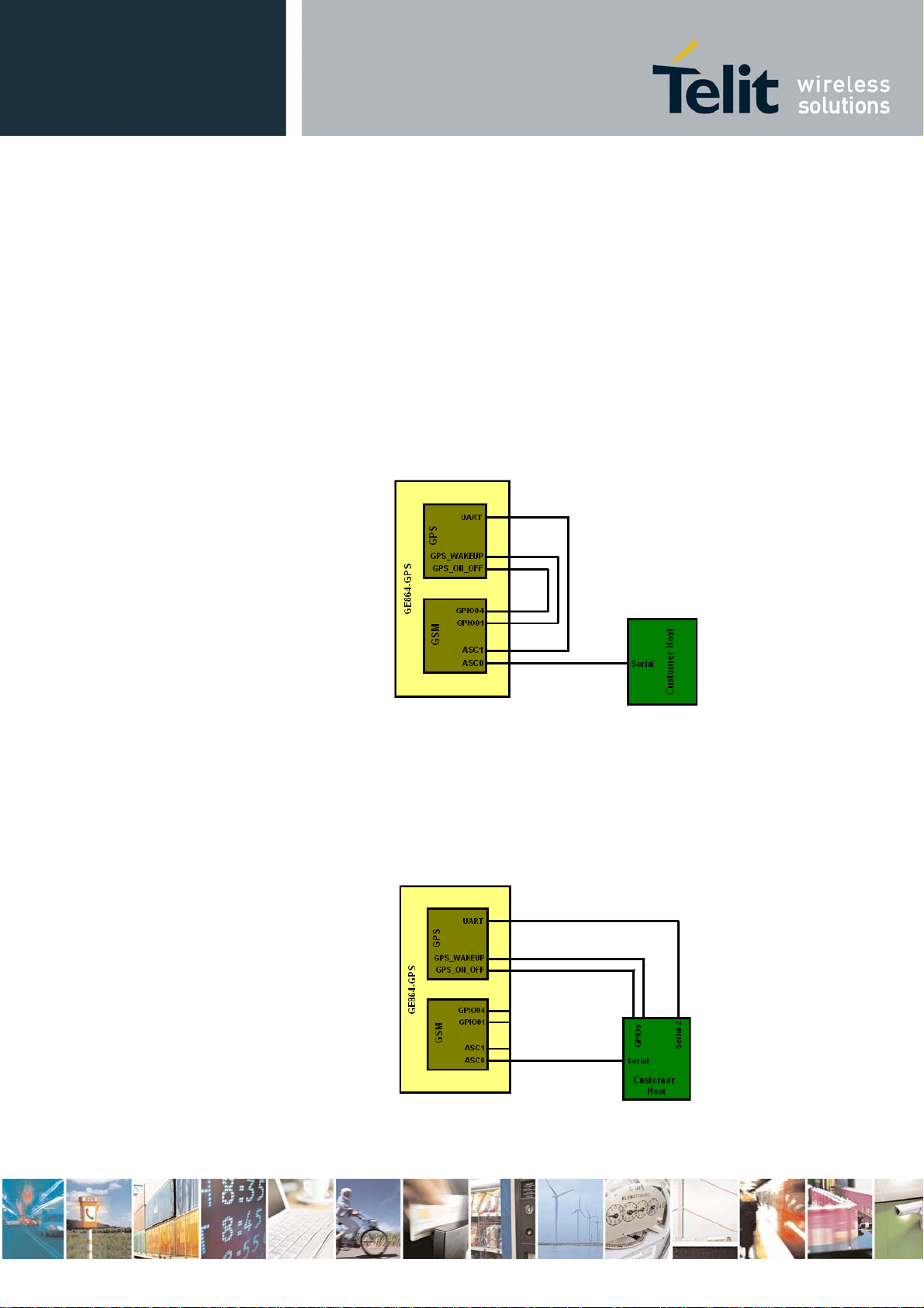
GE/GC864-QUAD V2 and GE864-GPS Hardware User Guide
12. GPS Features (only GE864-GPS)
12.1. GPS Control
The GPS part of GE864-GPS can be driven by the GSM engine or by an external host. The
circuital connections of the two configurations are showed in the subparagraphs below.
12.1.1. GSM Controlled Mode
The GPS part can be controlled by GSM part through specific AT commands (refer to
AT$GPSAT on AT Commands Reference Guide, 80000ST10025a). The required electrical
connections are showed in the figure below.
1vv0300915 Rev.5 – 2011-10-03
12.1.2. External Host Controlled Mode
Alternatively to the previous configuration, the GPS part can be controlled by an external
Host so the GSM and GPS may be managed separately. In this case the Host must have at
least two serial ports and two GPIO available for the control of GPS (see the figure below).
Reproduction forbidden without Telit Communications S.p.A. written authorization - All Rights Reserved. Page 74 of 94
Page 75

GE/GC864-QUAD V2 and GE864-GPS Hardware User Guide
12.2. PPS GPS Output
12.2.1. Description
The Time Mark output GPS_PPS provides a one pulse-per-second signal to the user specific
application. The GPS_PPS pulse is available at any time as soon as a fix is done. This signal
is a positive logic, CMOS level output pulse that transitions from logic 'low' condition to logic
'high' at a 1 Hz rate.
12.2.2. Pulse Characteristics
The signal is available on BGA Ball C8 on GE864-GPS and on pin 24 of PL101 on EVK2
Adapter board.
1vv0300915 Rev.5 – 2011-10-03
Type: Output CMOS 1.8V
Duration: Typically 1us
NOTE:
The signal is available only when the receiver provides a valid Navigation solution.
Reproduction forbidden without Telit Communications S.p.A. written authorization - All Rights Reserved. Page 75 of 94
Page 76

GE/GC864-QUAD V2 and GE864-GPS Hardware User Guide
13. DAC and ADC Converter
13.1. DAC Converter
13.1.1. Description
Ball
GE864
C7 40
The GE/GC864-QUAD V2 AND GE864-GPSmodules provide one Digital to Analog
Converter.
Pin
GC864
Signal I/O Function
DAC Converter
DAC_OUT AO Digital/Analog converter output
1vv0300915 Rev.5 – 2011-10-03
The on board DAC is a 10-bit converter, able to generate an analogue value based a specific
input in the range from 0 up to 1023. However, an external low-pass filter is necessary.
Min Max Units
Voltage range (filtered) 0 2,6 Volt
Range 0 1023 Steps
The precision is 10 bits, so if we consider that the maximum voltage is 2V, the integrated
voltage could be calculated with the following formula:
Integrated output voltage = 2 * value / 1023
DAC_OUT line must be integrated (for example with a low band pass filter) in order to obtain
an analog voltage.
Reproduction forbidden without Telit Communications S.p.A. written authorization - All Rights Reserved. Page 76 of 94
Page 77

13.1.2. Enabling DAC
The AT command below is available to use the DAC function:
AT#DAC[=<enable>[,<value>]]
<value> – scale factor of the integrated output voltage (0–1023, with 10 bit precision), and it
must be present if <enable>=1.
Refer to SW User Guide or AT Commands Reference Guide for the full description of this
function.
Refer to SW User Guide or AT Commands Reference Guide for the full description of this
function.
GE/GC864-QUAD V2 and GE864-GPS Hardware User Guide
1vv0300915 Rev.5 – 2011-10-03
NOTE:
The DAC frequency is selected internally. D/A converter must not be used during
POWERSAVING.
13.1.3. Low Pass Filter Example
Reproduction forbidden without Telit Communications S.p.A. written authorization - All Rights Reserved. Page 77 of 94
Page 78

13.2. ADC Converter
13.2.1. Description
Ball
GE864
J11 37
H11 38
N/A* 39
The GE/GC864-QUAD V2 AND GE864-GPSmodules provide three* (only two in GE864QUAD V2) Analog to Digital Converter.
Pin
GC864
ADC_IN1 AI Analog/Digital converter input
ADC_IN2 AI Analog/Digital converter input
ADC_IN3 AI Analog/Digital converter input
GE/GC864-QUAD V2 and GE864-GPS Hardware User Guide
1vv0300915 Rev.5 – 2011-10-03
Signal I/O Function
ADC Converters
The on board A/D are 11-bit converter. They are able to read a voltage level in the range of
0÷2 volts applied on the ADC pin input, store and convert it into 11 bit word.
Input Voltage range 0 2 Volt
AD conversion - 11 bits
Resolution - < 1 mV
13.2.2. Using ADC Converter
The AT command below is available to use the ADC function:
AT#ADC=1,2
The read value is expressed in mV.
Refer to SW User Guide or AT Commands Reference Guide for the full description of this
function.
Min Max Units
Reproduction forbidden without Telit Communications S.p.A. written authorization - All Rights Reserved. Page 78 of 94
Page 79

GE/GC864-QUAD V2 and GE864-GPS Hardware User Guide
1vv0300915 Rev.5 – 2011-10-03
14. Assembly the GE/GC864-QUAD V2 AND GE864-
GPS on the Board
14.1. Assembly the GE864-QUAD V2
The Telit GE864-QUAD V2 have been designed in order to be compliant with the standard
lead-free SMT process.
Lead-free Alloy:
Surface finishing Sn/Ag/Cu for all solder pads
14.1.1. Recommended foot print for the application
Reproduction forbidden without Telit Communications S.p.A. written authorization - All Rights Reserved. Page 79 of 94
Page 80

14.1.2. Stencil
GE/GC864-QUAD V2 and GE864-GPS Hardware User Guide
1vv0300915 Rev.5 – 2011-10-03
NOTE:
In order to easily rework the GE864-QUAD V2 module is suggested to consider on the
application a 1.5mm inhibit area around the module.
It is also suggested, as common rule for a SMT component, to avoid having a mechanical part
of the application in direct contact with the module.
Stencil apertures layout can be the same of the recommended footprint (1:1), we suggest a
thickness of stencil foil >120µm.
Reproduction forbidden without Telit Communications S.p.A. written authorization - All Rights Reserved. Page 80 of 94
Page 81

14.1.3. PCB pad design
Non solder mask defined” (NSMD) type is recommended for the solder pads on the PCB.
Recommendations for PCB pad dimensions
Ball pitch [mm] 2,5
Solder resist opening diameter A [mm] 1,150
Metal pad diameter B [mm] 1 ± 0.05
It is recommended no microvia without solder resist cover under the module and no microvia
around the pads (see following figure).
GE/GC864-QUAD V2 and GE864-GPS Hardware User Guide
1vv0300915 Rev.5 – 2011-10-03
Holes in pad are allowed only for blind holes and not for through holes.
Reproduction forbidden without Telit Communications S.p.A. written authorization - All Rights Reserved. Page 81 of 94
Page 82

Recommendations for PCB pad surfaces:
Finish Layer thickness [µm] Properties
Electro-less Ni /
Immersion Au
The PCB must be able to resist the higher temperatures which are occurring at the lead-free
process. This issue should be discussed with the PCB-supplier. Generally, the wettability of
tin-lead solder paste on the described surface plating is better compared to lead-free solder
paste.
14.1.4. Solder paste
It is recommended to use only “no clean” solder paste in order to avoid the cleaning of
the modules after assembly.
GE/GC864-QUAD V2 and GE864-GPS Hardware User Guide
3 –7 /
0.05 – 0.15
Solder paste
1vv0300915 Rev.5 – 2011-10-03
good solder ability protection,
high shear force values
Lead free
Sn/Ag/Cu
14.1.5. GE864-QUAD V2/GPS Solder reflow
The following is the recommended solder reflow profile
Reproduction forbidden without Telit Communications S.p.A. written authorization - All Rights Reserved. Page 82 of 94
Page 83

GE/GC864-QUAD V2 and GE864-GPS Hardware User Guide
1vv0300915 Rev.5 – 2011-10-03
Profile Feature Pb-Free Assembly
Average ramp-up rate (TL to TP) 3°C/second max
Preheat
– Temperature Min (Tsmin)
– Temperature Max (Tsmax)
– Time (min to max) (ts)
Tsmax to TL
– Ramp-up Rate
Time maintained above:
– Temperature (TL)
– Time (tL)
Peak Temperature (Tp) 245 +0/-5°C
Time within 5°C of actual Peak
Temperature (tp)
Ramp-down Rate 6°C/second max.
Time 25°C to Peak Temperature 8 minutes max.
150°C
200°C
60-180 seconds
3°C/second max
217°C
60-150 seconds
10-30 seconds
NOTE:
All temperatures refer to topside of the package, measured on the package body surface
WARNING:
The GE864 module withstands one reflow process only.
Reproduction forbidden without Telit Communications S.p.A. written authorization - All Rights Reserved. Page 83 of 94
Page 84

GE/GC864-QUAD V2 and GE864-GPS Hardware User Guide
14.2. Assembly the GC864-QUAD V2
The position of the Molex board to board connector and the pin 1 are shown in the following
picture.
1vv0300915 Rev.5 – 2011-10-03
NOTE:
The metal tabs present on GC864-QUAD V2 must be connected to GND.
This module could not be processed with a reflow.
Reproduction forbidden without Telit Communications S.p.A. written authorization - All Rights Reserved. Page 84 of 94
Page 85

GE/GC864-QUAD V2 and GE864-GPS Hardware User Guide
1vv0300915 Rev.5 – 2011-10-03
14.3. Debug of the GE/GC864-QUAD V2 AND GE864-GPS in
Production
To test and debug the mounting of GC/GE864-QUAD V2 and GE864-GPS , we strongly
recommend to foreseen test pads on the host PCB, in order to check the connection between
the GE/GC864-QUAD V2 and GE864-GPS itself and the application and to test the
performance of the module connecting it with an external computer. Depending by the
customer application, these pads include, but are not limited to the following signals:
Ball GE864 Pin GC864 Signal Function
J1, J2, K1, K2 1,2,3,4
A1, A11, D6, F1, F11,
H1, H2, J3, K3, K4, K5,
K6, L1, L2, L3, L6, L11
E7 25
H8 26
L8 49
J5 53
A2 54
F10 23
D11 24
5,6,7,
46
H4 47
J43
E103
F83
G23
N/A
N/A
N/A
N/A
(3) Available only on GE864-GPS (in case of GE864-QUAD it has to be considered RESERVED)
VBATT Main power supply
GND Ground
C103/TXD Serial data input (TXD) from DTE
C104/RXD Serial data output (RXD) to DTE
PRWMON Power ON Monitor
ON/OFF* Input command for switching power ON or OFF (toggle command).
RESET* Reset input
RX_AUX Auxiliary UART (RX Data from DTE)
TX_AUX Auxiliary UART (TX Data to DTE)
Service pin shall be used to upgrade the module from ASC1
(RX_TRACE, TX_TRACE). The pin shall be tied low to
SERVICE
GPS_ON_OFF
GPS_RX3
GPS_TX3
GPS_WAKEUP
3
enable the feature only in case of a SW Update activity. It is
required, for debug purpose, to be connected
to a test pad on the final application.
3
GPS Power Control
GPS Serial data input
GPS Serial data output
Wake up output3
Reproduction forbidden without Telit Communications S.p.A. written authorization - All Rights Reserved. Page 85 of 94
Page 86

GE/GC864-QUAD V2 and GE864-GPS Hardware User Guide
15. Packing system
15.1. GE864-QUAD V2/GPS Packaging
The GE864-QUAD V2/GPS is packaged on trays of 20 pieces each. This is especially
suitable for the GE864-QUAD V2/GPS according to SMT processes for pick & place
1vv0300915 Rev.5 – 2011-10-03
Section A-A
movement requirements. The size of the tray is: 329 x 176mm.
Reproduction forbidden without Telit Communications S.p.A. written authorization - All Rights Reserved. Page 86 of 94
Page 87

WARNING:
These trays can withstand at the maximum temperature of 65° C.
NOTE:
All temperatures refer to topside of the package, measured on the package body surface
15.1.1. Moisture sensibility
The level of moisture sensibility of the Product is “3”, according with standard IPC/JEDEC JSTD-020, take care of all the relative requirements for using this kind of components.
GE/GC864-QUAD V2 and GE864-GPS Hardware User Guide
1vv0300915 Rev.5 – 2011-10-03
Moreover, the customer has to take care of the following conditions:
a) The shelf life of the Product inside of the dry bag must be 12 months from the bag seal date,
when stored in a non-condensing atmospheric environment of <40°C / 90% RH
b) Environmental condition during the production: 30°C / 60% RH according to
IPC/JEDEC J-STD-033A paragraph 5
c) The maximum time between the opening of the sealed bag and the reflow process must be
168 hours if condition b) “IPC/JEDEC J-STD-033A paragraph 5.2” is respected
d) Baking is required if conditions b) or c) are not respected
e) Baking is required if the humidity indicator inside the bag indicates 10% RH or more
Reproduction forbidden without Telit Communications S.p.A. written authorization - All Rights Reserved. Page 87 of 94
Page 88

GE/GC864-QUAD V2 and GE864-GPS Hardware User Guide
15.1.2. GE864 orientation on the tray
1vv0300915 Rev.5 – 2011-10-03
Reproduction forbidden without Telit Communications S.p.A. written authorization - All Rights Reserved. Page 88 of 94
Page 89

GE/GC864-QUAD V2 and GE864-GPS Hardware User Guide
1vv0300915 Rev.5 – 2011-10-03
15.2. GE/GC864-QUAD V2 AND GE864-GPS Packaging
The Telit GC864-QUAD V2 are packaged on trays of 20 pieces each.
The size of the tray is: 329 x 176mm.
WARNING:
These trays can withstand at the maximum temperature of 65° C.
Reproduction forbidden without Telit Communications S.p.A. written authorization - All Rights Reserved. Page 89 of 94
Page 90

GE/GC864-QUAD V2 and GE864-GPS Hardware User Guide
16. Conformity Assessment Issues
The Telit GE/GC864-QUAD V2 and GE864-GPS has been
assessed in order to satisfy the essential requirements of the
R&TTE Directive 1999/05/EC (Radio Equipment &
Telecommunications Terminal Equipments) to demonstrate the
conformity against the harmonised standards with the final
involvement of a Notified Body.
If the module is installed in conformance to the Telit installation manuals, no further
evaluation under Article 3.2 of the R&TTE Directive and do not require further involvement
of a R&TTE Directive Notified Body for the final product.
In all other cases, or if the manufacturer of the final product is in doubt, then the equipment
integrating the radio module must be assessed against Article 3.2 of the R&TTE Directive.
In all cases the assessment of the final product must be made against the Essential
requirements of the R&TTE Directive Articles 3.1(a) and (b), Safety and EMC respectively,
and any relevant Article 3.3 requirements.
This Hardware User Guide contains all the information you may need for developing a
product meeting the R&TTE Directive.
1vv0300915 Rev.5 – 2011-10-03
Reproduction forbidden without Telit Communications S.p.A. written authorization - All Rights Reserved. Page 90 of 94
Page 91

GE/GC864-QUAD V2 and GE864-GPS Hardware User Guide
17. SAFETY RECOMMANDATIONS
READ CAREFULLY
Be sure the use of this product is allowed in the country and in the environment required. The
use of this product may be dangerous and has to be avoided in the following areas:
Where it can interfere with other electronic devices in environments such as hospitals,
airports, aircrafts, etc
Where there is risk of explosion such as gasoline stations, oil refineries, etc
It is responsibility of the user to enforce the country regulation and the specific environment
regulation.
Do not disassemble the product; any mark of tampering will compromise the warranty
validity.
We recommend following the instructions of the hardware user guides for a correct wiring of
the product. The product has to be supplied with a stabilized voltage source and the wiring
has to be conforming to the security and fire prevention regulations.
The product has to be handled with care, avoiding any contact with the pins because
electrostatic discharges may damage the product itself. Same cautions have to be taken for the
SIM, checking carefully the instruction for its use. Do not insert or remove the SIM when the
product is in power saving mode.
The system integrator is responsible of the functioning of the final product; therefore, care has
to be taken to the external components of the module, as well as of any project or installation
issue, because the risk of disturbing the GSM network or external devices or having impact
on the security. Should there be any doubt, please refer to the technical documentation and the
regulations in force.
Every module has to be equipped with a proper antenna with specific characteristics. The
antenna has to be installed with care in order to avoid any interference with other electronic
devices and has to guarantee a minimum distance from the body (20 cm). In case of this
requirement cannot be satisfied, the system integrator has to assess the final product against
the SAR regulation.
The European Community provides some Directives for the electronic equipments introduced
on the market. All the relevant information’s are available on the European Community
website:
http://ec.europa.eu/enterprise/sectors/rtte/documents/
1vv0300915 Rev.5 – 2011-10-03
Reproduction forbidden without Telit Communications S.p.A. written authorization - All Rights Reserved. Page 91 of 94
Page 92

GE/GC864-QUAD V2 and GE864-GPS Hardware User Guide
1vv0300915 Rev.5 – 2011-10-03
The text of the Directive 99/05 regarding telecommunication equipments is available, while
the applicable Directives (Low Voltage and EMC) are available at:
http://ec.europa.eu/enterprise/sectors/electrical
FCC Regulatory Requirements
This device complies with Part 15 of the FCC Rules. Operation is subject to the
following two conditions:
(1) this device may not cause harmful interference, and
(2) this device must accept any interference received, including interference that may
cause undesired operation.
RF Exposure:
The antenna(s) used for this transmitter must be installed to provide a separation
distance of at least 20 cm from all the persons and must not be co-located or operating
in conjunction with any other antenna or transmitter.
The system antenna(s) used for this module must not exceed 1,4dBi (850MHz) and
3.0dBi (1900MHz) for mobile and fixed or mobile operating configurations.
Users and installers must be provided with antenna installation instructions and
transmitter operating conditions for satisfying RF exposure compliance.
A label containing the following information must be affixed to the outside of a host
product which incorporates this module:
Label Module type
Contains FCC ID: RI7GE86Q2 For GE864-QUAD V2
Contains FCC ID: RI7GC864Q2 For CE864-QUAD V2
Contains FCC ID: RI7GE864G2 For GE864-GPS
IC Regulatory Requirements
This device complies with Industry Canada license-exempt RSS standard(s).
Operation is subject to the following two conditions:
(1) this device may not cause interference, and
(2) this device must accept any interference, including interference that may cause
undesired operation of the device.
Le présent appareil est conforme aux CNR d'Industrie Canada applicables aux
appareils radio exempts de licence. L'exploitation est autorisée aux deux conditions
suivantes :
(1) l'appareil ne doit pas produire de brouillage, et
Reproduction forbidden without Telit Communications S.p.A. written authorization - All Rights Reserved. Page 92 of 94
Page 93

GE/GC864-QUAD V2 and GE864-GPS Hardware User Guide
1vv0300915 Rev.5 – 2011-10-03
(2) l'utilisateur de l'appareil doit accepter tout brouillage radioélectrique subi, même
si le brouillage est susceptible d'en compromettre le fonctionnement.
Under Industry Canada regulations, this radio transmitter may only operate using an
antenna of a type and maximum (or lesser) gain approved for the transmitter by
Industry Canada. To reduce potential radio interference to other users, the antenna
type and its gain should be so chosen that the equivalent isotropically radiated power
(e.i.r.p.) is not more than that necessary for successful communication.
Conformément à la réglementation d'Industrie Canada, le présent émetteur radio peut
fonctionner avec une antenne d'un type et d'un gain maximal (ou inférieur) approuvé
pour l'émetteur par Industrie Canada. Dans le but de réduire les risques de brouillage
radioélectrique à l'intention des autres utilisateurs, il faut choisir le type d'antenne et
son gain de sorte que la puissance isotrope rayonnée équivalente (p.i.r.e.) ne dépasse
pas l'intensité nécessaire à l'établissement d'une communication satisfaisante.
The
GE/GC864-QUAD V2 and GE864-GPS
has been designed to comply with safety
requirements for exposure to radio waves (SAR) in accordance with RSS-102. Please
follow the instructions included in the user guide for product installation and use.
This radio transmitter
GE/GC864-QUAD V2 and GE864-GPS
has been approved by
Industry Canada to operate with antennas with maximum permissible gain not
exceeding 1,4dBi (850MHz) and 3.0dBi (1900MHz).
Antenna types having a gain greater than the maximum gain indicated are strictly
prohibited for use with this device.
Le
GE/GC864-QUAD V2 and GE864-GPS
a été conçu pour se conformer aux exigences
de sécurité pour l'exposition aux ondes radio (SAR) en conformité avec RSS-102. S'il
vous plaît suivez les instructions incluses dans le guide utilisateur pour l'installation
du produit et son utilisation.
Cet émetteur radio (numéro de modèle) a été approuvé par Industrie Canada pour
fonctionner avec des antennes avec un gain maximal admissible de 1.4 dBi (850MHz)
et 3.0dBi (1900MHz).
Types d'antenne ayant un gain supérieur au gain maximal indiqué est strictement
interdit pour une utilisation avec cet appareil.
Reproduction forbidden without Telit Communications S.p.A. written authorization - All Rights Reserved. Page 93 of 94
Page 94

R
g
GE/GC864-QUAD V2 and GE864-GPS Hardware User Guide
18. Document History
1vv0300915 Rev.5 – 2011-10-03
Reevviissiioonn
Rev.0 2011-01-14 First preliminary release
Rev.1 2011-04-07 Updated power consumption for GE864-GPS and ATEX data for GE864-GPS
Rev.2 2011-06-15
Rev.4 2011-08-24 Added chapter 7.2 PCB guidelines in case of FCC certifications – updated with FCC
Rev.5 2011-10-03
DDaattee
geess
n
CChhaan
Updated Pin Out GE864 QUAD/GPS
Added “5.4 Turning ON/OFF the GPS (only GE864-GPS)” paragraph
Updated GPS Antenna Requirements
Updated Logic Level Specifications
Added “11.12 VAUX Power Output (only for GE864-GPS)” paragraph
Added “12. GPS Features (GE864-GPS only)” Chapter
requirements
Added chapter 17. Safety Recommendations – updated with FCC and IC requirements
Chapter 4: pin-out table, C6 and G6 rows moved under “GPS” category; notes re-organized; C6
and G6 pins added in the table at page 19; BGA balls layout, C6 and G6 balls colored in orange
and wording “Diagnostic” added.
Chapter 14.1.3 PCB pad design – table – ball pitch errata corridge from 2,4 to 2,5
Chapter 15.1.1 Moisture sensibility – add details
Updated Chapter 5.1 Turning ON the Module – 5 second with VBATT< 3,4V
Reproduction forbidden without Telit Communications S.p.A. written authorization - All Rights Reserved. Page 94 of 94
 Loading...