

Telit Wireless Solutions GainSpan GS2K Series, GainSpan GS2100M, GainSpan GS2011M, GainSpan GS2101M, GainSpan GS2200M Hardware User's Manual
Page 1

GS2K Module Evaluation Board Hardware User Guide
GS2K Module Evaluation Board
Hardware User Guide
1VV0301435 Rev. 1.5 – 2018-12-11
Page 2

GS2K Module Evaluation Board Hardware User Guide
SPECIFICATIONS ARE SUBJECT TO CHANGE WITHOUT NOTICE
NOTICE
While reasonable efforts have been made to assure the accuracy of this document, Telit
assumes no liability resulting from any inaccuracies or omissions in this document, or from
use of the information obtained herein. The information in this document has been carefully
checked and is believed to be reliable. However, no responsibility is assumed for
inaccuracies or omissions. Telit reserves the right to make changes to any products
described herein and reserves the right to revise this document and to make changes from
time to time in content hereof with no obligation to notify any person of revisions or changes.
Telit does not assume any liability arising out of the application or use of any product,
software, or circuit described herein; neither does it convey license under its patent rights or
the rights of others.
It is possible that this publication may contain references to, or information about Telit
products (machines and programs), programming, or services that are not announced in your
country. Such references or information must not be construed to mean that Telit intends to
announce such Telit products, programming, or services in your country.
COPYRIGHTS
This instruction manual and the Telit products described in this instruction manual may be,
include or describe copyrighted Telit material, such as computer programs stored in
semiconductor memories or other media. Laws in the Italy and other countries preserve for
Telit and its licensors certain exclusive rights for copyrighted material, including the exclusive
right to copy, reproduce in any form, distribute and make derivative works of the copyrighted
material. Accordingly, any copyrighted material of Telit and its licensors contained herein or in
the Telit products described in this instruction manual may not be copied, reproduced,
distributed, merged or modified in any manner without the express written permission of Telit.
Furthermore, the purchase of Telit products shall not be deemed to grant either directly or by
implication, estoppel, or otherwise, any license under the copyrights, patents or patent
applications of Telit, as arises by operation of law in the sale of a product.
COMPUTER SOFTWARE COPYRIGHTS
The Telit and 3rd Party supplied Software (SW) products described in this instruction manual
may include copyrighted Telit and other 3rd Party supplied computer programs stored in
semiconductor memories or other media. Laws in the Italy and other countries preserve for
Telit and other 3rd Party supplied SW certain exclusive rights for copyrighted computer programs, including the exclusive right to copy or reproduce in any form the copyrighted computer program. Accordingly, any copyrighted Telit or other 3rd Party supplied SW computer
programs contained in the Telit products described in this instruction manual may not be copied (reverse engineered) or reproduced in any manner without the express written permission
of Telit or the 3rd Party SW supplier. Furthermore, the purchase of Telit products shall not be
deemed to grant either directly or by implication, estoppel, or otherwise, any license under the
copyrights, patents or patent applications of Telit or other 3rd Party supplied SW, except for
the normal non-exclusive, royalty free license to use that arises by operation of law in the sale
of a product.
1VV0301435 Rev. 1.5 2 2018-12-11
Page 3

GS2K Module Evaluation Board Hardware User Guide
USAGE AND DISCLOSURE RESTRICTIONS
I. License Agreements
The software described in this document is the property of Telit and its licensors. It is
furnished by express license agreement only and may be used only in accordance with the
terms of such an agreement.
II. Copyrighted Materials
Software and documentation are copyrighted materials. Making unauthorized copies is
prohibited by law. No part of the software or documentation may be reproduced, transmitted,
transcribed, stored in a retrieval system, or translated into any language or computer
language, in any form or by any means, without prior written permission of Telit
III. High Risk Materials
Components, units, or third-party products used in the product described herein are NOT
fault-tolerant and are NOT designed, manufactured, or intended for use as on-line control
equipment in the following hazardous environments requiring fail-safe controls: the operation
of Nuclear Facilities, Aircraft Navigation or Aircraft Communication Systems, Air Traffic
Control, Life Support, or Weapons Systems (High Risk Activities"). Telit and its supplier(s)
specifically disclaim any expressed or implied warranty of fitness for such High Risk Activities.
IV. Trademarks
TELIT and the Stylized T Logo are registered in Trademark Office. All other product or service
names are the property of their respective owners.
V. Third Party Rights
The software may include Third Party Right software. In this case you agree to comply with all
terms and conditions imposed on you in respect of such separate software. In addition to
Third Party Terms, the disclaimer of warranty and limitation of liability provisions in this
License shall apply to the Third Party Right software.
TELIT HEREBY DISCLAIMS ANY AND ALL WARRANTIES EXPRESS OR IMPLIED FROM
ANY THIRD PARTIES REGARDING ANY SEPARATE FILES, ANY THIRD PARTY
MATERIALS INCLUDED IN THE SOFTWARE, ANY THIRD PARTY MATERIALS FROM
WHICH THE SOFTWARE IS DERIVED (COLLECTIVELY “OTHER CODE”), AND THE USE
OF ANY OR ALL THE OTHER CODE IN CONNECTION WITH THE SOFTWARE,
INCLUDING (WITHOUT LIMITATION) ANY WARRANTIES OF SATISFACTORY QUALITY
OR FITNESS FOR A PARTICULAR PURPOSE.
NO THIRD PARTY LICENSORS OF OTHER CODE SHALL HAVE ANY LIABILITY FOR ANY
DIRECT, INDIRECT, INCIDENTAL, SPECIAL, EXEMPLARY, OR CONSEQUENTIAL
DAMAGES (INCLUDING WITHOUT LIMITATION LOST PROFITS), HOWEVER CAUSED
AND WHETHER MADE UNDER CONTRACT, TORT OR OTHER LEGAL THEORY,
ARISING IN ANY WAY OUT OF THE USE OR DISTRIBUTION OF THE OTHER CODE OR
THE EXERCISE OF ANY RIGHTS GRANTED UNDER EITHER OR BOTH THIS LICENSE
AND THE LEGAL TERMS APPLICABLE TO ANY SEPARATE FILES, EVEN IF ADVISED
OF THE POSSIBILITY OF SUCH DAMAGES.
1VV0301435 Rev. 1.5 3 2018-12-11
Page 4

GS2K Module Evaluation Board Hardware User Guide
APPLICABILITY TABLE
PRODUCT
GS2K based Modules
Board Revision
EVB1.1, EVB 2.0, EVB 3.0
and EVB 3.1
Note: The features described in the present document are provided by the products equipped
with the software versions equal or higher than the versions shown in the table. See also
the Revision History section.
1VV0301435 Rev. 1.5 4 2018-12-11
Page 5

GS2K Module Evaluation Board Hardware User Guide
Table of Contents
Chapter 1 Hardware Overview ........................................................................................................ 18
1.1 GainSpan GS2011M Ultra-Low Power 802.11b/g/n Module .................................................18
1.1.1 GS2011M Module Evaluation Board ............................................................................ 19
1.2 GainSpan GS2100M Low Power 802.11b/g/n Module .......................................................... 24
1.2.1 GS2100M Module Evaluation Board ............................................................................ 25
1.3 GainSpan GS2101M Ultra-Low Power 802.11b/g/n Module .................................................30
1.3.1 GS2101M Module Evaluation Board ............................................................................ 31
1.4 GainSpan GS2200M Ultra-Low Power 802.11b/g/n Module .................................................34
1.4.1 GS2200M Module Evaluation Board ............................................................................ 34
1.5 Evaluation Board Software .................................................................................................... 37
Chapter 2 Setting Up the Evaluation Board .....................................................................................38
2.1 Preparing for Evaluation Board Setup ...................................................................................38
2.1.1 Site Preparation ........................................................................................................... 39
2.1.2 Safety Guidelines and Standards ................................................................................. 39
2.1.3 Environmental Requirements ....................................................................................... 39
2.1.4 Unpacking and Inspecting the GS2000 Based Module Evaluation Board ...................40
2.2 Setting Up the GS2000 Based Module Evaluation Board .....................................................41
2.2.1 Placing the GS2000 Based Module Evaluation Board on a Tabletop ..........................41
2.3 Power Guidelines, Requirements, and Safety Specifications ................................................ 42
2.3.1 Electrical Guidelines ..................................................................................................... 42
2.3.2 Connecting Power ........................................................................................................42
Chapter 3 Initial Board Connections and Configuration ................................................................... 43
3.1 Connecting the Board to a Communication Port ...................................................................43
3.2 Providing Power to the Evaluation Board ..............................................................................46
3.2.1 Connecting Power to the Board ................................................................................... 46
3.3 Configuring the Board for Wireless Network ......................................................................... 48
3.3.1 Connect to a Network ...................................................................................................48
Appendix A GS2000 Evaluation Board Specifications ..................................................................... 50
A.1 GS2011M Evaluation Board Specifications ..........................................................................50
A.2 GS2011M Evaluation Board LEDs ........................................................................................ 51
A.3 GS2011M Evaluation Board Sensors ...................................................................................53
A.4 GS2011M Evaluation Board Switches .................................................................................. 53
A.5 GS2011M Evaluation Board Jumper Settings ....................................................................... 54
A.6 GS2100M Evaluation Board Specifications ..........................................................................56
A.7 GS2100M Evaluation Board LEDs ........................................................................................ 57
A.8 GS2100M Evaluation Board Switches .................................................................................. 58
A.9 GS2100M Evaluation Board Jumper Settings ....................................................................... 59
A.10 GS2101M Evaluation Board Specifications ........................................................................60
A.11 GS2101M Evaluation Board LEDs ...................................................................................... 61
A.12 GS2101M Evaluation Board Switches ................................................................................ 62
A.13 GS2101M Evaluation Board Jumper Settings ..................................................................... 63
A.14 GS2200M Evaluation Board Specifications ........................................................................64
A.15 GS2200M Evaluation Board LEDs ...................................................................................... 65
A.16 GS2200M Evaluation Board Sensors ................................................................................. 66
A.17 GS2200M Evaluation Board Switches ................................................................................ 66
A.18 GS2200M Evaluation Board Jumper Settings ..................................................................... 67
1VV0301435 Rev. 1.5 5 2018-12-11
Page 6

GS2K Module Evaluation Board Hardware User Guide
Appendix B Connector Pinouts ........................................................................................................ 68
B.1 GS2011M, GS2100M, GS2101M and GS2200M JTAG Cortex Debug Connector Pinouts .68
B.2 GS2011M, GS2100M, GS2101M and GS2200M SPI0 Connector Pinouts .......................... 69
B.3 GS2011M, GS2100M, GS2101M and GS2200M SDIO Test Connector Pinouts ................. 70
B.4 GS2011M Evaluation Board Pinouts .....................................................................................71
B.4.1 GS2011M Daughter Board Header Connector Pinouts ............................................... 71
B.4.2 GS2011M Test Point Header Connector Pinouts ........................................................75
B.5 GS2100M Evaluation Board Pinouts .....................................................................................77
B.5.1 GS2100M Daughter Board Header Connector Pinouts ............................................... 77
B.5.2 GS2100M Analog Digital Converter Terminal Connector ............................................80
B.6 GS2101M Evaluation Board Pinouts .....................................................................................81
B.6.1 GS2101M Daughter Board Header Connector Pinouts ............................................... 81
B.6.2 GS2101M Analog Digital Converter Terminal Connector ............................................82
B.6.3 GS2101M Analog Digital Converter Terminal and Header .......................................... 83
B.7 GS2200M Evaluation Board Pinouts .....................................................................................84
B.7.1 GS2200M Daughter Board Header Connector Pinouts ............................................... 84
B.7.2 GS2200M Analog Digital Converter Terminal Header ................................................. 86
1VV0301435 Rev. 1.5 6 2018-12-11
Page 7

GS2K Module Evaluation Board Hardware User Guide
About This Manual
This manual provides guidelines for setting up and using the GainSpan® GS2000 based
module evaluation board that supports the GS2011M, GS2100M, GS2101M and GS2200M
modules.
Refer to the following sections:
• Revision History, page 8
• Audience, page 8
• Standards, page 8
• Documentation Conventions, page 9
• Documentation, page 12
• References, page 14
• Contact Information, Support, page 15
• Returning Products to Telit, page 16
• Accessing the Telit Wi-Fi Portal, page 17
1VV0301435 Rev. 1.5 7 2018-12-11
Page 8

GS2K Module Evaluation Board Hardware User Guide
Revision History
This version of the GS2000 Based Module Evaluation Board Hardware User Guide
contains the following new information listed in Table 1, page 8.
Version Date Remarks
1.0 November 2013 Initial Release
1.1 February 2014
1.2 November 2014
Table 1 Revision History
Updated GS2011M and GS2100M specifications.
See A.1 GS2011M Evaluation Board Specifications,
page 50 and A.6 GS2100M Evaluation Board
Specifications, page 56.
Added supported information for GS2011M and
GS2100M evaluation board Revision 3.0.
GS2011M Evaluation Board Components. See Tab le
7, page 22.
GS2100M Evaluation Board Components. See Table
9, page 28.
Added GS2011M and GS2100M Evaluation Board
Specifications for EVB revision 3.0. See Appendix A
GS2000 Evaluation Board Specifications, page 50.
Added GS2011M and GS2100M Evaluation Board
Connector Pinouts for EVB revision 3.0. See
Appendix B Connector Pinouts, page 68.
Audience
Standards
Added notation specifying the usage of dual UART
1.3 June 2015
1.4 January 2018 Added GS2101M and GS2200M detail.
1.5 December 2018 Updated Telit Contact Information.
This manual provides instructions on how to setup and use the GS2000 based module
evaluation board along with component description, jumper settings, board specifications,
and pinouts.
The standards that are supported by the GS2000 based modules are IEEE 802.11b/g/n.
for the GS2100M EVB. See GS2100M Module
Evaluation Board, page 25.
1VV0301435 Rev. 1.5 8 2018-12-11
Page 9

GS2K Module Evaluation Board Hardware User Guide
Documentation Conventions
This manual uses the following text and syntax conventions:
– Special text fonts represent particular commands, keywords, variables, or window
sessions
– Color text indicates cross-reference hyper links to supplemental information
– Command notation indicates commands, subcommands, or command elements
Table 2, page 9, describes the text conventions used in this manual for software procedures
that are explained using the AT command line interface.
Table 2 Document Text Conventions
Convention Type Description
This monospaced font represents command strings entered on a
command syntax
monospaced font
command line and sample source code.
AT XXXX
Proportional font
description
UPPERCASE
Variable parameter
lowercase
Keyword parameter
[ ]
Square brackets
?
Question mark
<ESC>
Escape sequence
Gives specific details about a parameter.
<Data> DATA
Indicates user input. Enter a value according to the descriptions that
follow. Each uppercased token expands into one or more other token.
Indicates keywords. Enter values exactly as shown in the command
description.
Enclose optional parameters. Choose none; or select one or more an
unlimited number of times each. Do not enter brackets as part of any
command.
[parm1|parm2|parm3]
Used with the square brackets to limit the immediately following token
to one occurrence.
Each escape sequence <ESC> starts with the ASCII character 27 (0x1B).
This is equivalent to the Escape key.
<ESC>C
<CR>
Carriage return
<LF>
Each command is terminated by a carriage return.
Each command is terminated by a line feed.
Line feed
1VV0301435 Rev. 1.5 9 2018-12-11
Page 10

GS2K Module Evaluation Board Hardware User Guide
Table 2 Document Text Conventions (Continued)
Convention Type Description
<CR> <LF>
Carriage return
Line feed
< >
Angle brackets
=
Equal sign
.
dot (period)
A.B.C.D
IP address
X:X::X:X
IPv6 IP address
Each response is started with a carriage return and line feed with some
exceptions.
Enclose a numeric range, endpoints inclusive. Do not enter angle
brackets as part of any command.
<SSID>
Separates the variable from explanatory text. Is entered as part of the
command.
PROCESSID = <CID>
Allows the repetition of the element that immediately follows it multiple
times. Do not enter as part of the command.
.AA:NN can be expanded to 1:01 1:02 1:03.
IPv4-style address.
10.0.11.123
IPv6-style address.
3ffe:506::1
Where the : : represents all 0x for those address components not
explicitly given.
LINE
End-to-line input token
WORD
Single token
Indicates user input of any string, including spaces. No other parameters
may be entered after input for this token.
string of words
Indicates user input of any contiguous string (excluding spaces).
singlewordnospaces
1VV0301435 Rev. 1.5 10 2018-12-11
Page 11
GS2K Module Evaluation Board Hardware User Guide
Table 3, page 11, describes the symbol conventions used in this manual for notification and
important instructions
.
Table 3 Symbol Conventions
Icon Type Description
Note
Provides helpful suggestions needed in understanding
a feature or references to material not available in the
manual.
Alert
Caution
Warn ing
Electro-Static Discharge
(ESD)
Alerts you of potential damage to a program, device,
or system or the loss of data or service.
Cautions you about a situation that could result in
minor or moderate bodily injury if not avoided.
Warns you of a potential situation that could result in
death or serious bodily injury if not avoided.
Notifies you to take proper grounding precautions
before handling a product.
1VV0301435 Rev. 1.5 11 2018-12-11
Page 12

GS2K Module Evaluation Board Hardware User Guide
Documentation
The GainSpan documentation suite listed in Table 4, page 12 includes the part number,
documentation name, and a description of the document. The documents are available on
the Telit Wi-Fi Portal. Refer to Accessing the Telit Wi-Fi Portal, page 17 for details.
Table 4 Documentation List
Part Number Document Title Description
• 1VV0301415
• 1VV0301454
• 1VV0301416
• 1VV0301417
• 1VV0301422
• GS2011M Evaluation Board Quick
Start Guide
• GS2100M Evaluation Board Quick
Start Guide
• GS2101M Evaluation Board Quick
Start Guide
• GS2200M Evaluation Board Quick
Start Guide
• GS2200M SKB Quick Start Guide
Provides an easy to follow guide on
how to unpack and setup GainSpan
GS2000 based module kit for the GS2K
modules.
1VV0301437 GS2K Module Programming User Guide
• 1VV0301463
• GS2011M S2W Adapter Command
Reference Guide
• 1VV0301496
• GS2100M S2W Adapter Command
Reference Guide
• 1VV0301498
• GS2101M S2W Adapter Command
Reference Guide
• GS2200M S2W Adapter Command
• 1VV0301500
1VV0301482
1VV0301486
1VV0301395
Reference Guide
GS2011M Low Power Wi-Fi Module
Hardware user Guide
GS2011MxxS Low Power Wi-Fi
Module Hardware User Guide
GS2101M Low Power Wi-Fi Module
Hardware User Guide
Provides users steps to program the
on-board Flash on the GainSpan
GS2000 based modules using DOS or
Graphical User Interface utility
provided by GainSpan. The user guide
uses the evaluation boards as a
reference example board.
Provides a complete listing of AT serial
commands, including configuration
examples for initiating, maintaining,
and evaluating GainSpan Wi-Fi GS2K
series modules.
Provides information to help Wi-Fi
system designers to build systems using
GainSpan GS2011M module and
develop wireless applications.
Provides information to help Wi-Fi
system designers to build systems using
GainSpan GS2011MxxS module and
develop wireless applications.
Provides information to help Wi-Fi
system designers to build systems using
GainSpan GS2101M module and
develop wireless applications.
1VV0301435 Rev. 1.5 12 2018-12-11
Page 13

GS2K Module Evaluation Board Hardware User Guide
Table 4 Documentation List (Continued)
Part Number Document Title Description
1VV0301514
1VV0301396
GS2100M Low Power Wi-Fi Module
Hardware User Guide
GS2200M Low Power Wi-Fi Module
Hardware User Guide
Provides information to help Wi-Fi
system designers to build systems using
GainSpan GS2100M module and
develop wireless applications.
Provides information to help Wi-Fi
system designers to build systems using
GainSpan GS2101M module and
develop wireless applications.
1VV0301464
1VV0301497
1VV0301499
1VV0301501
Documentation Feedback
We encourage you to provide feedback, comments, and suggestions so that we can i mprove
the documentation. You can send your comments by logging into the Telit Portal. If you are
using email, please email the following information with your comments to Telit Technical
Support TS-SRD@telit.com.
– Document name
– URL or page number
– Hardware release version (if applicable)
– Software release version (if applicable)
GS2011M IP2WiFi Adapter Command
Reference Guide
GS2100M IP2WiFi Adapter Command
Reference Guide
GS2101M IP2WiFi Adapter Command
Reference Guide
GS2200M IP2WiFi Adapter Command
Reference Guide
Provides a complete listing of AT serial
commands, including configuration
examples for initiating, maintaining,
and evaluation IP-to-Wi-Fi GS2000
based modules.
1VV0301435 Rev. 1.5 13 2018-12-11
Page 14

GS2K Module Evaluation Board Hardware User Guide
References
The references listed in Table 5, page 14 are available on the Telit Wi-Fi Portal. Refer to
Accessing the Telit Wi-Fi Portal, page 17 for details.
Table 5 Other Documents and References
Title Description
Schematics
Module Firmware and
Programming Utilities
Smart Phone Applications
Software Utilities
GS2000 Based Module Evaluation Board schematics
supporting:
• GS2011M Revision 2.0 and Revision 3.0
• GS2100M Revision 2.0 and Revision 3.0
• GS2101M Revision 3.0 and Revision 3.0
• GS2200M Revision 3.0 and Revision 1.1
• Serial-to-Wi-Fi (S2W) based firmware
• Temperature and Light Sensor (TLS) based
firmware
– For use with GS2011M EVB, GS2200M
EVB and GS2200M SKB only
• Firmware Release Notes
• GSFlashprogram utility for programming the
modules
• Smart Phone applications for iOS and Android to
evaluate and demonstrate the Temperature and
Light Sensor (TLS) firmware.
– For use with GS2011M EVB, GS2200M
EVB and GS2200M SKB only
Serial terminal program to evaluate and demonstrate
Serial-to-Wi-Fi (S2W) applications
1VV0301435 Rev. 1.5 14 2018-12-11
Page 15

GS2K Module Evaluation Board Hardware User Guide
Contact Information, Support
For general contact, technical support services, technical questions and report
documentation errors contact Telit Technical Support at:
• TS-SRD@telit.com
Alternatively, use:
http://www.telit.com/support
For detailed information about where you can buy the Telit modules or for
recommendations on accessories and components visit:
http://www.telit.com
Our aim is to make this guide as helpful as possible. Keep us informed of your comments
and suggestions for improvements.
Telit appreciates feedback from the users of our information.
For Technical Support information or assistance, perform the following steps:
1. Visit http://www.telit.com, go to IoT Products & Solutions> Wi-Fi and Bluetooth,
then scroll down the Telit Wi- Fi Portal.
2. Click Access the Portal Here icon which will direct you to the Telit Wi-Fi portal
https://wifi.telit.com/secure/login
3. Log in with your customer E-mail and Password.
4. Select the Location.
5. Select Q&A tab.
6. Select Ask a New Question.
7. Enter your technical support question, product information, and a brief description.
The following information is displayed:
• Telephone number contact information by region
• Links to customer profile, dashboard, and account information
• Links to product technical documentation
• Links to PDFs of support policies
1VV0301435 Rev. 1.5 15 2018-12-11
Page 16
GS2K Module Evaluation Board Hardware User Guide
Returning Products to Telit
If a problem cannot be resolved by Telit technical support, a Return Material Authorization
(RMA) is issued. This number is used to track the returned material at the factory and to
return repaired or new components to the customer as needed.
NOTE: Do not return any components to Telit Corporation unless you have first
obtained an RMA number. Telit reserves the right to refuse shipments that do not
have an RMA. Refused shipments will be returned to the customer by collect
freight.
To return a hardware component:
1. Determine the part number and serial number of the component.
2. Obtain an RMA number from Sales/Distributor Representative.
3. Provide the following information in an e-mail or during the telephone call:
– Part number and serial number of component
– Your name, organization name, telephone number, and fax number
– Description of the failure
4. The support representative validates your request and issues an RMA number for
return of the components.
5. Pack the component for shipment.
Guidelines for Packing Components for Shipment
To pack and ship individual components:
– When you return components, make sure they are adequately protected with
packing materials and packed so that the pieces are prevented from moving
around inside the carton.
– Use the original shipping materials if they are available.
– Place individual components in electrostatic bags.
– Write the RMA number on the exterior of the box to ensure proper tracking.
CAUTION! Do not stack any of the components.
1VV0301435 Rev. 1.5 16 2018-12-11
Page 17

GS2K Module Evaluation Board Hardware User Guide
Accessing the Telit Wi-Fi Portal
To find the latest version of documentation supporting the product release you are
interested in, you can search the Telit Wi-Fi Portal by performing the following steps:
NOTE: You must first contact Telit Support to set up an account, and obtain a
customer Email ID and password before you can access the Telit Wi-Fi Portal.
1. Visit http://www.telit.com, go to IoT Products & Solutions> Wi-Fi and Bluetooth,
then scroll down the Telit Wi- Fi Portal.
2. Click Access the Portal Here icon which will direct you to the Telit Wi-Fi portal
https://wifi.telit.com/secure/login
3. Log in using your customer Email and Password.
4. Click the Getting Started tab to view a Quick Start tutorial on how to use various
features within the Telit Wi- Fi Portal.
5. Click the Actions tab to buy, evaluate, or download our products.
6. Click on the Documents tab to search, download, and print product documentation.
7. Click the Software tab to search and download the latest software versions.
8. Click the Account History tab to view customer account history.
9. Click the Legal Documents tab to view GainSpan Non-Disclosure Agreement
(NDA).
1VV0301435 Rev. 1.5 17 2018-12-11
Page 18

GS2K Module Evaluation Board Hardware User Guide
Chapter 1 Hardware Overview
This chapter provides an overview of the GainSpan® GS2000 based module evaluation
board features for the GS2011M, GS2100M, GS2101M and GS2200M modules.
• GainSpan GS2011M Ultra-Low Power 802.11b/g/n Module, page 18
• GainSpan GS2100M Low Power 802.11b/g/n Module, page 24
• GainSpan GS2101M Ultra-Low Power 802.11b/g/n Module, page 30
• GainSpan GS2200M Ultra-Low Power 802.11b/g/n Module, page 34
• Evaluation Board Software, page 37
1.1 GainSpan GS2011M Ultra-Low Power 802.11b/g/n Module
The GS2011M module provides a quick, easy, and cost effective way for device and
appliance manufacturers to add Wi-Fi connectivity to their products. The module provides
UART/SPI/SDIO interface connection for an embedded design using a 8/16/32-bit micro
controller. The GS2011M module supports ultra-low power mode enabling designs for both
battery powered or line powered applications. Alternatively, it can be run self-contained
without a host (to develop a hostless application an SDK is required).
The GS2011M is an ideal solution for organizations with limited Wi-Fi or RF expertise or
for those seeking faster time to market, as it reduces RF design time and removes the burden
of testing and certification.
The module runs the full Wi-Fi and TCP/IP networking stacks on module, completely
offloading the host micro controller. The module supports a complete suite of security
protocols, also without tasking the host micro controller, including WPA/WPA2-Enterprise
and Personal security modes, legacy WEP encryption, and upper layer security protocols
such as TLS/SSL and HTTPS. For ease of provisioning, the module can be set up simply
and easily from a smart phone or laptop through the innovative Limited AP mode or with
Wi-Fi Protected Setup (WPS 2.0). In addition, the module includes two analog to digital
converter (ADC) pins for connecting sensors.
The GainSpan GS2011M module is designed to support the following features:
– An on-board antenna or u.FL connector to add an external antenna for extended
range
– Full Wireless LAN and Network services offload solution minimizes load on host
processor
– Ultra low power consumption through dynamic management modes: Standby,
Sleep, Deep Sleep
– Easy provisioning with Limited AP or Wi-Fi protected set up (WPS 2.0)
– IEEE 802.11 b/g/n connectivity
1VV0301435 Rev. 1.5 18 2018-12-11
Page 19
GS2K Module Evaluation Board Hardware User Guide
– UART, SPI, SDIO interface to micro controller
– Security: 802.11i, WPA/2-Personal and Enterprise, legacy WEP, TLS
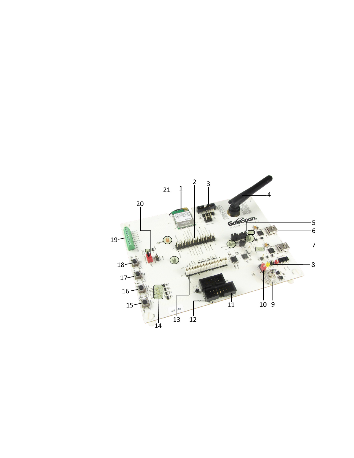
1.1.1 GS2011M Module Evaluation Board
Figure 1, page 19 illustrates key components included on the GS2011M evaluation board.
The evaluation board supports GS2011M module and provides access to SDIO, SPI,
UART, and GPIO interfaces. The evaluation board includes temperature and light sensors,
USB interfaces, power jumpers for power measurement, a daughter board header, and
buttons for various features. Table 6, page 20 lists the evaluation board components on the
GS2011M EVB 2.0. Table 7, page 22 lists the evaluation board components on the
GS2011M EVB 3.0.
Figure 1 GS2011M Evaluation Board Components
1VV0301435 Rev. 1.5 19 2018-12-11
Page 20

GS2K Module Evaluation Board Hardware User Guide
Table 6 GS2011M Module Evaluation Board Components - EVB 2.0
No. Feature Description
1 RF Module GS2011M
2 Daughter Board Header (J1) Header to facilitate connection to a daughter board
3
Test Points (TP1, TP5, TP6,
TP7, and TP17)
4 ANT2 Antenna used to communicate
5
Power Measurement Jumpers
(J11, J14, J15, and J16)
6 I/O Port (J6) Mini USB Connector (USB0)
7 I/O Port (J10) Mini USB Connector (USB1)
8
Test Points (TP2, TP3, and
TP16)
9 On/Off Switch (SW6) Power ON/OFF switch
10 Power Jumpers (J30, J31, J32)
11 SDIO Connector (J20) Secure Digital Input/Output connector
12 SPI Connector (J19) Serial connector
Test points for connecting VPP, Active, Deep Sleep,
Standby, and Ground (see Appendix B Connector
Pinouts, page 68 for more information on test point and
description)
Jumpers to facilitate measurement of current
consumption of module, (see Appendix A GS2000
Evaluation Board Specifications, page 50 for more
information on jumper settings and description)
Test points for connecting external power supply (see
Appendix B Connector Pinouts, page 68 for more
information on test point and description)
See Appendix A GS2000 Evaluation Board
Specifications, page 50 for more information on jumper
settings and description
If installed (default), these jumpers enable LEDs (see
13 LED Select Jumper (J4)
Appendix A GS2000 Evaluation Board Specifications,
page 50 for more information on jumper settings and
description)
Status LEDs (see Appendix A GS2000 Evaluation
14 LEDs
Board Specifications, page 50 for more information on
jumper settings and description)
15 Alarm Switch (SW3, SW4) Push button switch for Alarm 1 and Alarm 2
16 WPS Switch (SW1) Push button switch to enter WPS mode (not used)
17 Restore Switch (SW2)
Push button switch to restore the board to factory default
settings (not used)
18 Reset Switch (SW7) Push button switch to reset the GS2011M
19 Light Sensor (Q10)
20 Temperature Sensor (RT1)
Used to detect and read light sensor data when using the
TLS mobile application
Used to detect and read temperature sensor data when
using the TLS mobile application
1VV0301435 Rev. 1.5 20 2018-12-11
Page 21
GS2K Module Evaluation Board Hardware User Guide
Table 6 GS2011M Module Evaluation Board Components - EVB 2.0 (Continued)
No. Feature Description
21 Program Switch (SW5)
22 JTAG Connector (J21)
23 Test Point Header (J2)
NOTE: For GS2011M hardware specifications, refer to the GainSpan GS2011M
Wi-Fi Module Hardware User Guide.
RUN: Normal Operation (default)
PROGRAM: For programming the module
Used for testing and debugging the GS2011M
evaluation board
Additional module pins that don’t go to daughter board
header
1VV0301435 Rev. 1.5 21 2018-12-11
Page 22

GS2K Module Evaluation Board Hardware User Guide
Table 7 GS2011M Module Evaluation Board Components - EVB 3.0
No. Feature Description
1RF Module GS2011M
2 Daughter Board Header (J1)
3
Test Points (TP1, TP5, TP6,
TP7,and TP17)
4 ANT2 Antenna used to communicate
5
Power Measurement Jumpers
(J14 and J15)
6 I/O Port (J6) Mini USB Connector (USB0)
7 I/O Port (J10) Mini USB Connector (USB1)
Header to facilitate connection to a daughter
board
Test points for connecting VPP, Active, Deep
Sleep, Standby, and Ground (see Appendix B
Connector Pinouts, page 68 for more information
on test point and description)
Jumpers to facilitate measurement of current
consumption of module, (see Appendix A
GS2000 Evaluation Board Specifications,
page 50 for more information on jumper settings
and description)
Test points for connecting external power supply
8 Test Points (TP3 and TP16)
(see Appendix B Connector Pinouts, page 68 for
more information on test point and description)
9 On/Off Switch (SW6) Power ON/OFF switch
See Appendix A GS2000 Evaluation Board
10 Power Jumpers (J31, J32)
Specifications, page 50 for more information on
jumper settings and description
11 SDIO Connector (J20) Secure Digital Input/Output connector
12 SPI Connector (J19) Serial connector
If installed (default), these jumpers enable LEDs
13 LED Select Jumper (J4)
(see Appendix A GS2000 Evaluation Board
Specifications, page 50 for more information on
jumper settings and description)
Status LEDs (see Appendix A GS2000
14 LEDs
Evaluation Board Specifications, page 50 for
more information on jumper settings and
description)
15 Alarm Switch (SW3, SW4) Push button switch for Alarm 1 and Alarm 2
16 WPS Switch (SW1) Push button switch to enter WPS mode (not used)
17 Restore Switch (SW2)
Push button switch to restore the board to factory
default settings (not used)
18 Reset Switch (SW7) Push button switch to reset the GS2011M
19 Light Sensor (Q10)
1VV0301435 Rev. 1.5 22 2018-12-11
Used to detect and read light sensor data when
using the TLS mobile application
Page 23
GS2K Module Evaluation Board Hardware User Guide
Table 7 GS2011M Module Evaluation Board Components - EVB 3.0 (Continued)
No. Feature Description
20 Temperature Sensor (RT1)
21 Program Switch (SW8)
22 JTAG Connector (J21)
23 Test Point Header (J2)
Used to detect and read temperature sensor data
when using the TLS mobile application
RUN: Normal Operation (default)
PROGRAM: For programming the module
Used for testing and debugging the GS2011M
evaluation board
Additional module pins that don’t go to daughter
board header
1VV0301435 Rev. 1.5 23 2018-12-11
Page 24

GS2K Module Evaluation Board Hardware User Guide
1.2 GainSpan GS2100M Low Power 802.11b/g/n Module
The GS2100M module provides a quick, easy, and cost effective way for device and
appliance manufacturers to add Wi-Fi connectivity to their products. Intended for smart
energy and sensor applications, the module runs the SEP 2.0 Smart Energy Profile stack and
has 3 high bit-rate sigma-delta ADCs for high resolution sensor and measurement devices.
This module provides a UART/SPI/SDIO serial interface or Wi-Fi connectivity to
embedded design with an 8/16/32-bit micro controller. Alternatively, it can be run
self-contained without a host.
The GS2100M is an ideal solution for organizations with limited Wi-Fi or RF expertise or
for those seeking faster time to market, as it reduces RF design time and removes the burden
of testing and certification.
The module runs the full Wi-Fi and TCP/IP networking stacks, completely offloading the
host micro controller. It supports a complete suite of security protocols, also without
tasking the host micro controller, including WPA/WPA2-Enterprise and Personal security
modes, legacy WEP encryption, and upper layer security protocols such as TLS/SSL and
HTTPS. For ease of provisioning, the module can be set up simply and easily from a smart
phone or laptop through the innovative Limited AP mode or with Wi-Fi Protected Setup
(WPS 2.0).
The GainSpan GS2100M module is designed to support the following features:
– An on-board antenna or u.FL connector to add an external antenna for extended
range
– Full Wireless LAN and Network services offload solution minimizes load on host
processor
– Enables Smart Energy Profiles; Smart Thermostat and Load Control
– High resolution sensing and energy measurements
– Easy provisioning with Limited AP or Wi-Fi protected set up (WPS 2.0)
– Low power consumption through dynamic management modes: Standby, Sleep,
Deep Sleep
– IEEE 802.11 b/g/n connectivity
– UART, SPI, SDIO interface to micro controller
– Security: 802.11i, WPA/2-Personal and Enterprise, legacy WEP
The GainSpan module is easily designed into embedded systems, allowing customers to
develop a broad array of devices and appliances that connect to other local devices or the
Internet over Wi-Fi. Applications include smart energy, healthcare and fitness, industrial
controls, commercial building automation, and consumer electronics.
1VV0301435 Rev. 1.5 24 2018-12-11
Page 25
GS2K Module Evaluation Board Hardware User Guide
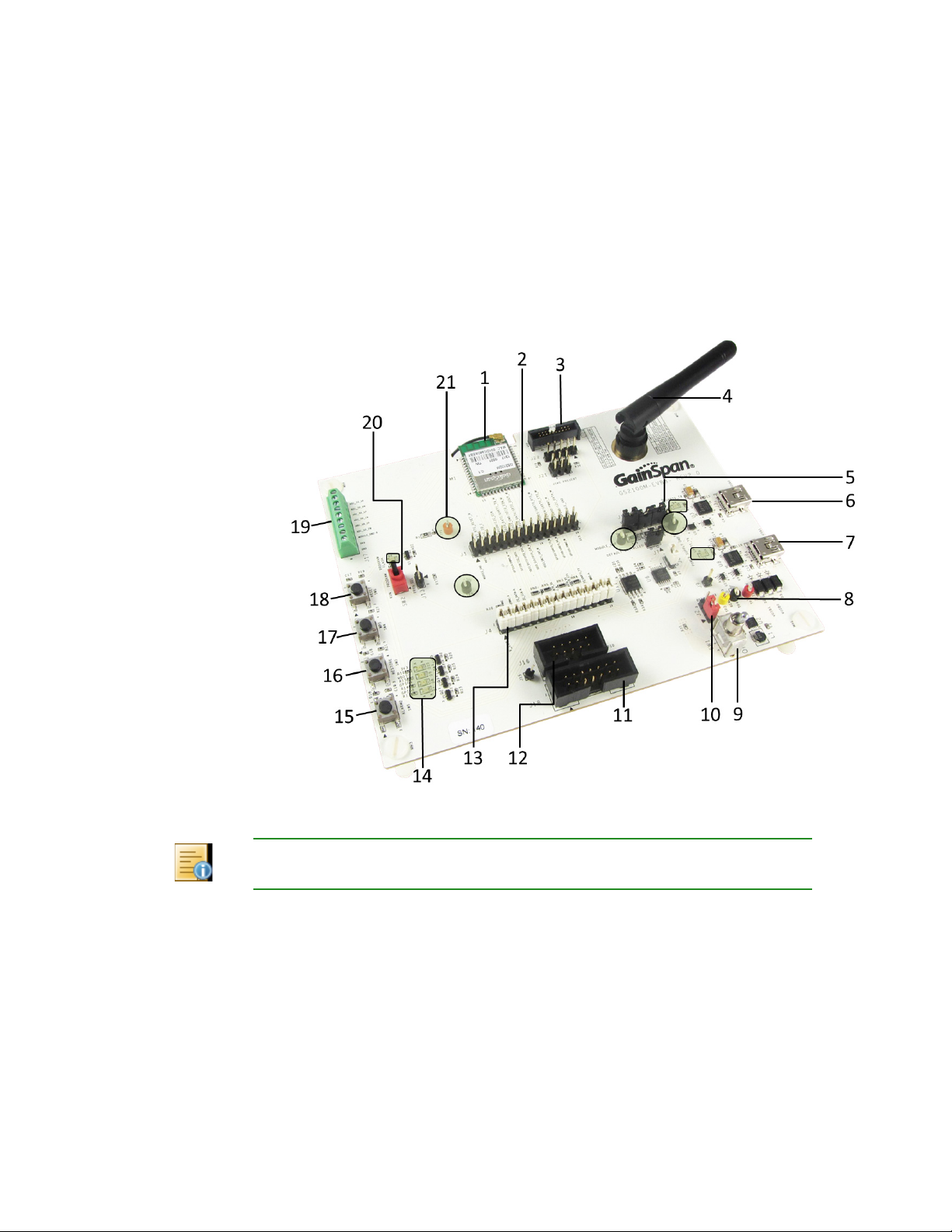
1.2.1 GS2100M Module Evaluation Board
Figure 2, page 25 illustrates key components included on the GS2100M evaluation board.
The evaluation board supports GS2100M module and provides access to SDIO, SPI,
UART, and GPIO interfaces. The evaluation board includes USB interfaces, power jumpers
for power measurement, a daughter board header, and buttons for various features. Tab le 8,
page 26 lists the evaluation board components on the GS2100M EVB 2.0. Table 9, page 28
lists the evaluation board components on the GS2100M EVB 3.0.
Figure 2 GS2100M Evaluation Board Components
NOTE: When using dual UART, connect GPIO30 to J9 for UART1RX to work
properly.
1VV0301435 Rev. 1.5 25 2018-12-11
Page 26

GS2K Module Evaluation Board Hardware User Guide
Table 8 GS2100M Module Evaluation Board Components - EVB 2.0
No. Feature Description
1 RF Module GS2100M
2 Daughter Board Header (J1) Header to facilitate connection to a daughter board
3 JTAG Connector (J19)
4 ANT1 Antenna used to communicate
5
Power Measurement Jumpers (J7,
J10, J11, and J12)
6 I/O Port (J6) Mini USB Connector (USB0)
7 I/O Port (J10) Mini USB Connector (USB1)
8 Test Points (TP2, TP3, and TP4)
Used for testing and debugging the GS2100M
evaluation board
Jumpers to facilitate measurement of current
consumption of module, (see Appendix A GS2000
Evaluation Board Specifications, page 50 for more
information on jumper settings and description)
Test points for connecting external power supply
(see Appendix B Connector Pinouts, page 68 for
more information on test point and description)
9 On/Off Switch (SW1) Power ON/OFF switch
See Appendix A GS2000 Evaluation Board
10 Power Jumper (J2)
Specifications, page 50 for more information on
jumper settings and description
11 SDIO Connector (J18) Secure Digital Input/Output connector
12 SPI Connector (J16) Serial Peripheral Interface connector
If installed (default), these jumpers enable LEDs (see
13 LED Select Jumper (J4)
Appendix A GS2000 Evaluation Board
Specifications, page 50 for more information on
jumper settings and description)
Status LEDs (see Appendix A GS2000 Evaluation
14 LEDs
Board Specifications, page 50 for more information
on jumper settings and description)
15 Alarm Switch (SW5) Push button switch for Alarm 2
16 Restore Switch (SW4)
Push button switch to restore the board to factory
default settings (not used)
17 WPS Switch (SW3) Push button switch to enter WPS mode (not used)
18 Reset Switch (SW6) Push button switch to reset the GS2100M
1VV0301435 Rev. 1.5 26 2018-12-11
Page 27
GS2K Module Evaluation Board Hardware User Guide
Table 8 GS2100M Module Evaluation Board Components - EVB 2.0 (Continued)
No. Feature Description
19
Analog to Digital Converter
(ADC) Connector (J17)
20 Program Switch (SW2)
21
Test Points (TP1, TP5, TP6, TP7,
and TP8)
NOTE: For GS2100M hardware specifications, refer to the GainSpan GS2100M
Wi-Fi Module Hardware User Guide.
A 3 high bit-rate Sigma Delta ADC connector for
high resolution sensor and measurement devices
RUN: Normal Operation (default)
PROGRAM: For programming the module
Test points for connecting VPP, Active, Deep Sleep,
Standby, and Ground (see Appendix B Connector
Pinouts, page 68 for more information on test point
and description)
1VV0301435 Rev. 1.5 27 2018-12-11
Page 28

GS2K Module Evaluation Board Hardware User Guide
Table 9 GS2100M Module Evaluation Board Components - EVB 3.0
No. Feature Description
1 RF Module GS2100M
2 Daughter Board Header (J1)
3 JTAG Connector (J19)
4 ANT1 Antenna used to communicate
5
Power Measurement Jumpers (J10, J11,
and J12)
6 I/O Port (J3) Mini USB Connector (USB0)
7 I/O Port (J8) Mini USB Connector (USB1)
8 Test Points (TP3 and TP4)
9 On/Off Switch (SW1) Power ON/OFF switch
10 Power Jumper (J2)
11 SDIO Connector (J18) Secure Digital Input/Output connector
12 SPI Connector (J16) Serial Peripheral Interface connector
Header to facilitate connection to a daughter
board
Used for testing and debugging the GS2100M
evaluation board
Jumpers to facilitate measurement of current
consumption of module, (see Appendix A
GS2000 Evaluation Board Specifications,
page 50 for more information on jumper settings
and description)
Test points for connecting external power supply
(see Appendix B Connector Pinouts, page 68 for
more information on test point and description)
See Appendix A GS2000 Evaluation Board
Specifications, page 50 for more information on
jumper settings and description
If installed (default), these jumpers enable LEDs
13 LED Select Jumper (J4)
(see Appendix A GS2000 Evaluation Board
Specifications, page 50 for more information on
jumper settings and description)
Status LEDs (see Appendix A GS2000
14 LEDs
Evaluation Board Specifications, page 50 for
more information on jumper settings and
description)
15 Alarm Switch (SW5) Push button switch for Alarm 2
16 Restore Switch (SW4)
17 WPS Switch (SW3)
Push button switch to restore the board to factory
default settings (not used)
Push button switch to enter WPS mode (not
used)
18 Reset Switch (SW6) Push button switch to reset the GS2100M
1VV0301435 Rev. 1.5 28 2018-12-11
Page 29

GS2K Module Evaluation Board Hardware User Guide
Table 9 GS2100M Module Evaluation Board Components - EVB 3.0 (Continued)
No. Feature Description
Analog to Digital Converter (ADC)
19
Connector (J17)
Analog to Digital Converter (ADC)
Header (J26)
20 Program Switch (SW7)
21
Test Points (TP1, TP5, TP6, TP7, and
TP8)
A 3 high bit-rate Sigma Delta ADC connector
and header for high resolution sensor and
measurement devices
RUN: Normal Operation (default)
PROGRAM: For programming the module
Test points for connecting VPP, Active, Deep
Sleep, Standby, and Ground (see Appendix B
Connector Pinouts, page 68 for more
information on test point and description)
1VV0301435 Rev. 1.5 29 2018-12-11
Page 30

GS2K Module Evaluation Board Hardware User Guide
1.3 GainSpan GS2101M Ultra-Low Power 802.11b/g/n Module
The GS2101M based modules provide cost effective, low power, and flexible platform to
add Wi-Fi® connectivity for embedded devices for a variety of applications, such as
wireless sensors and thermostats. It uses the GS2000 SoC, which combines ARM® Cortex
M3-based processors with a 802.11b/g/n Radio, MAC, security, & PHY functions, RTC
and SRAM, up to 4 MB FLASH, and on-board with an OFF module certified antenna
options. The module provides a Wi-Fi and regulatory certified IEEE 802.11b/g/n radio with
concurrent network processing services for a variety of app lications along with the existing
802.11 wireless network infrastructures.
The GS2101M is an ideal solution for organizations with limited Wi-Fi/RF expertise or for
those seeking faster time to market, as it reduces RF design time and removes the load of
testing and certification.
The module runs the full Wi-Fi and TCP/IP networking stacks, completely offloading the
host micro controller. It supports a complete suite of security protocols, also without
tasking the host micro controller, including WPA/WPA2-Enterprise and Personal security
modes, legacy WEP encryption, and upper layer security protocols such as TLS/SSL and
HTTPS. For ease of provisioning, the module can be set up simply and easily from a smart
phone or laptop through the innovative Limited AP mode or with Wi-Fi Protected Setup
(WPS 2.0).
The GainSpan GS2101M module is designed to support the following features:
– An on-board PCB trace antenna/u.FL connector to add an external antenna for
extended range.
– Full Wireless LAN and Network services offload solution minimizes load on host
processor.
– Enables Smart Energy Profiles; Smart Thermostat and Load Control.
– High resolution sensing and energy measurements.
– Easy provisioning with Limited AP or Wi-Fi protected set up (WPS 2.0).
– Low power consumption through dynamic management modes: Standby, Sleep,
Deep Sleep.
– IEEE 802.11 b/g/n connectivity.
– UART, SPI, SDIO interface to micro controller.
– Security: 802.11i, WPA/2-Personal and Enterprise, legacy WEP.
The GainSpan module is easily designed into embedded systems, allowing customers to
develop a broad array of devices and appliances that connect to other local devices/ Internet
over Wi-Fi. Applications include smart energy, healthcare and fitness, industrial
controls, commercial building automation, and consumer electronics.
1VV0301435 Rev. 1.5 30 2018-12-11
Page 31

GS2K Module Evaluation Board Hardware User Guide
1.3.1 GS2101M Module Evaluation Board
Figure 3, page 31 illustrates key components included on the GS2101M evaluation board.
The evaluation board supports GS2101M module and provides access to SDIO, SPI,
UART, and GPIO interfaces. The evaluation board includes USB interfaces, power jumpers
for power measurement, a daughter board header, and buttons for various features. Tab l e
10, page 31 lists the evaluation board components on the GS2101M EVB 3.1.
Figure 3 GS2101M Evaluation Board Components
NOTE: When using dual UART, connect GPIO30 to J9 for UART1RX to work
properly.
Table 10 GS2101M Module Evaluation Board Components - EVB 3.1
No. Feature Description
1 RF Module GS2101M
2 Daughter Board Header (J1) Header to facilitate connection to a daughter board
3 JTAG Connector (J19)
Used for testing and debugging the GS2101M
evaluation board
4 ANT1 Antenna used to communicate
1VV0301435 Rev. 1.5 31 2018-12-11
Page 32

GS2K Module Evaluation Board Hardware User Guide
Table 10 GS2101M Module Evaluation Board Components - EVB 3.1 (Continued)
No. Feature Description
5
Power Measurement Jumpers
(J10, J11, and J12)
6 I/O Port (J3) Mini USB Connector (USB0)
7 I/O Port (J8) Mini USB Connector (USB1)
8 Test Points (TP3, and TP4)
9 On/Off Switch (SW1) Power ON/OFF switch
10 Power Jumper (J2)
11 SDIO Connector (J18) Secure Digital Input/Output connector
12 SPI Connector (J16) Serial Peripheral Interface connector
Jumpers to facilitate measurement of current
consumption of module, (see Appendix A GS2000
Evaluation Board Specifications, page 50 for more
information on jumper settings and description)
Test points for connecting external power supply
(see Appendix B Connector Pinouts, page 68 for
more information on test point and description)
See Appendix A GS2000 Evaluation Board
Specifications, page 50 for more information on
jumper settings and description
If installed (default), these jumpers enable LEDs (see
13 LED Select Jumper (J4)
Appendix A GS2000 Evaluation Board
Specifications, page 50 for more information on
jumper settings and description)
Status LEDs (see Appendix A GS2000 Evaluation
14 LEDs
Board Specifications, page 50 for more information
on jumper settings and description)
15 Alarm Switch (SW5) Push button switch for Alarm 2
16 Restore Switch (SW4)
Push button switch to restore the board to factory
default settings (not used)
17 WPS Switch (SW3) Push button switch to enter WPS mode (not used)
18 Reset Switch (SW6) Push button switch to reset the GS2101M
Analog to Digital Converter
19
(ADC) Connector (J17) and
Analog to Digital Converter
A 3 high bit-rate Sigma Delta ADC connector for
high resolution sensor and measurement devices
(ADC) Connector (J26)
20 Program Switch (SW7)
RUN: Normal Operation (default)
PROGRAM: For programming the module
Test points for connecting VPP, Active, Deep Sleep,
21
Test Points (TP1, TP5, TP6, TP7,
and TP8)
Standby, and Ground (see Appendix B Connector
Pinouts, page 68 for more information on test point
and description)
1VV0301435 Rev. 1.5 32 2018-12-11
Page 33

GS2K Module Evaluation Board Hardware User Guide
NOTE: For GS2101M hardware specifications, refer to the GainSpan GS2101M
Low Power Wi-Fi Module Hardware User Guide.
1VV0301435 Rev. 1.5 33 2018-12-11
Page 34

GS2K Module Evaluation Board Hardware User Guide
1.4 GainSpan GS2200M Ultra-Low Power 802.11b/g/n Module
The GS2200M module provides a quick, easy, and cost effective way for device and
appliance manufacturers to add Wi-Fi connectivity to their products. The module provides
a built-in application CPU to run the device's application firmware on the module,
eliminating the need for an external host MCU. Alternatively, the module can be interfaced
with a host MCU via a UART, SPI or SDIO interface.
The GS2200M module supports ultra-low power mode enabling designs for both battery
powered or line powered applications. Alternatively, it can be run self-contained without a
host (to develop a hostless application an SDK is required). GS2200M is an ideal solution
for organizations with limited Wi-Fi/RF expertise and for those seeking faster time to
market, as it reduces RF design time and the load of testing and certification. The module
incorporates a complete Wi-Fi and TCP/IP networking stack, a full suite of networking
service includes Wi-Fi provisioning, DHCP, TLS/SSL, HTTP(S), mDNS, DNS, CoAP,
XML, JSON and Over-the-Air firmware upgrade.
GainSpan module is easily designed into an embedded system by allowing the user to
develop a broad array of devices and appliances that connect to other local devices/Internet
over Wi-Fi.
Example: Smart energy, healthcare and fitness, industrial controls, commercial building
automation, and consumer electronics.
The GainSpan GS2200M module is designed to support the following features:
– An on-board antenna or u.FL connector to add an external antenna for extended
range.
– Wireless LAN and network service offload solution minimizes load on host
processor.
– Ultra low power consumption through dynamic management modes: Standby,
Sleep, Deep Sleep.
– Easy provisioning with Limited AP or Wi-Fi protected set up (WPS 2.0).
– IEEE 802.11 b/g/n connectivity.
– UART, SPI, SDIO interface to peripherals or a host MCU.
– Security: 802.11i, WPA/2-Personal and Enterprise, legacy WEP, TLS.
1.4.1 GS2200M Module Evaluation Board
Figure 4, page 35 illustrates key components included on the GS2200M evaluation board.
The evaluation board supports GS2200M module and provides access to SDIO, SPI,
UART, and GPIO interfaces. The evaluation board includes USB interfaces, power jumpers
for power measurement, a daughter board header, and buttons for various features. Tab l e
11, page 35 lists the evaluation board components on the GS2200M EVB 1.1.
1VV0301435 Rev. 1.5 34 2018-12-11
Page 35

GS2K Module Evaluation Board Hardware User Guide
Figure 4 GS2200M Evaluation Board Components
Table 11 GS2200M Module Evaluation Board Components - EVB 1.1
No. Feature Description
1 RF Module GS2200M
2 Daughter Board Header (J1) Header to facilitate connection to a daughter board
3 JTAG Connector (J21)
Used for testing and debugging the GS2200M
evaluation board.
4 ANT2 Antenna used to communicate
Jumpers to facilitate measurement of current
5
Power Measurement Jumpers
(J11 and J14)
consumption of module, (see Appendix A GS2000
Evaluation Board Specifications, page 50 for more
information on jumper settings and description)
6 I/O Port (J6) Mini USB Connector (USB0)
7 I/O Port (J10) Mini USB Connector (USB1)
8
Test Points (TP2, TP3, and
TP16)
Test points for connecting external power supply (see
Appendix B Connector Pinouts, page 68 for more
information on test point and description)
9 On/Off Switch (SW6) Power ON/OFF switch
1VV0301435 Rev. 1.5 35 2018-12-11
Page 36

GS2K Module Evaluation Board Hardware User Guide
Table 11 GS2200M Module Evaluation Board Components - EVB 1.1 (Continued)
No. Feature Description
10 Power Jumpers (J31)
11 SDIO Connector (J20) Secure Digital Input/Output connector
12 SPI Connector (J19) Serial connector
13 LED Select Jumper (J4)
14 LEDs
15 Alarm Switch (SW3, SW4) Push button switch for Alarm 2
See Appendix A GS2000 Evaluation Board
Specifications, page 50 for more information on jumper
settings and description
If installed (default), these jumpers enable LEDs (see
Appendix A GS2000 Evaluation Board Specifications,
page 50 for more information on jumper settings and
description)
Status LEDs (see Appendix A GS2000 Evaluation
Board Specifications, page 50 for more information on
jumper settings and description)
16 Restore Switch (SW2)
Push button switch to restore the board to factory default
settings (not used)
17 WPS Switch (SW1) Push button switch to enter WPS mode (not used)
18 Reset Switch (SW7) Push button switch to reset the GS2200M
A single high bit-rate Sigma Delta ADC and single SAR
ADC connector for high resolution sensor and
measurement devices.
19
Analog to Digital Converter
(ADC) Header (J2)
RUN: Normal Operation (default)
20 Program Switch (SW8)
PROGRAM: For programming the module
Test points for connecting VPP, Active, Deep Sleep,
21
Test Point (TP1, TP5, TP6, TP7
and TP17)
Standby, and Ground (see Appendix B Connector
Pinouts, page 68 for more information on test point and
description)
NOTE: For GS2200M hardware specifications, refer to the GainSpan GS2200M
Low Power Wi-Fi Module Hardware User Guide.
1VV0301435 Rev. 1.5 36 2018-12-11
Page 37

GS2K Module Evaluation Board Hardware User Guide
1.5 Evaluation Board Software
The evaluation board ships with Serial-to-Wi-Fi firmware, which uses the UART interface
at 9600 Baud, 8-bit (8), No parity bit (N), one stop bit (1) that abstracts the hardware and
provides Wireless LAN (WLAN) and Network Services for embedded applications.
NOTE: To use other I/O interfaces for Serial-to-Wi-Fi, such as SPI, or to
customize firmware features you can build the binaries using the SDK Builder and
reprogram the module using the gs2k_flashprogram utility. If using Serial-to-Wi-Fi
with SPI, you will need to wire the host to the SPI0 connector or use the daughter
board connector. Refer to the GS2011M or GS2100M or GS2200M or GS2101M
evaluation board schematic for connections.
To evaluate a hostless application such as Temperature and Light Sensor (TLS), refer to the
GainSpan Temperature and Light Sensor (TLS) Demo Application Note.
NOTE: Additional software/documentation are available on the Telit Wi-Fi
Support Portal website: https://wifi.telit.com/secure/login
NOTE: For re-programming the module, use the gs2k_flashprogram GUI tool
and follow the steps per the GainSpan GS2000 Based Module Programming User
Guide.
NOTE: The Temperature and Light Sensor (TLS) application is supported on the
GS2011M and GS2200M evaluation board only.
1VV0301435 Rev. 1.5 37 2018-12-11
Page 38

GS2K Module Evaluation Board Hardware User Guide
Chapter 2 Setting Up the Evaluation Board
This chapter introduces the tasks that are typically required to setting up the GainSpan®
GS2000 based module evaluation board for GS2011M, GS2100M, GS2200M and
GS2101M. You can begin the setup process as soon as the site preparation is complete and
the board is unpacked and inspected.
Refer to Appendix A GS2000 Evaluation Board Specifications, page 50 in this manual
regarding electrical and environmental requirements.
The following sections are covered in this chapter:
• Preparing for Evaluation Board Setup, page 38
• Setting Up the GS2000 Based Module Evaluation Board, page 41
• Power Guidelines, Requirements, and Safety Specifications, page42
2.1 Preparing for Evaluation Board Setup
This section describes how to prepare for setting up the GS2000 based module evaluation
board. It discusses the following topics:
• Site Preparation, page 39
• Safety Guidelines and Standards, page 39
• Environmental Requirements, page 39
• Unpacking and Inspecting the GS2000 Based Module Evaluation Board, page 40
• Placing the GS2000 Based Module Evaluation Board on a Tabletop, page 41
• Electrical Guidelines, page 42
• Connecting Power, page 42
1VV0301435 Rev. 1.5 38 2018-12-11
Page 39

GS2K Module Evaluation Board Hardware User Guide
2.1.1 Site Preparation
The following table (Table 12, page 39) summarizes the tasks you need to perform when
preparing to setup your GS2000 based module evaluation board.
Item and/or Task Notes
Verify that the environmental factors such
as temperature and humidity do not exceed
required tolerances
Plan evaluation board location
Acquire cables
Download product documentation
2.1.2 Safety Guidelines and Standards
To ensure that you setup the evaluation board safely, observe the following guidelines:
Table 12 Setup Checklist
• Review the information in Appendix A GS2000 Evaluation Board Specifications,
page 50 and observe all safety information and precautions and warnings
provided throughout this manual.
• Comply with all applicable safety requirements, practices, and standards. Refer to
Appendix A GS2000 Evaluation Board Specifications, page 50.
• After setting up the evaluation board, protect your equipment by using an ESD
approved grounding strap whenever handling board components.
2.1.3 Environmental Requirements
The following Environmental Requirements must be taken into consideration when setting
up the evaluation board. Specific details and values for following key environmental
requirements are listed in Table 13, page 51, Table 18, page 56, Table 26, page 64 and Table
22, page 60.
1VV0301435 Rev. 1.5 39 2018-12-11
Page 40

GS2K Module Evaluation Board Hardware User Guide
2.1.4 Unpacking and Inspecting the GS2000 Based Module Evaluation Board
This section describes how to remove the evaluation board from its shipping box, and
determine that you received all of the required equipment.
The unpacking process is described in the following steps:
1. Remove the packing slip from the shipping box. Use this paper work to validate the
contents.
2. Prepare to remove the evaluation board from the shipping box.
• Remove cabling from the box and set it aside
• Remove any documentation from the box and set it aside
3. Carefully lift the evaluation board from the shipping container.
4. Remove the protective ESD bag from the evaluation board.
5. Set all protective packaging aside for later use.
6. Inspect the contents for damage.
If damaged, contact your GainSpan distributor to file a RMA (see Returning Products to
Telit, page 16).
1VV0301435 Rev. 1.5 40 2018-12-11
Page 41

GS2K Module Evaluation Board Hardware User Guide
2.2 Setting Up the GS2000 Based Module Evaluation Board
This section describes how to perform the following installation tasks:
• Place the evaluation board on a secure flat surface
• Connect all cabling
• Apply and verify power to the evaluation board
2.2.1 Placing the GS2000 Based Module Evaluation Board on a Tabletop
The evaluation board must be set on a sturdy tabletop or workbench environment. Use safe
practices when placing evaluation boards next to each other.
1VV0301435 Rev. 1.5 41 2018-12-11
Page 42

GS2K Module Evaluation Board Hardware User Guide
2.3 Power Guidelines, Requirements, and Safety Specifications
The following sections contain important safety, planning, and power requirements
information.
2.3.1 Electrical Guidelines
When connecting power to the evaluation board, observe all caution and warning
statements. The following guidelines will help ensure your safety and protect the
equipment. However, these guidelines may not cover all potentially hazardous situations
you may encounter during board installation.
• Always disconnect all cables before installing
• Keep the evaluation board area clear and free of dust during and after installation
• The evaluation board operates safely when it is used in accordance with its
marked electrical ratings and product usage instructions.
WARNING! Before connecting or re-connecting header and test point cabling,
turn the power switch off and disconnect the mini-USB cable from the board.
2.3.2 Connecting Power
The evaluation board gets power from a computer USB port via the mini-USB cable.
The board is designed to operate on only one USB connection. Power can also be supplied
from the USB1 port or a 3.3V Bench Supply to TP3 (Yellow).
ESD ALERT! Charged devices and circuit boards can discharge without
detection. Although this product features patented or protection circuitry, damage
may occur on devices subjected to high energy. Therefore, proper ESD
precautions should be taken to avoid performance degradation or loss of
functionality.
1VV0301435 Rev. 1.5 42 2018-12-11
Page 43

GS2K Module Evaluation Board Hardware User Guide
Chapter 3 Initial Board Connections and Configuration
This chapter describes how to quickly administer initial settings and start a Serial-to-Wi-Fi
application on a GainSpan
The following sections are covered in this chapter:
• Connecting the Board to a Communication Port, page 43
• Providing Power to the Evaluation Board, page 46
• Configuring the Board for Wireless Network, page 48
®
GS2000 based module evaluation board.
3.1 Connecting the Board to a Communication Port
There are a few basic connections that must be addressed in order to communicate with the
GS2000 based module evaluation board.
Perform the following:
1. Plug the mini-USB cable into the USB0 port on the evaluation board, and plug the
other end of the mini-USB cable into the USB port on a computer.
2. From the Windows desktop, open the Device Manager as shown in Figure 5, page 43.
The USB Serial port is listed under Ports (COM & LPT).
Figure 5 Windows Device Manager Properties
1VV0301435 Rev. 1.5 43 2018-12-11
Page 44

GS2K Module Evaluation Board Hardware User Guide
NOTE: The FTDI Virtual COM port driver can enumerate devices to any one of a
number of COM ports. It is necessary to find the COM port being used to
communicate with the GS2000 based module evaluation board.
3. Open the GS2000 software release folder, and unzip the files to a location on your C:\
drive.
4. Under the SW Utilities folder, select the Tera Term VT terminal emulation application
(teraterm_utf8-4.58 or later) to install.
5. Open the Tera Term VT from your desktop and select the serial port associated with
the evaluation board (see Figure 6, page 44).
NOTE: The Serial Port must match the port identified.
Figure 6 Connect Evaluation Board to a Serial Port
1VV0301435 Rev. 1.5 44 2018-12-11
Page 45

GS2K Module Evaluation Board Hardware User Guide
6. Setup the Serial Port (COM port) as shown in Figure 7, page 45.
Figure 7 Select Serial Port (COM port) Settings
NOTE: For Temperature and Light Sensor (TLS) application set the Baud Rate to
115200.
1VV0301435 Rev. 1.5 45 2018-12-11
Page 46

GS2K Module Evaluation Board Hardware User Guide
3.2 Providing Power to the Evaluation Board
To provide power to the GS2000 based module evaluation board perform the following
procedures:
• Connect power to the evaluation board
3.2.1 Connecting Power to the Board
1. Plug the mini-USB cable into the USB0 port on the evaluation board and plug the
other end of the mini-USB cable into a USB port on a computer.
2. Turn the PROGRAM/RUN switch to the RUN position.
3. Turn the ON/OFF switch to the ON position.
4. The Serial2Wi-Fi APP ready prompt will display within the Tera Term VT window
(see Figure 8, page 46).
Figure 8 Serial-to-Wi-Fi Application Ready
5. Enter a basic AT command.
AT+VER=?
1VV0301435 Rev. 1.5 46 2018-12-11
Page 47

GS2K Module Evaluation Board Hardware User Guide
6. This command will respond back with the Serial-to-Wi-Fi firmware version (see
Figure 9, page 47).
Figure 9 Serial-to-Wi-Fi Firmware Version
7. Setup an Access Point (AP) that is specific to your environment and network.
1VV0301435 Rev. 1.5 47 2018-12-11
Page 48

GS2K Module Evaluation Board Hardware User Guide
3.3 Configuring the Board for Wireless Network
This section describes how to configure network settings on the GS2000 based module
evaluation board for the first time.
When configuring the evaluation board for the first time, make sure you have completed
the setup according to the hardware setup instructions in Chapter 2 Setting Up the
Evaluation Board, page 38. Before you setup the board, make sure you are using a
computer connected to the same network as the board, and obtain the correct serial
communication port information.
3.3.1 Connect to a Network
To begin connecting the GS2000 based module evaluation board to a network, use the AT
command, by connecting a computer or laptop with a terminal emulation program.
To look for available wireless networks, perform the following:
1. Enable DHCP by issuing the command.
AT+NDHCP=1
2. Scan for available Wi-Fi access points within your network by issuing the command.
AT+WS
3. Enter the SSID associated with the access point and channel number (optional).
AT+WA=<SSID>
The evaluation board will receive an IP address from the access point DHCP server.
1VV0301435 Rev. 1.5 48 2018-12-11
Page 49

GS2K Module Evaluation Board Hardware User Guide
The IP address, subnet, and gateway of the GainSpan node will be displayed upon
successful association (see Figure 10, page 49).
Figure 10 Receiving IP Address from the Access Point DHCP Server
For more information on how to setup application examples for:
• UDP and TCP client/server connections either in station (infrastructure mode) or
Limited AP mode.
• Demonstrate Temperature and Light Sensor (TLS) mobile application on iOS and
Android devices.
• Web Provisioning using Limited AP Provision mode and Wi-Fi Protected Setup
(WPS).
Refer to the Temperature and Light Sensor (TLS) Demo Application Note.
1VV0301435 Rev. 1.5 49 2018-12-11
Page 50

GS2K Module Evaluation Board Hardware User Guide
Appendix A GS2000 Evaluation Board Specifications
This appendix summarizes the physical, electrical, environmental specifications, on-board
jumper and switch settings for the GainSpan
GS2101M evaluation boards.
The following sections are covered in this appendix:
• GS2011M Evaluation Board Specifications, page 50
• GS2011M Evaluation Board LEDs, page 51
• GS2011M Evaluation Board Sensors, page 53
• GS2011M Evaluation Board Switches, page 53
• GS2011M Evaluation Board Jumper Settings, page 54
• GS2100M Evaluation Board Specifications, page 56
• GS2100M Evaluation Board LEDs, page 57
• GS2100M Evaluation Board Switches, page 58
• GS2100M Evaluation Board Jumper Settings, page 59
• GS2101M Evaluation Board Specifications, page 60
• GS2101M Evaluation Board LEDs, page 61
• GS2101M Evaluation Board Switches, page 62
®
GS2011M, GS2100M, GS2200M and
• GS2101M Evaluation Board Jumper Settings, page 63
• GS2200M Evaluation Board Specifications, page 64
• GS2200M Evaluation Board LEDs, page 65
• GS2200M Evaluation Board Sensors, page 66
• GS2200M Evaluation Board Switches, page 66
• GS2200M Evaluation Board Jumper Settings, page 67
A.1 GS2011M Evaluation Board Specifications
Table 13, page 51 lists the GS2011M evaluation board specifications.
1VV0301435 Rev. 1.5 50 2018-12-11
Page 51

GS2K Module Evaluation Board Hardware User Guide
Table 13 GS2011M Evaluation Board Specifications
Feature Description
Radio Protocol IEEE 802.11b/g/n
RF Operating Frequency 2.4 GHz
Supported Data Rates
Antenna External Antenna (u.FL connector) or On-board Antenna
Operating Temperature -40
Security Protocols
Networking Protocols
I/O Interfaces SPI, UART, SDIO, I
Host Connections SPI, UART, SDIO (typically to an external micro controller)
72, 65, 58, 43, 29, 22, 14, 7 Mbps (802.11n), 54, 48, 36, 24,
18, 12, 9, 6 Mbps (802.11g) 11, 5.5, 2, 1 Mbps (802.11b)
o
C to +85oC
WPA/WPA2 - Personal, WPA/WPA1 - Enterprise (PEAP,
EAP-FAST, EAP-TLS, EAP-TTLS), WEP, TLS/SSL Client
and Server, HTTPS
TCP, UDP, IPv4, IPv6, TLS Client and Server, SNTP Client,
DHCP Client and Server v4, DHCP Client and Server v6,
DNS Client and Server, HTTP Client and Server, XML Parser
2
C, I2S, GPIO, ADC (12-bit), JTAG
Outline Dimensions 22.8mm x 32.5mm x 3.63mm (shield)
I/O Voltage 3.3V VDDIO
Operating Voltage 2.7-3.6V
NOTE: For complete GS2011M module specifications, refer to the GS2011M
Wi-Fi Module Hardware User Guide.
A.2 GS2011M Evaluation Board LEDs
Table 14, page 51 lists the GS2011M evaluation board LEDs.
Table 14 GS2011M Evaluation Board LEDs
LED State EVB 2.0 EVB 3.0 Description
VIN_3V3 - D8 VIN_3V3 - D8
Power
3V3 - D9 3V3 - D9
LED on board will be Solid GREEN
indicating board is ON and receiving
input voltage
LED on board will be Solid GREEN
indicating board is ON and receiving
power voltage
1VV0301435 Rev. 1.5 51 2018-12-11
Page 52

GS2K Module Evaluation Board Hardware User Guide
Table 14 GS2011M Evaluation Board LEDs
LED State EVB 2.0 EVB 3.0 Description
GPIO8 - D2 GPIO30 - D2
General Purpose
Input/Output
GPIO9 - D3 GPIO31 - D3
RUN/PROGRAM
FLASH
PROGRAM - D1 PROGRAM - D1
UART0 - D5 UART0 - D5
Universal
Asynchronous
Receiver/Transmitter
UART1 - D7 UART1 - D7
General Purpose LED’s controlled either
by Serial-to-Wi-Fi AT commands or by
TLS firmware
General Purpose LED’s controlled either
by Serial-to-Wi-Fi AT commands or by
TLS firmware
LED on board will be Solid RED when
the RUN/PROGRAM switch is set to
PROGRAM mode
LED on board will be Solid AMBER
indicating that the board is transmitting
through the USB0 port
LED on board will be Solid AMBER
indicating that the board is transmitting
through the USB1 port
1VV0301435 Rev. 1.5 52 2018-12-11
Page 53

GS2K Module Evaluation Board Hardware User Guide
A.3 GS2011M Evaluation Board Sensors
Table 15, page 53 lists the GS2011M evaluation board sensors.
Table 15 GS2011M Evaluation Board Sensors
Sensor State EVB 2.0 and EVB 3.0 Description
Used to detect and read light sensor data when
Light Sensor Q10
Temperature Sensor RT1
using the Temperature and Light Sensor (TLS)
mobile application
Used to detect and read temperature sensor data
when using the Temperature and Light Sensor
(TLS) mobile application
A.4 GS2011M Evaluation Board Switches
Table 16, page 53 lists the GS2011M evaluation board switches.
Table 16 GS2011M Evaluation Board Switches
Switch State EVB 2.0 EVB 3.0 Description
WPS SW1 SW1
Restore SW2 SW2
SW3 SW3 Push button for Alarm1
Alarm
SW4 SW4 Push button for Alarm2
Program Flash SW5 SW8
ON/OFF SW6 SW6
Reset SW7 SW7
Push button switch to enter WPS mode (not
supported at this time)
Push button switch to restore the board to
factory default settings
Toggle switch to set the board in RUN mode
(default)
Toggle switch to set the board in PROGRAM
mode to program the module
Toggle switch to power ON/OFF the GS2011M
evaluation board
Push button switch to reset the GS2011M
evaluation board
1VV0301435 Rev. 1.5 53 2018-12-11
Page 54

GS2K Module Evaluation Board Hardware User Guide
A.5 GS2011M Evaluation Board Jumper Settings
Table 17, page 54 lists the GS2011M evaluation board jumper settings.
Table 17 GS2011M Evaluation Board Jumper Settings
Jumper State Jumpers on
EVB 2.0
J3 (default not
JTAG Header
LED Select
(all jumpers
installed-default)
installed) for
TRACE
connector J22
J4 - D1
J4 - D2
J4 - D3
J4 - D8
J4 - D9
Description Jumpers on
If JTAG is present, install
jumpers on pins 1-2 and 3-4. If
new JTAG install jumper on
pins 5-6. See GS2011M,
GS2100M, GS2101M and
GS2200M JTAG Cortex Debug
Connector Pinouts, page 68.
Install jumper enables LED for
Program Flash
Install jumper enables LED for
GPIO8
Install jumper enables LED for
GPIO9
Install jumper enables LED for
VDDIO (turns OFF in Standby
mode)
Install jumper enables LED for
3V3 (turns ON in Standby
mode)
EVB 3.0
No Jumper
connector
present
J4 - D1
J4 - D2
J4 - D3
J4 - D8
J4 - D9
Description
See GS2011M, GS2100M,
GS2101M and GS2200M JTAG
Cortex Debug Connector
Pinouts, page 68.
Install jumper enables LED for
Program Flash
Install jumper enables LED for
GPIO30
Install jumper enables LED for
GPIO31
Install jumper enables LED for
VDDIO (turns OFF in Standby
mode)
Install jumper enables LED for
3V3 (turns ON in Standby
mode)
J11 Installed (default) N/A N/A
J14 Active mode (default installed) J14 Active mode (default installed)
Power
Measurement
UART0 J29
Power
J15
J16
J30 Setting 3.3V or 1.8V N/A N/A
J31
J32
Deep Sleep mode (default
installed)
Standby mode (default
installed)
Install jumper on pins 1-2
(default installed)
Install jumper on pins 1-2:
Regulated 3.3V via on board
voltage regulator
Install jumper on pins 2-3:
External 3.3V bench supply
Install jumper on pins 2-3:
Standby Mode (default)
J15
N/A N/A
J29
J31
J32
Deep Sleep mode (default
installed)
Install jumper on pins 1-2
(default installed)
Install jumper on pins 1-2:
Regulated 3.3V via on board
voltage regulator
Install jumper on pins 2-3:
External 3.3V bench supply
Install jumper on pins 2-3:
Standby Mode (default)
1VV0301435 Rev. 1.5 54 2018-12-11
Page 55

GS2K Module Evaluation Board Hardware User Guide
Table 17 GS2011M Evaluation Board Jumper Settings (Continued)
Jumper State Jumpers on
Description Jumpers on
EVB 2.0
GPIO8 N/A N/A J24
GPIO9 N/A N/A J33
Note: Power is turned off to the board during Standby mode.
Description
EVB 3.0
Install jumper enables GPIO8
I2C Data
Install jumper enables GPIO9
I2C Clock
1VV0301435 Rev. 1.5 55 2018-12-11
Page 56

GS2K Module Evaluation Board Hardware User Guide
A.6 GS2100M Evaluation Board Specifications
Table 18, page 56 lists the GS2100M evaluation board specifications.
Table 18 GS2100M Evaluation Board Specifications
Feature Description
Radio Protocol IEEE 802.11b/g/n
RF Operating Frequency 2.4 GHz
Supported Data Rates
Antenna External Antenna (u.FLconnector) or Internal PCB Antenna
Operating Temperature -40
Security Protocols
Networking Protocols
I/O Interfaces SPI, UART, SDIO, I
72, 65, 58, 43, 29, 22, 14, 7 Mbps (802.11n), 54, 48, 36, 24, 18,
12, 9, 6 Mbps (802.11g) 11, 5.5, 2, 1 Mbps (802.11b)
o
C to +85oC
WPA/WPA2 - Personal, WPA/WPA2 - Enterprise (PEAP,
EAP-FAST, EAP-TLS, EAP-TTLS), WEP, TLS/SSL Client
and Server, HTTPS
TCP, UDP, IPv4, IPv6, TLS Client and Server, SNTP Client,
DHCP Client and Server v4, DHCP Client and Server v6, DNS
Client and Server, mDNS, DNS-SD, HTTP Client and Server,
XML Parser
2
C, GPIO, ADC (16-bit), JTAG
Host Connections SPI, UART, SDIO (typically to an external micro controller)
Outline Dimensions 18 mm x 25 mm x 2.5 mm (shield)
I/O Voltage 1.8V or 3.3V VDDIO
Operating Voltage 2.7-3.6V
NOTE: For complete GS2100M module specifications, refer to the GS2100M
Wi-Fi Module Data Sheet.
1VV0301435 Rev. 1.5 56 2018-12-11
Page 57

GS2K Module Evaluation Board Hardware User Guide
A.7 GS2100M Evaluation Board LEDs
Table 19, page 57 lists the GS2100M evaluation board LEDs.
Table 19 GS2100M Evaluation Board LEDs
LED State EVB 2.0 EVB 3.0 Description
LED on board will be Solid GREEN indicating
board is ON and receiving input voltage
LED on board will be Solid GREEN indicating
board is ON and receiving power voltage
General Purpose LED’s controlled either by
Serial-to-Wi-Fi AT commands or by TLS
firmware
General Purpose LED’s controlled either by
Serial-to-Wi-Fi AT commands or by TLS
firmware
LED on board will be Solid RED when the
RUN/PROGRAM switch is set to PROGRAM
mode
LED on board will be Solid AMBER indicating
that the board is transmitting through the USB0
port
LED on board will be Solid AMBER indicating
that the board is transmitting through the USB1
port
Power
General Purpose
Input/Output
RUN/PROGRAM
FLASH
Universal
Asynchronous
Receiver/Transmitter
VDDIO - D9 VDDIO - D9
3V3 - D10 3V3 - D10
GPIO8 - D7 GPIO30 - D7
GPIO9 - D8 GPIO31 - D8
PROGRAM - D6 PROGRAM - D6
UART0 - D5 UART0 - D4
UART1 - D7 UART1 - D5
1VV0301435 Rev. 1.5 57 2018-12-11
Page 58

GS2K Module Evaluation Board Hardware User Guide
A.8 GS2100M Evaluation Board Switches
Table 20, page 58 lists the GS2100M evaluation board switches.
Table 20 GS2100M Evaluation Board Switches
Switch State EVB 2.0 EVB 3.0 Description
WPS SW3 SW3
Restore SW4 SW4
Alarm SW5 SW5 Push button for Alarm2
Reset SW6 SW6 Resets to factory default (not available)
Program Flash SW2 SW7
Push button switch to enter WPS mode (not
supported at this time)
Push button switch to restore the board to factory
default settings
Toggle switch to set the board in RUN mode
(default)
Toggle switch to set the board in PROGRAM
mode to program the module
ON/OFF SW1 SW1
Toggle switch to power ON/OFF the GS2100M
evaluation board
1VV0301435 Rev. 1.5 58 2018-12-11
Page 59

GS2K Module Evaluation Board Hardware User Guide
A.9 GS2100M Evaluation Board Jumper Settings
Table 21, page 59 lists the GS2100M evaluation board jumper settings.
Table 21 GS2100M Evaluation Board Jumper Settings
Jumper State Jumpers on
EVB 2.0
J3 (default not
JTAG Header
LED Select (all
jumpers
installed-default)
installed) for
TRACE
connector J22
J4 - D1
J4 - D7
J4 - D8
J4 - D9
J4 - D10
Description Jumpers on
If JTAG is present, install
jumpers on pins 1-2 and 3-4. If
new JTAG, install jumper on pins
5-6. See GS2011M, GS2100M,
GS2101M and GS2200M JTAG
Cortex Debug Connector
Pinouts, page 68.
Install jumper enables LED for
Program Flash
Install jumper enables LED for
GPIO8
Install ju.mper enables LED for
GPIO9
Install jumper enables LED for
VDDIO (turns OFF in Standby
mode)
Install jumper enables LED for
3V3 (turns ON in Standby mode)
EVB 3.0
No Jumper
connector
present
J4 - D1
J4 - D7
J4 - D8
J4 - D9
J4 - D10
Description
See GS2011M, GS2100M,
GS2101M and GS2200M JTAG
Cortex Debug Connector
Pinouts, page 68.
Install jumper enables LED for
Program Flash
Install jumper enables LED for
GPIO8
Install jumper enables LED for
GPIO9
Install jumper enables LED for
VDDIO (turns OFF in Standby
mode)
Install jumper enables LED for
3V3 (turns ON in Standby
mode)
J10 Active mode (default installed) J10 Active mode (default installed)
Power
Measurement
Power J2
Note: Power is turned off to the board during Standby mode.
J11
J12 Standby mode (default installed) J12
Deep Sleep mode (default
installed)
Install jumper on pins 1-2:
Regulated 3.3V via on board
voltage regulator
Install jumper on pins 2-3:
External 3.3V bench supply
J11
J2
Deep Sleep mode (default
installed)
Standby mode (default
installed)
Install jumper on pins 1-2:
Regulated 3.3V via on board
voltage regulator
Install jumper on pins 2-3:
External 3.3V bench supply
1VV0301435 Rev. 1.5 59 2018-12-11
Page 60

GS2K Module Evaluation Board Hardware User Guide
A.10 GS2101M Evaluation Board Specifications
Table 22, page 60 lists the GS2101M evaluation board specifications.
Table 22 GS2101M Evaluation Board Specifications
Feature Description
Radio Protocol IEEE 802.11b/g/n
RF Operating Frequency 2.4 GHz
Supported Data Rates
Antenna External Antenna (u.FL connector) or On-board Antenna
Operating Temperature -40
Security Protocols
Networking Protocols
I/O Interfaces SPI, UART, SDIO, I
Host Connections SPI, UART, SDIO (typically to an external micro controller)
Outline Dimensions 22.8mm x 32.5mm x 3.63mm (shield)
72, 65, 58, 43, 29, 22, 14, 7 Mbps (802.11n), 54, 48, 36, 24,
18, 12, 9, 6 Mbps (802.11g) 11, 5.5, 2, 1 Mbps (802.11b)
o
C to +85oC
WPA/WPA2 - Personal, WPA/WPA1 - Enterprise (PEAP,
EAP-FAST, EAP-TLS, EAP-TTLS), WEP, TLS/SSL Client
and Server, HTTPS
TCP, UDP, IPv4, IPv6, TLS Client and Server, SNTP Client,
DHCP Client and Server v4, DHCP Client and Server v6,
DNS Client and Server, HTTP Client and Server, XML Parser
2
C, I2S, GPIO, ADC (12-bit), JTAG
I/O Voltage 3.3V VDDIO
Operating Voltage 2.7-3.6V
NOTE: For complete GS2101M module specifications, refer to the GS2101M
Low Power Wi-Fi Module Hardware User Guide.
1VV0301435 Rev. 1.5 60 2018-12-11
Page 61

GS2K Module Evaluation Board Hardware User Guide
A.11 GS2101M Evaluation Board LEDs
Table 23, page 61 lists the GS2101M evaluation board LEDs.
Table 23 GS2101M Evaluation Board LEDs
LED State EVB 1.1 Description
VIN_3V3 - D9
Power
3V3 - D10
GPIO08 - D7
General Purpose
Input/Output
GPIO09 - D8
LED on board will be Solid GREEN
indicating board is ON and receiving
input voltage
LED on board will be Solid GREEN
indicating board is ON and receiving
power voltage
General Purpose LED’s controlled either
by Serial-to-Wi-Fi AT commands or by
TLS firmware
General Purpose LED’s controlled either
by Serial-to-Wi-Fi AT commands or by
TLS firmware
RUN/PROGRAM
FLASH
Universal
Asynchronous
Receiver/Transmitter
PROGRAM - D6
UART0 - D4
UART1 - D5
LED on board will be Solid RED when
the RUN/PROGRAM switch is set to
PROGRAM mode
LED on board will be Solid AMBER
indicating that the board is transmitting
through the USB0 port
LED on board will be Solid AMBER
indicating that the board is transmitting
through the USB1 port
1VV0301435 Rev. 1.5 61 2018-12-11
Page 62

GS2K Module Evaluation Board Hardware User Guide
A.12 GS2101M Evaluation Board Switches
Table 24, page 62 lists the GS2101M evaluation board switches.
Table 24 GS2101M Evaluation Board Switches
Switch State EVB 1.1 Description
WPS SW3
Restore SW4
Alarm SW5 Push button for Alarm2
Program Flash SW7
ON/OFF SW1
Reset SW6
Push button switch to enter WPS mode (not
supported at this time)
Push button switch to restore the board to
factory default settings
Toggle switch to set the board in RUN mode
(default)
Toggle switch to set the board in PROGRAM
mode to program the module
Toggle switch to power ON/OFF the GS2101M
evaluation board
Push button switch to reset the GS2101M
evaluation board
1VV0301435 Rev. 1.5 62 2018-12-11
Page 63

GS2K Module Evaluation Board Hardware User Guide
A.13 GS2101M Evaluation Board Jumper Settings
Table 25, page 63 lists the GS2101M evaluation board jumper settings.
Table 25 GS2101M Evaluation Board Jumper Settings
Jumper State Jumpers on
EVB 1.1
No jumper
JTAG Header
LED Select
(all jumpers
installed-default)
Power
Measurement
connector
presently
J4 - D6
J4 - D7
J4 - D8
J4 - D9
J4 - D10
J10 Active mode (default installed)
J11
J12
Description
See GS2011M, GS2100M,
GS2101M and GS2200M
JTAG Cortex Debug Connector
Pinouts, page 68.
Install jumper enables LED for
Program Flash
Install jumper enables LED for
GPIO8
Install jumper enables LED for
GPIO9
Install jumper enables LED for
VD DI O V IN 3V 3 (tu rn s O FF i n
Standby mode)
Install jumper enables LED for
3V3 (turns ON in Standby
mode)
Deep Sleep mode (default
installed)
Standby mode (default
installed)
Install jumper on pins 1-2:
Regulated 3.3V via on board
Power J2
Note: Power is turned off to the board during Standby mode.
1VV0301435 Rev. 1.5 63 2018-12-11
voltage regulator
Install jumper on pins 2-3:
External 3.3V bench supply
Page 64

GS2K Module Evaluation Board Hardware User Guide
A.14 GS2200M Evaluation Board Specifications
Table 26, page 64 lists the GS2200M evaluation board specifications.
Table 26 GS2200M Evaluation Board Specifications
Feature Description
Radio Protocol IEEE 802.11b/g/n
RF Operating Frequency 2.4 GHz
Supported Data Rates
Antenna External Antenna (u.FL connector) or On-board Antenna
Operating Temperature -40
Security Protocols
Networking Protocols
I/O Interfaces
72, 65, 58, 43, 29, 22, 14, 7 Mbps (802.11n), 54, 48, 36, 24,
18, 12, 9, 6 Mbps (802.11g) 11, 5.5, 2, 1 Mbps (802.11b)
o
C to +85oC
WPA/WPA2 - Personal, WPA/WPA1 - Enterprise (PEAP,
EAP-FAST, EAP-TLS, EAP-TTLS), WEP, TLS/SSL Client
and Server, HTTPS
TCP, UDP, IPv4, IPv6, TLS Client and Server, SNTP Client,
DHCP Client and Server v4, DHCP Client and Server v6,
DNS Client and Server, HTTP Client and Server, XML Parser
SPI, UART, SDIO, I
Sigma Delta (16-bit) JTAG
2
C, I2S, GPIO, SAR ADC (12-bit),
Host Connections SPI, UART, SDIO (typically to an external micro controller)
Outline Dimensions 22.8mm x 32.5mm x 3.63mm (shield)
I/O Voltage 3.3V VDDIO
Operating Voltage 2.7-3.6V
NOTE: For complete GS2200M module specifications, refer to the GS2200M
Low Power Wi-Fi Module Hardware User Guide.
1VV0301435 Rev. 1.5 64 2018-12-11
Page 65

GS2K Module Evaluation Board Hardware User Guide
A.15 GS2200M Evaluation Board LEDs
Table 27, page 65 lists the GS2200M evaluation board LEDs.
Table 27 GS2200M Evaluation Board LEDs
LED State EVB 1.1 Description
VIN_3V3 - D8
Power
3V3 - D9
GPIO30 - D2
General Purpose
Input/Output
GPIO31 - D3
LED on board will be Solid GREEN
indicating board is ON and receiving
input voltage
LED on board will be Solid GREEN
indicating board is ON and receiving
power voltage
General Purpose LED’s controlled either
by Serial-to-Wi-Fi AT commands or by
TLS firmware
General Purpose LED’s controlled either
by Serial-to-Wi-Fi AT commands or by
TLS firmware
RUN/PROGRAM
FLASH
Universal
Asynchronous
Receiver/Transmitter
PROGRAM - D1
UART0 - D5
UART1 - D7
LED on board will be Solid RED when
the RUN/PROGRAM switch is set to
PROGRAM mode
LED on board will be Solid AMBER
indicating that the board is transmitting
through the USB0 port
LED on board will be Solid AMBER
indicating that the board is transmitting
through the USB1 port
1VV0301435 Rev. 1.5 65 2018-12-11
Page 66

GS2K Module Evaluation Board Hardware User Guide
A.16 GS2200M Evaluation Board Sensors
Table 28, page 66 lists the GS2200M evaluation board sensors.
Table 28 GS2200M Evaluation Board Sensors
Sensor State EVB 1.1 Description
Used to detect and read light sensor data when
Light Sensor Q10
Temperature Sensor RT1
using the Temperature and Light Sensor (TLS)
mobile application
Used to detect and read temperature sensor data
when using the Temperature and Light Sensor
(TLS) mobile application
A.17 GS2200M Evaluation Board Switches
Table 29, page 66 lists the GS2200M evaluation board switches.
Table 29 GS2200M Evaluation Board Switches
Switch State EVB 1.1 Description
WPS SW1
Restore SW2
SW3 Push button for Alarm1
Alarm
SW4 Push button for Alarm2
Program Flash SW8
ON/OFF SW6
Reset SW7
Push button switch to enter WPS mode (not
supported at this time)
Push button switch to restore the board to
factory default settings
Toggle switch to set the board in RUN mode
(default)
Toggle switch to set the board in PROGRAM
mode to program the module
Toggle switch to power ON/OFF the GS2200M
evaluation board
Push button switch to reset the GS2200M
evaluation board
1VV0301435 Rev. 1.5 66 2018-12-11
Page 67

GS2K Module Evaluation Board Hardware User Guide
A.18 GS2200M Evaluation Board Jumper Settings
Table 30, page 67 lists the GS2200M evaluation board jumper settings.
Table 30 GS2200M Evaluation Board Jumper Settings
Jumper State Jumpers on
EVB 1.1
No jumper
JTAG Header
LED Select
(all jumpers
installed-default)
Power
Measurement
connector
presently
J4 - D1
J4 - D2
J4 - D3
J4 - D8
J4 - D9
J14 Active mode (default installed)
J15
Description
See GS2011M, GS2100M,
GS2101M and GS2200M
JTAG Cortex Debug Connector
Pinouts, page 68.
Install jumper enables LED for
Program Flash
Install jumper enables LED for
GPIO30
Install jumper enables LED for
GPIO31
Install jumper enables LED for
VD DI O V IN 3V 3 (tu rn s O FF i n
Standby mode)
Install jumper enables LED for
3V3 (turns ON in Standby
mode)
Deep Sleep mode (default
installed)
Install jumper on pins 1-2:
Regulated 3.3V via on board
Power J31
Note: Power is turned off to the board during Standby mode.
voltage regulator
Install jumper on pins 2-3:
External 3.3V bench supply
1VV0301435 Rev. 1.5 67 2018-12-11
Page 68

GS2K Module Evaluation Board Hardware User Guide
Appendix B Connector Pinouts
This appendix describes the pinouts for the JTAG, SPI, SDIO, Headers, and JTAG Test
Header connectors on the GainSpan
evaluation boards (EVB 1.1, EVB 2.0, EVB 3.0 and EVB 3.1).
The following sections are covered in this appendix:
• GS2011M Evaluation Board Pinouts, page 71
• GS2100M Evaluation Board Pinouts, page 77
• GS2101M Evaluation Board Pinouts, page 81
• GS2200M Evaluation Board Pinouts, page 84
®
GS2011M, GS2100M, GS2101M and GS2200M
B.1 GS2011M, GS2100M, GS2101M and GS2200M JTAG Cortex Debug Connector Pinouts
One JTAG debugging connector (J21) on the GS2011M evaluation board, connector (J19)
on the GS2100M evaluation board, connector (J19) on GS2101M module evaluation board
and connector (J21) on the GS2200M evaluation board uses a 20-pin connector. Table 31,
page 68 gives the pin assignments.
Table 31 JTAG Cortex Debug Connector Pin Assignments - EVB 1.1, EVB 2.0, EVB
3.0 and EVB 3.1
Pin No. Signal Name Description
1 VDDIO 100nF Voltage Input Output
2JTAG_TMS
3 GND Ground
4JTAG_TCK
5 GND Ground
6JTAG_TDO
7 NC Not Connected
8JTAG_TDI
9 NC Not Connected
10 EXT_RESET_n External reset
Joint Test Action Group TAP (Test Access Point) State
Control
Joint Test Action Group TAP (Test Access Point)
Clocking
Joint Test Action Group TAP (Test Access Point) Data
Output
Joint Test Action Group TAP (Test Access Point) Data
Input
1VV0301435 Rev. 1.5 68 2018-12-11
Page 69

GS2K Module Evaluation Board Hardware User Guide
Table 31 JTAG Cortex Debug Connector Pin Assignments - EVB 1.1, EVB 2.0, EVB
Pin No. Signal Name Description
11 NC Not Connected
12 TRACECLK
13 NC Not Connected
14 TRACEDATA0
15 GND Ground
3.0 and EVB 3.1 (Continued)
Trace Clock to Trace Clock Connector J22 pin 1.
Jumper from GPIO5, GPIO31
To Trace Connector J22 pin 2. Jumper from GPIO10,
GPIO13, GPIO29, and GPIO33
16 TRACEDATA1
17 GND Ground
18 TRACEDATA2
19 GND Ground
20 TRACEDATA3
To Trace Connector J22 pin 3. Jumper from GPIO9,
GPIO21, GPIO25, and GPIO34
To Trace Connector J22 pin 4. Jumper from GPIO0,
GPIO20, and GPIO32
To Trace Connector J22 pin 5. Jumper from GPIO8,
GPIO19, and GPIO24
B.2 GS2011M, GS2100M, GS2101M and GS2200M SPI0 Connector Pinouts
One Serial Peripheral Input connector (J19) on the GS2011M evaluation board, (J16) on
the GS2100M evaluation board, (J16) on the GS2101M evaluation board and (J19) on
GS2200M evaluation board uses a 10-pin connector. Table 32, page 69 gives the pin
assignments.
Table 32 SPI0 Connector Pin Assignments - EVB 1.1, EVB 2.0, EVB 3.0 and EVB 3.1
Pin No. Signal Name Description
1 SDIO_DAT1_INT
2 GND Ground
Secure Digital Input Output Data 1
Initialization
3 CON1 - J27 Connection 1 to Jumper J27
4 NC Not Connected
5 SDIO_DAT0/SPIO_DOUT
6 NC Not Connected
7 SDIO_CLK/SPIO_CLK
1VV0301435 Rev. 1.5 69 2018-12-11
Secure Digital Input Output Data 0 and
Serial Port Input Output Data Out
Secure Digital Input Output Clock and
Serial Port Input Output Clock
Page 70

GS2K Module Evaluation Board Hardware User Guide
Table 32 SPI0 Connector Pin Assignments - EVB 1.1, EVB 2.0, EVB 3.0 and EVB 3.1
Pin No. Signal Name Description
8 SDIO_CMD/SPIO_DIN
9 SDIO_DAT3/SPIO_CS0
10 GND Ground
Secure Digital Input Output Command and
Serial Port Input Output Data In
Secure Digital Input Output Data 3 and
Serial Port Input Output CS0
B.3 GS2011M, GS2100M, GS2101M and GS2200M SDIO Test Connector Pinouts
One Secure Digital Input/Output connector (J20) on the GS2011M evaluation board,(J18)
on the GS2100M evaluation board, (J18) on the GS2101M evaluation board, and (J20) on
the GS2200M evaluation board uses a 14-pin connector. Table 33, page 70 gives the pin
assignments.
Table 33 SDIO Test Connector Pin Assignments - EVB 1.1, EVB 2.0, EVB 3.0 and
EVB 3.1
Pin No. Signal Name Description
Secure Digital Input Output Data Bit 2
1 SDIO_DAT2_UART1_TX
2 GND Ground
3 SDIO_DAT3/SPI0_CS0
4 GND Ground
5 SDIO_CMD/SPI0_DIN
6 GND Ground
7 NC Not Connected
8 NC Not Connected
9 SDIO_CLK/SPI0_CLK
10 GND Ground
11 SDIO_DAT0/SPI0_DOUT
12 GND Ground
13 SDIO_DAT1_INT Secure Digital Input Output Data 1 Interrupt
Universal Asynchronous Receiver
Transmitter 1 Transmitter Output
Secure Digital Input Output Data Bit 3 SPI0
Chip Select 0
Secure Digital Input Output Command SPI0
Data Input from HOST
Secure Digital Input Output Clock SPI0 Clock
Input from the HOST
Secure Digital Input Output Data 0 SPI0 Data
Output to HOST
14 GND Ground
1VV0301435 Rev. 1.5 70 2018-12-11
Page 71

GS2K Module Evaluation Board Hardware User Guide
B.4 GS2011M Evaluation Board Pinouts
B.4.1 GS2011M Daughter Board Header Connector Pinouts
The daughter board header enables different daughter cards to be connected to the
evaluation board. The head signals list the primary function and also provides the alternate
functions that are available on the module. This header connector (J1) on the GS2011M
evaluation board uses a 36-pin connector.
Table 34, page 71 gives the pin assignments and their alternate MUX functions on the
GS2011M EVB 2.0.
Table 34 Daughter Board Header Connector Pin Assignments - EVB 2.0
Pin
No.
1 Module_GND Ground 2
3VRTC
5RTC_IO_1
7 GPIO21/CLK_RTC
9 GPIO10/PWM0_M
11 GPIO8/I2C_DATA
Signal Name Description Pin
Embedded Real Time
Clock Power Supply
Embedded Real Time
Clock Input/Output 1
General Purpose Input
Output/Clock Internal
RTC Clock Circuitry Test
Point
General Purpose Input
Output Pulse Width
Modulator 0
General Purpose Input
Output Inter-Integrated
Circuit Data
Signal Name Description
No.
DC_DC_CNTL/RT
C_IO_4
4 EXT_RESET_n Device Reset Input
6RTC_IO_2
GPIO19/CLK_HS_
8
XTAL
10 GPIO9/I2C_CLK
SDIO_DATA2_UA
12
RT1_ TX_M
VIN_3V3 Regulator
Control Output/RTC
Digital Input/Output
Embedded Real Time
Clock Input/Output 2
General Purpose Input
Output/XTAL Clock
Circuitry Test Point
General Purpose Input
Output Inter-Integrated
Circuit Clock
Secure Digital Input
Output Data Bit 2 /
Universal Asynchronous
Receiver Transmitter 1
Transmitter Output
Secure Digital Input
13 SDIO_DATA3/SPI0_CS0_M
15 SDIO_CLK/SPI0_CLK_M
1VV0301435 Rev. 1.5 71 2018-12-11
Output Data Bit 3 / SPI 0
Chip Select Input 0 from
the HOST (Active Low)
Secure Digital Input
Output Clock / SPI 0
Clock Input from the
HOST
SDIO_CMD/SPI0_
14
DIN_M
SDIO_DAT0/SPI0_
16
DOUT_M
Secure Digital Input
Output Command Input /
SPI 0 Receive Data Input
from HOST
Secure Digital Input
Output Data Bit 0 / SPI 0
Transmit Data Output to
the HOST
Page 72

GS2K Module Evaluation Board Hardware User Guide
Table 34 Daughter Board Header Connector Pin Assignments - EVB 2.0 (Continued)
Pin
Signal Name Description Pin
No.
17 SDIO_DAT1_INT_M
19 GPIO27/UART1_RTS
21 GPIO1/UART0_TX_M
23 GPIO0/UART0_RX_M
25 GPIO31/PWM2_M
General Purpose Input
Output / 4-bit SDIO Data
Bit 1 / SDIO SPI Mode
Interrupt
General Purpose Input
Output / Universal
Asynchronous Receiver
Transmitter 1 Request to
Send Output
General Purpose Input
Output / Universal
Asynchronous Receiver
Transmitter 0 Transmitter
Output
General Purpose Input
Output / Universal
Asynchronous Receiver
Transmitter 0 Receive
Input
General Purpose Input
Output / Pulse Width
Modulation Output 2
Signal Name Description
No.
GPIO26/UART1_C
18
TS
20 GPIO3/UART1_RX
GPIO25/UART0_RT
22
S_M
GPIO24/UART0_C
24
TS_M
26 GPIO30/PWM1_M
General Purpose Input
Output / Universal
Asynchronous Receiver
Transmitter 1 Clear to
Send Input
General Purpose Input
Output / Universal
Asynchronous Receiver
Transmitter 1 Receive
Input
General Purpose Input
Output / Universal
Asynchronous Receiver
Transmitter 0 Request to
Send Output
General Purpose Input
Output / Universal
Asynchronous Receiver
Transmitter 0 Clear to
Send Input
General Purpose Input
Output / Pulse Width
Modulation Output 1
General Purpose Input
Output / Serial Peripheral
Interface 1 Bus Clock
27 GPIO29/I2C_CLK
General Purpose Input
Output / I
2
C Clock
GPIO5/SPI1_CLK_
28
M
29 VIN_3V3 Single Supply Port 30 Module_GND Ground
1VV0301435 Rev. 1.5 72 2018-12-11
Page 73

GS2K Module Evaluation Board Hardware User Guide
Table 35, page 73 gives the pin assignments and their alternate MUX functions on the
GS2011M EVB 3.0. This header connector (J1) on the GS2011M evaluation board uses a
36-pin connector.
Table 35 Daughter Board Header Connector Pin Assignments - EVB 3.0
Pin No. Signal Name Description Pin No. Signal Name Description
DC to DC Power Control
Real Time Clock
Input/Output 4
Embedded Real Time
Clock Input/Output 2
General Purpose Input
Output/XTAL Clock
Circuitry Test Point
1 GND Ground 2
3VRTC
5RTC_IO_1
Embedded Real Time
Clock Power Supply
Real Time Clock
Input/Output 1
General Purpose Input
7GPIO21/CLK_RTC
Output Clock / Real
Time Clock
DC_DC_CNTL/RTC_I
O_4
4 EXT_RTC_RESET_n Device Reset Input
6RTC_IO_2
8
GPIO19/CLK_HS_XT
AL
9 GPIO10/PWM0_M
11 GPIO8/I2C_DATA
13
15
17
19
SDIO_DATA3/SPI0
_CS0_M
SDIO_CLK/SPI0_C
LK_M
SDIO_DAT1_INT_
M
GPIO27/UART1_R
TS
General Purpose Input
Output / Pulse Width
Modulator 0
General Purpose Input
Output / Inter-Integrated
Circuit Data
Secure Digital Input
Output Data Bit 3 / SPI0
Chip Select Input 0 from
the HOST (Active Low)
Secure Digital Input
Output Clock / SPI 0
Clock Input from the
HOST
Secure Digital Input
Output SPI Mode
Interrupt
General Purpose Input
Output / Universal
Asynchronous Receiver
Transmitter 1 Request to
Send
10 GPIO9/I2C_CLK
12
14
16
SDIO_DAT2_UART1_
TX_M
SDIO_CMD/SPI0_DI
N_M
SDIO_DAT0/SPI0_DO
UT_M
18 GPIO26/UART1_CTS
20 GPIO3/UART1_RX
General Purpose Input
Output / Inter-Integrated
Circuit Clock
Secure Digital Input
Output Data Bit 2 /
Universal Asynchronous
Receiver Transmitter 1
Transmitter Output
Secure Digital Input
Output / SPI 0 Receive
Data Input from the
HOST
Secure Digital Input
Output Data Bit 0 / SPI0
Transmit Data Output to
the HOST
General Purpose Input
Output / Universal
Asynchronous Receiver
Transmitter 1 Clear to
Send
General Purpose Input
Output / Universal
Asynchronous Receiver
Transmitter 1 Request to
Send Output
1VV0301435 Rev. 1.5 73 2018-12-11
Page 74

GS2K Module Evaluation Board Hardware User Guide
Table 35 Daughter Board Header Connector Pin Assignments - EVB 3.0 (Continued)
Pin No. Signal Name Description Pin No. Signal Name Description
21
23
GPIO1/UART0_TX
_M
GPIO0/UART0_RX
_M
General Purpose Input
Output / Universal
Asynchronous Receiver
Transmitter 0
Transmitter Output
General Purpose Input
Output / Universal
Asynchronous Receiver
Transmitter 0 Request to
Send Output
22
24
GPIO25/UART0_RTS
_M
GPIO24/UART0_CTS
_M
General Purpose Input
Output / Asynchronous
Receiver Transmitter 0
Request to Send Output
General Purpose Input
Output / Universal
Asynchronous Receiver
Transmitter 0 Clear to
Send Input
General Purpose Input
25 GPIO31/PWM2
Output / Pulse Width
Modulation Output 2.
This is also the program
26 GPIO30/PWM1
General Purpose Input
Output / Pulse Width
Modulation Output 1
pin for the module
General Purpose Input
Output / Serial Peripheral
Interface 1 Data Input
from the HOST
27 GPIO29/I2C_CLK
General Purpose Input
Output Inter-Integrated
Circuit Clock
28 GPIO5/SPI1_DIN_M
29 VIN_3V3 Single Supply Port 30 GND Ground
General Purpose Input
Output / Serial Peripheral
Interface 1 Data Input
from the HOST
General Purpose Input
Output / Serial Peripheral
Interface 1 Chip Select
Input 1
31
33
GPIO4/SPI1_CSN_
0
GPIO7/SPI1_DOU
T_M
General Purpose Input
Output / Serial
Peripheral Interface 1
Chip Select Input 0
General Purpose Input
Output / Serial
Peripheral Interface 1
Data Output to HOST
32 GPIO6/SPI1_DIN_M
34
GPIO13/SPI1_CSN_1
_M
35 VDDIO Voltage Input Output 36 NC Not Connected
1VV0301435 Rev. 1.5 74 2018-12-11
Page 75

GS2K Module Evaluation Board Hardware User Guide
B.4.2 GS2011M Test Point Header Connector Pinouts
These test points are used for external testing of the evaluation board. This header
connector (J2) on the GS2011M evaluation board uses a 13-pin connector. Table 36,
page 75 gives the pin assignments on EVB 2.0.
Table 36 Test Point Header Connector Pin Assignments - EVB 2.0
Pin No. Signal Name Description
1 RTC_IO_0 Real Time Clock Input Output 0
2 ADC_SAR_0
3 ADC_SAR_1
4 GPIO6/SPI1_DIN
5 GPIO7/SPI1_DOUT
Analog to Digital Converter / Successive
Approximation Register 0
Analog to Digital Converter / Successive
Approximation Register 1
General Purpose Input Output / Serial
Peripheral Interface 1 Bus Data Input
General Purpose Input Output / Serial
Peripheral Interface 1 Bus Data Output
6 VOUT_1V8 Internal 1.8V V
7 GPIO5/SPI1_CLK_M
General Purpose Input Output / Serial
Peripheral Interface 1 Bus Clock
General Purpose Input Output / Serial
8 GPIO4/SPI1_CSn_0
Peripheral Interface 1 Chip Select _0
(Active Low)
General Purpose Input Output / Serial
9 GPIO13/SPI1_CSn_1
Peripheral Interface 1 Chip Select _1
(Active Low)
10 GPIO20/CLK_HS_RC
11 EN_1V8
12 VDDIO
General Purpose Input Output / Internal RTC
Clock Circuitry Test Point
Internal 1.8V regulator enable port-Active
High
All I/O voltage domain (can be tied to
VIN_3V3 or tied to HOST I/O supply)
13 Module_GND GND
(internally regulated)
OUT
1VV0301435 Rev. 1.5 75 2018-12-11
Page 76

GS2K Module Evaluation Board Hardware User Guide
Table 37, page 76 gives the pin assignments on EVB 3.0.
Table 37 Test Point Header Connector Pin Assignments - EVB 3.0
Pin No. Signal Name Description
1 RTC_IO_0 Real Time Clock Input Output 0
2 ADC_SAR_0
3 ADC_SAR_1
4 NC Not Connected
5 NC Not Connected
Analog to Digital Converter / Successive
Approximation Register 0
Analog to Digital Converter / Successive
Approximation Register 1
6 VOUT_1V8 Internal 1.8V V
(internally regulated)
OUT
7 NC Not Connected
8 NC Not Connected
9 NC Not Connected
10 GPIO20/CLK_HS_RC
General Purpose Input Output / Internal RTC
Clock Circuitry Test Point
11 EN_1V8 Internal 1.8V regulator enable port-Active High
12 VDDIO
All I/O voltage domain (can be tied to
VIN_3V3 or tied to HOST I/O supply)
13 GND Ground
1VV0301435 Rev. 1.5 76 2018-12-11
Page 77

GS2K Module Evaluation Board Hardware User Guide
B.5 GS2100M Evaluation Board Pinouts
B.5.1 GS2100M Daughter Board Header Connector Pinouts
The daughter board header enables different daughter cards to be connected to the
evaluation board. The head signals list the primary function and also provides the alternate
functions that are available on the module. This header connector (J1) on the GS2100M
evaluation board uses a 30-pin connector.
Table 38, page 77 gives the pin assignments and their alternate MUX functions on the
GS2100M EVB 2.0.
Table 38 Daughter Board Header Connector Pin Assignments - EVB 2.0
Pin
No.
1 Module_GND Ground 2 NC Not Connected
3VRTC
5 NC Not Connected 6 RTC_IO_2
7 NC Not Connected 8 NC Not Connected
9
11
13
15
17
19 NC Not Connected 20 NC Not Connected
21
Signal Name Description Pin
Embedded Real Time Clock
Power Supply
GPIO10/PWM0_MGeneral Purpose Input Output /
Pulse Width Modulator 0
GPIO8/I2C_DATAGeneral Purpose Input Output /
Inter-Integrated Circuit Data
Secure Digital Input Output
SDIO_DATA3/SP
I0_CS0_M
SDIO_CLK/SPI0_
CLK_M
SDIO_DAT1_INT_MSecure Digital Input Output
GPIO1/UART0_T
X_M
Data Bit 3 / SPI0 Chip Select
Input 0 from the HOST (Active
Low)
Secure Digital Input Output
Clock / SPI 0 Clock Input from
the HOST
SPI Mode Interrupt
General Purpose Input Output /
Universal Asynchronous
Receiver Transmitter 0
Transmitter Output
Signal Name Description
No.
EXT_RTC_RESET_
4
n
10 GPIO9/I2C_CLK
SDIO_DAT2_UART
12
1_TX_M
SDIO_CMD/SPI0_
14
DIN_M
SDIO_DAT0/SPI0_
16
DOUT_M
18 NC Not Connected
GPIO25/UART0_RT
22
S_M
Device Reset Input
Embedded Real Time Clock
Input/Output 2
General Purpose Input Output /
Inter-Integrated Circuit Clock
Secure Digital Input Output
Data Bit 2 / Universal
Asynchronous Receiver
Transmitter 1 Transmitter
Output
Secure Digital Input Output /
SPI 0 Receive Data Input from
the HOST
Secure Digital Input Output
Data Bit 0 / SPI0 Transmit Data
Output to the HOST
General Purpose Input Output /
Asynchronous Receiver
Transmitter 0 Request to Send
Output
1VV0301435 Rev. 1.5 77 2018-12-11
Page 78

GS2K Module Evaluation Board Hardware User Guide
Table 38 Daughter Board Header Connector Pin Assignments - EVB 2.0 (Continued)
Pin
No.
23
25
27 NC Not Connected 28
Signal Name Description Pin
General Purpose Input Output /
GPIO0/UART0_R
X_M
Universal Asynchronous
Receiver Transmitter 0
Request to Send Output
General Purpose Input Output /
GPIO31/PWM2_
M
Pulse Width Modulation
Output 2. This is also the
program pin for the module
Signal Name Description
No.
General Purpose Input Output /
GPIO24/UART0_C
24
TS_M
Universal Asynchronous
Receiver Transmitter 0 Clear to
Send Input
General Purpose Input Output /
26 GPIO30/PWM1_M
Pulse Width Modulation Output
1
GPI28/I2C_DATA_MGeneral Purpose Input Output /
Inter-Integrated Circuit Data
29 VIN_3V3 Single Supply Port 30 Module_GND Ground
Table 39, page 78 gives the pin assignments and their alternate MUX functions on the
GS2100M EVB 3.0.
Table 39 Daughter Board Header Connector Pin Assignments - EVB 3.0
Pin No. Signal Name Description Pin No. Signal Name Description
1 GND Ground 2
3VRTC
Embedded Real Time
Clock Power Supply
4
DC_DC_CNTL/RT
C_IO_4
EXT_RTC_RESET_
n
5 NC Not Connected 6 RTC_IO_2
DC to DC Power Control
Real Time Clock
Input/Output 4
Device Reset Input
Embedded Real Time
Clock Input/Output 2
7 NC Not Connected 8 NC Not Connected
9 GPIO10/PWM0_M
General Purpose Input
Output / Pulse Width
Modulator 0
10 GPIO9/I2C_CLK
General Purpose Input
Output / Inter-Integrated
Circuit Clock
Secure Digital Input
Output Data Bit 2 /
Universal Asynchronous
Receiver Transmitter 1
11 GPIO8/I2C_DATA
General Purpose Input
Output / Inter-Integrated
Circuit Data
12
SDIO_DAT2_UAR
T1_TX_M
Transmitter Output
13
SDIO_DATA3/SPI0_
CS0_M
Secure Digital Input
Output Data Bit 3 / SPI0
Chip Select Input 0 from
the HOST (Active Low)
14
SDIO_CMD/SPI0_
DIN_M
Secure Digital Input
Output / SPI 0 Receive
Data Input from the HOST
1VV0301435 Rev. 1.5 78 2018-12-11
Page 79

GS2K Module Evaluation Board Hardware User Guide
Table 39 Daughter Board Header Connector Pin Assignments - EVB 3.0 (Continued)
Pin No. Signal Name Description Pin No. Signal Name Description
Secure Digital Input
Output Data Bit 0 / SPI0
Transmit Data Output to
the HOST
15
SDIO_CLK/SPI0_C
LK_M
Secure Digital Input
Output Clock / SPI 0
Clock Input from the
HOST
16
SDIO_DAT0/SPI0_
DOUT_M
General Purpose Input
17
SDIO_DAT1_INT_
M
Secure Digital Input
Output SPI Mode
Interrupt
18
GPIO26/UART1_C
TS
Output / Universal
Asynchronous Receiver
Transmitter 1 Clear to
Send
19
21
GPIO27/UART1_RT
S
GPIO1/UART0_TX_
M
General Purpose Input
Output / Universal
Asynchronous Receiver
Transmitter 1 Request to
Send
General Purpose Input
Output / Universal
Asynchronous Receiver
Transmitter 0 Transmitter
Output
20 GPIO3/UART1_RX
22
GPIO25/UART0_R
TS_M
General Purpose Input
Output / Universal
Asynchronous Receiver
Transmitter 1 Request to
Send Output
General Purpose Input
Output / Asynchronous
Receiver Transmitter 0
Request to Send Output
General Purpose Input
Output / Universal
Asynchronous Receiver
Transmitter 0 Clear to
Send Input
23
GPIO0/UART0_RX_
M
General Purpose Input
Output / Universal
Asynchronous Receiver
Transmitter 0 Request to
Send Output
24
GPIO24/UART0_C
TS_M
General Purpose Input
25 GPIO31/PWM2_M
Output / Pulse Width
Modulation Output 2.
This is also the program
26 GPIO30/PWM1_M
General Purpose Input
Output / Pulse Width
Modulation Output 1
pin for the module
General Purpose Input
Output / Inter-Integrated
Circuit Data
27 NC Not Connected 28
GPI28/I2C_DATA_
M
29 VIN_3V3 Single Supply Port 30 GND Ground
31 NC Not Connected 32 NC Not Connected
33 NC Not Connected 34 NC Not Connected
35 NC Not Connected 36 NC Not Connected
1VV0301435 Rev. 1.5 79 2018-12-11
Page 80

GS2K Module Evaluation Board Hardware User Guide
B.5.2 GS2100M Analog Digital Converter Terminal Connector
The Analog Digital Converter (ADC) is used for connecting external analog devices for
evaluating. This connector (J17) on the GS2100M evaluation board uses 9 independent
screws to connect wires. Table 40, page 80 gives the pin assignments on the GS2100M
EVB 2.0.
Table 40 Analog Digital Converter Terminal Connector - EVB 2.0
Pin No. Signal Name Description
1 ADC_SD_0p Sigma Delta ADC differential positive input 0
2 ADC_SD_0n Sigma Delta ADC differential negative input 0
3 ADC_SD_1p Sigma Delta ADC differential positive input 1
4 ADC_SD_1n Sigma Delta ADC differential negative input 1
5 ADC_SD_2p Sigma Delta ADC differential positive input 2
6 ADC_SD_2n Sigma Delta ADC differential negative input 2
7 Module_GND Ground
8 3V3 Single Supply Port
9 GND Ground
These Analog Digital Converters (ADC) are used for connecting external analog devices
for evaluating. There are two ways to connect external analog devices to the evaluation
board EVB 3.0. Terminal Connector (J17) uses 9 independent screws to connect wires, and
Header (J26) uses 9 independent pins to connect wires. Table 41, page 80 gives the pin
assignments for both ADCs on the GS2100M EVB 3.0.
Table 41 Analog Digital Converter (ADC) Terminal and Header - EVB 3.0
Pin No. Signal Name Description
1 ADC_SD_0p Sigma Delta ADC differential positive input 0
2 ADC_SD_0n Sigma Delta ADC differential negative input 0
3 ADC_SD_1p Sigma Delta ADC differential positive input 1
4 ADC_SD_1n Sigma Delta ADC differential negative input 1
5 ADC_SD_2p Sigma Delta ADC differential positive input 2
6 ADC_SD_2n Sigma Delta ADC differential negative input 2
7 DC_DC_CNTL_N/RTC_IO_4 DC to DC Control Real Time Clock input 4
8 VIN_3V3 Single Supply Port
9 GND Ground
1VV0301435 Rev. 1.5 80 2018-12-11
Page 81

GS2K Module Evaluation Board Hardware User Guide
B.6 GS2101M Evaluation Board Pinouts
B.6.1 GS2101M Daughter Board Header Connector Pinouts
The daughter board header enables different daughter cards to be connected to the
evaluation board. The head signals list the primary function and also provides the alternate
functions that are available on the module. This header connector (J1) on the GS2101M
evaluation board uses a 36-pin connector.
Table 42, page 81 gives the pin assignments and their alternate MUX functions on the
GS2101M EVB 3.1.
Table 42 Daughter Board Header Connector Pin Assignments - EVB 3.1
Pin
No.
1 GND Ground 2
3VRTC
5NC
7NC
9 GPIO10/PWM0_M
11 GPIO8/I2C_DATA
Signal Name Description Pin
Embedded Real Time
Clock Power Supply
Embedded Real Time
Clock Input/Output 1
General Purpose Input
Output/Clock Internal
RTC Clock Circuitry Test
Point
General Purpose Input
Output Pulse Width
Modulator 0
General Purpose Input
Output Inter-Integrated
Circuit Data
Signal Name Description
No.
DC_DC_CNTL/RT
C_IO_4
4 EXT_RESET_n Device Reset Input
6RTC_IO_2
8 NC Not Connected
10 GPIO9/I2C_CLK
SDIO_DATA2_UA
12
RT1_ TX_M
VIN_3V3 Regulator
Control Output/RTC
Digital Input/Output
Embedded Real Time
Clock Input/Output 2
General Purpose Input
Output Inter-Integrated
Circuit Clock
Secure Digital Input
Output Data Bit 2 /
Universal Asynchronous
Receiver Transmitter 1
Transmitter Output
Secure Digital Input
13 SDIO_DATA3/SPI0_CS0_M
15 SDIO_CLK/SPI0_CLK_M
1VV0301435 Rev. 1.5 81 2018-12-11
Output Data Bit 3 / SPI 0
Chip Select Input 0 from
the HOST (Active Low)
Secure Digital Input
Output Clock / SPI 0
Clock Input from the
HOST
SDIO_CMD/SPI0_
14
DIN_M
SDIO_DAT0/SPI0_
16
DOUT_M
Secure Digital Input
Output Command Input /
SPI 0 Receive Data Input
from HOST
Secure Digital Input
Output Data Bit 0 / SPI 0
Transmit Data Output to
the HOST
Page 82

GS2K Module Evaluation Board Hardware User Guide
Table 42 Daughter Board Header Connector Pin Assignments - EVB 3.1 (Continued)
Pin
Signal Name Description Pin
No.
General Purpose Input
17 SDIO_DAT1_INT_M
Output / 4-bit SDIO Data
Bit 1 / SDIO SPI Mode
18
Interrupt
General Purpose Input
Output / Universal
19 GPIO27/UART1_RTS
Asynchronous Receiver
20 GPIO3/UART1_RX
Transmitter 1 Request to
Send Output
General Purpose Input
Output / Universal
21 GPIO1/UART0_TX_M
Asynchronous Receiver
22
Transmitter 0 Transmitter
Output
General Purpose Input
Output / Universal
23 GPIO0/UART0_RX_M
Asynchronous Receiver
24
Transmitter 0 Receive
Input
General Purpose Input
Output / Pulse Width
25 GPIO31/PWM2_M
Modulation Output 2.
26 GPIO30/PWM1_M
Also the programming
pin to the module.
27 NC Not connected 28
Signal Name Description
No.
GPIO26/UART1_C
TS
GPIO25/UART0_RT
S_M
GPIO24/UART0_C
TS_M
GPI028/I2C_DATA
_M
General Purpose Input
Output / Universal
Asynchronous Receiver
Transmitter 1 Clear to
Send Input
General Purpose Input
Output / Universal
Asynchronous Receiver
Transmitter 1 Receive
Input
General Purpose Input
Output / Universal
Asynchronous Receiver
Transmitter 0 Request to
Send Output
General Purpose Input
Output / Universal
Asynchronous Receiver
Transmitter 0 Clear to
Send Input
General Purpose Input
Output / Pulse Width
Modulation Output 1
General Purpose Input
Output/Inter-Integrated
Circuit Data
29 VIN_3V3 Single Supply Port 30 GND Ground
31 NC Not connected 32 NC Not connected
33 NC Not connected 34 NC Not connected
35 NC Not connected 36 NC Not connected
B.6.2 GS2101M Analog Digital Converter Terminal Connector
The Analog Digital Converter (ADC) is used for connecting external analog devices for
evaluation. This connector (J17) on the GS2101M evaluation board uses 9 independent
screws to connect wires
Table 43, page 83 gives the pin assignments on GS2101M EVB 3.1.
1VV0301435 Rev. 1.5 82 2018-12-11
Page 83

GS2K Module Evaluation Board Hardware User Guide
Table 43 Analog Digital Converter Terminal Connector - EVB 3.1
Pin No. Signal Name Description
1 ADC_SD_0p Sigma Delta ADC differential positive input 0
2 ADC_SD_0n Sigma Delta ADC differential negative input 0
3 ADC_SD_1p Sigma Delta ADC differential positive input 1
4 ADC_SD_1n Sigma Delta ADC differential negative input 1
5 ADC_SD_2p Sigma Delta ADC differential positive input 2
6 ADC_SD_2n Sigma Delta ADC differential negative input 2
7 Module_GND Ground
8 3V3 Single Supply Port
9 GND Ground
B.6.3 GS2101M Analog Digital Converter Terminal and Header
The Analog Digital Converter (ADC) is used for connecting external analog devices for
evaluation. There are two ways to connect external analog devices to evaluate EVB 3.1
board. Terminal Connector (J17) uses 9 independent screws to connect wires and Header
(J26) uses 9 independent pins to connect wires. Table 44, page 83 gives the pin assignments
for both the ADC on GS2101M EVB 3.1.
Table 44 Analog Digital Converter Terminal and Header - EVB 3.1
Pin No. Signal Name Description
1 ADC_SD_0p Sigma Delta ADC differential positive input 0
2 ADC_SD_0n Sigma Delta ADC differential negative input 0
3 ADC_SD_1p Sigma Delta ADC differential positive input 1
4 ADC_SD_1n Sigma Delta ADC differential negative input 1
5 ADC_SD_2p Sigma Delta ADC differential positive input 2
6 ADC_SD_2n Sigma Delta ADC differential negative input 2
7 Module_GND Ground
8 3V3 Single Supply Port
9 GND Ground
1VV0301435 Rev. 1.5 83 2018-12-11
Page 84

GS2K Module Evaluation Board Hardware User Guide
B.7 GS2200M Evaluation Board Pinouts
B.7.1 GS2200M Daughter Board Header Connector Pinouts
The daughter board header enables different daughter cards to be connected to the
evaluation board. The head signals list the primary function and also provides the alternate
functions that are available on the module. This header connector (J1) on the GS2200M
evaluation board uses a 36-pin connector.
Table 45, page 84 gives the pin assignments and their alternate MUX functions on the
GS2200M EVB 1.1.
Table 45 Daughter Board Header Connector Pin Assignments - EVB 1.1
Pin
No.
1 Module_GND Ground 2
3VRTC
DC_DC_CNTL_N/RTC_IO_
5
4
7 NC Not Connected 8 NC Not Connected
9 GPIO10/PWM0_M
11 GPIO8/I2C_DATA
13 SDIO_DATA3/SPI0_CS0_M
Signal Name Description Pin
No.
Embedded Real Time
Clock Power Supply
DC to DC Power Control
Inversed Real Time
Clock Input/Output 4
General Purpose Input
Output Pulse Width
Modulator 0
General Purpose Input
Output Inter-Integrated
Circuit Data
Secure Digital Input
Output Data Bit 3 / SPI 0
Chip Select Input 0 from
the HOST (Active Low)
4 EXT_RESET_n Device Reset Input
6RTC_IO_2
10 GPIO9/I2C_CLK
12
14
Signal Name Description
DC_DC_CNTL/RT
C_IO_4
SDIO_DATA2_UA
RT1_ TX_M
SDIO_CMD/SPI0_
DIN_M
DC to DC Power
ControlReal Time Clock
Input/Output 4
Embedded Real Time
Clock Input/Output 2
General Purpose Input
Output Inter-Integrated
Circuit Clock
Secure Digital Input
Output Data Bit 2 /
Universal Asynchronous
Receiver Transmitter 1
Transmitter Output
Secure Digital Input
Output/ SPI 0 Receive
Data Input from HOST
Secure Digital Input
15 SDIO_CLK/SPI0_CLK_M
17 SDIO_DAT1_INT_M
1VV0301435 Rev. 1.5 84 2018-12-11
Output Clock / SPI 0
Clock Input from the
HOST
General Purpose Input
Output / 4-bit SDIO Data
Bit 1 / SDIO SPI Mode
Interrupt
SDIO_DAT0/SPI0_
16
DOUT_M
GPIO26/UART1_C
18
TS
Secure Digital Input
Output Data Bit 0 / SPI 0
Transmit Data Output to
the HOST
General Purpose Input
Output / Universal
Asynchronous Receiver
Transmitter 1 Clear to
Send Input
Page 85

GS2K Module Evaluation Board Hardware User Guide
Table 45 Daughter Board Header Connector Pin Assignments - EVB 1.1 (Continued)
Pin
No.
19 GPIO27/UART1_RTS
21 GPIO1/UART0_TX_M
23 GPIO0/UART0_RX_M
25 GPIO31/PWM2_M
Signal Name Description Pin
No.
General Purpose Input
Output / Universal
Asynchronous Receiver
20 GPIO3/UART1_RX
Transmitter 1 Request to
Send Output
General Purpose Input
Output / Universal
Asynchronous Receiver
22
Transmitter 0 Transmitter
Output
General Purpose Input
Output / Universal
Asynchronous Receiver
24
Transmitter 0 Receive
Input
General Purpose Input
Output / Pulse Width
26 GPIO30/PWM1_M
Modulation Output 2
Signal Name Description
General Purpose Input
Output / Universal
Asynchronous Receiver
Transmitter 1 Receive
Input
General Purpose Input
GPIO25/UART0_RT
S_M
Output / Universal
Asynchronous Receiver
Transmitter 0 Request to
Send Output
General Purpose Input
GPIO24/UART0_C
TS_M
Output / Universal
Asynchronous Receiver
Transmitter 0 Clear to
Send Input
General Purpose Input
Output / Pulse Width
Modulation Output 1
27 NC Not connected 28 NC Not connected
29 VIN_3V3 Single Supply Port 30 GND Ground
31 NC Not connected 32 NC Not connected
33 NC Not connected 34 NC Not connected
35 VDDIO Voltage Input Output 36 NC Not connected
1VV0301435 Rev. 1.5 85 2018-12-11
Page 86

GS2K Module Evaluation Board Hardware User Guide
B.7.2 GS2200M Analog Digital Converter Terminal Header
The Analog Digital Converter (ADC) is used for connecting external analog devices for
evaluation. This connector (J2) on the GS2200M evaluation board uses a 13-pin connector.
Table 46, page 86 gives the pin assignments on EVB 1.1.
Table 46 Analog Digital Converter Terminal Header - EVB 1.1
Pin No. Signal Name Description
1 VIN_ 3V3 Single Supply Port
2 ADC_SAR_0 SAR ADC
3 ADC_SD_0p Sigma Delta ADC differential positive input 0
4 ADC_SD_0n Sigma Delta ADC differential negative input 0
5 NC Not connected
6 NC Not connected
7 NC Not connected
8 GPIO28/I2C_DATA_M
General Purpose Input Output /
Inter-Integrated Circuit Data
9 NC Not connected
10 VREG
1.8V_SW or VDDIO, depending on the
position of the J35 jumper
11 NC Not connected
12 VDDIO Voltage Input Output
13 GND GND
1VV0301435 Rev. 1.5 86 2018-12-11
Page 87

 Loading...