

Page 1

WE866
-13
HW User Guide
1VV0301330 Rev. 3 – 2018-03-13
Mod. 0805 2016-08 Rev.5
Page 2

WE866 HW User Guide
SPECIFICATIONS ARE SUBJECT TO CHANGE WITHOUT NOTICE
NOTICE
While reasonable efforts have been made to assure the accuracy of this document, Telit
assumes no liability resulting from any inaccuracies or omissions in this document, or from
use of the information obtained herein. The information in this document has been carefully
checked and is believed to be reliable. However, no responsibility is assumed for
inaccuracies or omissions. Telit reserves the right to make changes to any products
described herein and reserves the right to revise this document and to make changes from
time to time in content hereof with no obligation to notify any person of revisions or changes.
Telit does not assume any liability arising out of the application or use of any product,
software, or circuit described herein; neither does it convey license under its patent rights
or the rights of others.
It is possible that this publication may contain references to, or information about Telit
products (machines and programs), programming, or services that are not announced in
your country. Such references or information must not be construed to mean that Telit
intends to announce such Telit products, programming, or services in your country.
COPYRIGHTS
This instruction manual and the Telit products described in this instruction manual may be,
include or describe copyrighted Telit material, such as computer programs stored in
semiconductor memories or other media. Laws in the Italy and other countries preserve for
Telit and its licensors certain exclusive rights for copyrighted material, including the
exclusive right to copy, reproduce in any form, distribute and make derivative works of the
copyrighted material. Accordingly, any copyrighted material of Telit and its licensors
contained herein or in the Telit products described in this instruction manual may not be
copied, reproduced, distributed, merged or modified in any manner without the express
written permission of Telit. Furthermore, the purchase of Telit products shall not be deemed
to grant either directly or by implication, estoppel, or otherwise, any license under the
copyrights, patents or patent applications of Telit, as arises by operation of law in the sale
of a product.
COMPUTER SOFTWARE COPYRIGHTS
The Telit and 3rd Party supplied Software (SW) products described in this instruction
manual may include copyrighted Telit and other 3rd Party supplied computer programs
stored in semiconductor memories or other media. Laws in the Italy and other countries
preserve for Telit and other 3rd Party supplied SW certain exclusive rights for copyrighted
computer programs, including the exclusive right to copy or reproduce in any form the
copyrighted computer program. Accordingly, any copyrighted Telit or other 3rd Party
supplied SW computer programs contained in the Telit products described in this instruction
manual may not be copied (reverse engineered) or reproduced in any manner without the
express written permission of Telit or the 3rd Party SW supplier. Furthermore, the purchase
of Telit products shall not be deemed to grant either directly or by implication, estoppel, or
otherwise, any license under the copyrights, patents or patent applications of Telit or other
3rd Party supplied SW, except for the normal non-exclusive, royalty free license to use that
arises by operation of law in the sale of a product.
1VV0301330 Rev. 3 Page 2 of 54 2018-03-13
Page 3

WE866 HW User Guide
USAGE AND DISCLOSURE RESTRICTIONS
I. License Agreements
The software described in this document is the property of Telit and its licensors. It is
furnished by express license agreement only and may be used only in accordance with the
terms of such an agreement.
II. Copyrighted Materials
Software and documentation are copyrighted materials. Making unauthorized copies is
prohibited by law. No part of the software or documentation may be reproduced,
transmitted, transcribed, stored in a retrieval system, or translated into any language or
computer language, in any form or by any means, without prior written permission of Telit
III. High Risk Materials
Components, units, or third-party products used in the product described herein are NOT
fault-tolerant and are NOT designed, manufactured, or intended for use as on-line control
equipment in the following hazardous environments requiring fail-safe controls: the
operation of Nuclear Facilities, Aircraft Navigation or Aircraft Communication Systems, Air
Traffic Control, Life Support, or Weapons Systems (High Risk Activities"). Telit and its
supplier(s) specifically disclaim any expressed or implied warranty of fitness for such High
Risk Activities.
IV. Trademarks
TELIT and the Stylized T Logo are registered in Trademark Office. All other product or
service names are the property of their respective owners.
V. Third Party Rights
The software may include Third Party Right software. In this case you agree to comply with
all terms and conditions imposed on you in respect of such separate software. In addition
to Third Party Terms, the disclaimer of warranty and limitation of liability provisions in this
License shall apply to the Third Party Right software.
TELIT HEREBY DISCLAIMS ANY AND ALL WARRANTIES EXPRESS OR IMPLIED
FROM ANY THIRD PARTIES REGARDING ANY SEPARATE FILES, ANY THIRD PARTY
MATERIALS INCLUDED IN THE SOFTWARE, ANY THIRD PARTY MATERIALS FROM
WHICH THE SOFTWARE IS DERIVED (COLLECTIVELY “OTHER CODE”), AND THE
USE OF ANY OR ALL THE OTHER CODE IN CONNECTION WITH THE SOFTWARE,
INCLUDING (WITHOUT LIMITATION) ANY WARRANTIES OF SATISFACTORY
QUALITY OR FITNESS FOR A PARTICULAR PURPOSE.
NO THIRD PARTY LICENSORS OF OTHER CODE SHALL HAVE ANY LIABILITY FOR
ANY DIRECT, INDIRECT, INCIDENTAL, SPECIAL, EXEMPLARY, OR CONSEQUENTIAL
DAMAGES (INCLUDING WITHOUT LIMITATION LOST PROFITS), HOWEVER CAUSED
AND WHETHER MADE UNDER CONTRACT, TORT OR OTHER LEGAL THEORY,
ARISING IN ANY WAY OUT OF THE USE OR DISTRIBUTION OF THE OTHER CODE
OR THE EXERCISE OF ANY RIGHTS GRANTED UNDER EITHER OR BOTH THIS
LICENSE AND THE LEGAL TERMS APPLICABLE TO ANY SEPARATE FILES, EVEN IF
ADVISED OF THE POSSIBILITY OF SUCH DAMAGES.
1VV0301330 Rev. 3 Page 3 of 54 2018-03-13
Page 4

WE866 HW User Guide
APPLICABILITY TABLE
PRODUCTS
WE866A1-P
1VV0301330 Rev. 3 Page 4 of 54 2018-03-13
Page 5
WE866 HW User Guide
Contents
NOTICE 2
COPYRIGHTS ................................................................................................ 2
COMPUTER SOFTWARE COPYRIGHTS ...................................................... 2
USAGE AND DISCLOSURE RESTRICTIONS ............................................... 3
I. License Agreements ..................................................................... 3
II. Copyrighted Materials ................................................................... 3
III. High Risk Materials ....................................................................... 3
IV. Trademarks .................................................................................. 3
V. Third Party Rights ......................................................................... 3
APPLICABILITY TABLE ................................................................................ 4
CONTENTS .................................................................................................... 5
1. INTRODUCTION .......................................................................... 8
Scope ........................................................................................... 8
Audience....................................................................................... 8
Contact Information, Support ........................................................ 8
Text Conventions .......................................................................... 9
Related Documents .................................................................... 10
2. OVERVIEW ................................................................................ 11
3. PINS ALLOCATION ................................................................... 13
Pin-out ........................................................................................ 13
LGA Pads Layout ........................................................................ 17
4. POWER SUPPLY ....................................................................... 18
Power Supply Requirements ....................................................... 18
Power Consumption ................................................................... 18
General Design Rules ................................................................. 19
4.3.1. Electrical Design Guidelines ....................................................... 19
4.3.1.1. +5V Source Power Supply Design Guidelines ............................ 20
4.3.1.2. +12V Source Power Supply Design Guidelines .......................... 20
4.3.1.3. Battery Source Power Supply Design Guidelines ........................ 20
4.3.2. Power Supply PCB layout Guidelines ......................................... 21
VDD Power Output ..................................................................... 21
1VV0301330 Rev. 3 Page 5 of 54 2018-03-13
Page 6
WE866 HW User Guide
5. DIGITAL SECTION .................................................................... 22
Logic Levels ................................................................................ 22
Power On.................................................................................... 22
Power Off.................................................................................... 23
Low power deep sleep ................................................................ 24
Hibernate .................................................................................... 24
Shutdown.................................................................................... 24
Communication ports .................................................................. 25
5.7.1. SPI.............................................................................................. 25
5.7.2. UART .......................................................................................... 26
6. RF SECTION .............................................................................. 28
Bands Variants ........................................................................... 28
TX Output power ......................................................................... 29
RX Sensitivity ............................................................................. 30
Antenna requirements................................................................. 30
6.4.1. PCB Design guidelines ............................................................... 31
6.4.2. PCB Guidelines in case of FCC Certification .............................. 32
7. MECHANICAL DESIGN ............................................................. 33
Drawing ...................................................................................... 33
8. APPLICATION PCB DESIGN .................................................... 34
Footprint ..................................................................................... 34
PCB pad design .......................................................................... 36
PCB pad dimensions .................................................................. 36
Stencil ......................................................................................... 37
Solder paste ............................................................................... 38
Solder Reflow ............................................................................. 38
9. PACKAGING .............................................................................. 40
Tray ............................................................................................ 40
Reel ............................................................................................ 41
Moisture sensitivity ..................................................................... 43
10. CONFORMITY ASSESSMENT ISSUES .................................... 44
FCC/IC Regulatory notices ......................................................... 44
2014/53/EU Directive .................................................................... 47
11. SAFETY RECOMMENDATIONS................................................ 50
READ CAREFULLY .................................................................... 50
1VV0301330 Rev. 3 Page 6 of 54 2018-03-13
Page 7

WE866 HW User Guide
12. ACRONYMS ............................................................................... 51
13. DOCUMENT HISTORY .............................................................. 53
1VV0301330 Rev. 3 Page 7 of 54 2018-03-13
Page 8

WE866 HW User Guide
1. INTRODUCTION
Scope
The aim of this document is the description of some hardware solutions useful for
developing a product with the Telit WE866 module.
Audience
This document is intended for Telit customers, who are integrators, about to implement their
apllications using our WE866 modules.
Contact Information, Support
For general contact, technical support services, technical questions and report
documentation errors contact Telit Technical Support at:
TS-EMEA@telit.com
TS-AMERICAS@telit.com
TS-APAC@telit.com
TS-SRD@telit.com
Alternatively, use:
http://www.telit.com/support
For detailed information about where you can buy the Telit modules or for recommendations
on accessories and components visit:
http://www.telit.com
Our aim is to make this guide as helpful as possible. Keep us informed of your comments
and suggestions for improvements.
Telit appreciates feedback from the users of our information.
1VV0301330 Rev. 3 Page 8 of 54 2018-03-13
Page 9
WE866 HW User Guide
Text Conventions
Danger – This information MUST be followed or catastrophic
equipment failure or bodily injury may occur.
Caution or Warning – Alerts the user to important points about
integrating the module, if these points are not followed, the module and
end user equipment may fail or malfunction.
Tip or Information – Provides advice and suggestions that may be
useful when integrating the module.
All dates are in ISO 8601 format, i.e. YYYY-MM-DD.
1VV0301330 Rev. 3 Page 9 of 54 2018-03-13
Page 10

WE866 HW User Guide
Related Documents
1VV0301330 Rev. 3 Page 10 of 54 2018-03-13
Page 11
WE866 HW User Guide
2. OVERVIEW
The aim of this document is the description of some hardware solutions useful for
developing a product with the Telit WE866 module. In this document all the basic functions
of a mobile phone will be taken into account; for each one of them a proper hardware
solution will be suggested and eventually the wrong solutions and common errors to be
avoided will be evidenced. Obviously this document cannot embrace the whole hardware
solutions and products that may be designed. The wrong solutions to be avoided shall be
considered as mandatory, while the suggested hardware configurations shall not be
considered mandatory, instead the information given shall be used as a guide and a starting
point for properly developing your product with the Telit WE866 module. For further
hardware details that may not be explained in this document refer to the Telit WE866
Product Description document where all the hardware information is reported.
NOTE:
(EN) The integration of theWE866 cellular module within user
application shall be done according to the design rules described in
this manual.
(IT) L’integrazione del modulo cellulare WE866 all’interno
dell’applicazione dell’utente dovrà rispettare le indicazioni progettuali
descritte in questo manuale.
(DE) Die Integration des WE866 Mobilfunk-Moduls in ein Gerät muß
gemäß der in diesem Dokument beschriebenen Kunstruktionsregeln
erfolgen.
(SL) Integracija WE866 modula v uporabniški aplikaciji bo morala
upoštevati projektna navodila, opisana v tem priročniku.
(SP) La utilización del modulo WE866 debe ser conforme a los usos
para los cuales ha sido deseñado descritos en este manual del
usuario.
(FR) L’intégration du module cellulaire WE866 dans l’application de
l’utilisateur sera faite selon les règles de conception décrites dans ce
manuel.
(HE)
WE866
The information presented in this document is believed to be accurate and reliable.
However, no responsibility is assumed by Telit Communications S.p.A. for its use, nor any
1VV0301330 Rev. 3 Page 11 of 54 2018-03-13
Page 12

WE866 HW User Guide
infringement of patents or other rights of third parties which may result from its use. No
license is granted by implication or otherwise under any patent rights of Telit
Communications S.p.A. other than for circuitry embodied in Telit products. This document
is subject to change without notice.
1VV0301330 Rev. 3 Page 12 of 54 2018-03-13
Page 13

WE866 HW User Guide
3. PINS ALLOCATION
Pin-out
Pin Signal I/O Function Type Comment
Asynchronous Serial Port (USIF0) - Prog. / Data + HW Flow Control
A4 TXD I Serial data input from DTE
A5 RXD O Serial data output to DTE
A1 RTS I Input for Request to send
signal (RTS) from DTE
B1 CTS O Output for Clear to Send
signal (CTS) to DTE
Serial Peripheral Interface (SPI)
A3 SPI_MISO O Module data output Host
(Master) data input
B2 SPI_MOSI I Module data input Host
(Master) data output
A2 SPI_CLK I SPI clock from Host to
module
B3 SPI_CSN I SPI Chip Select (active
low)
Active low
Miscellaneous Functions
D3 HIB* I Hibernate signal input to
Active low
the module (active low)
B4 HOST_INTR O Interrupt output (active
high)
G4 RESET* I Reset input for the device
Active low
(active low)
1VV0301330 Rev. 3 Page 13 of 54 2018-03-13
Page 14

WE866 HW User Guide
G5 ON_OFF I Input command for power
ON
G6 VDD O Supply output for external
accessories
G2 ANT I/O WiFi Antenna RF
Power Supply
E1 VBATT - Main Power supply Power
E2 VBATT - Main Power supply Power
C3 GND - Ground Power
D1 GND - Ground Power
D2 GND - Ground Power
E3 GND - Ground Power
F1 GND - Ground Power
F2 GND - Ground Power
F3 GND - Ground Power
G1 GND - Ground Power
G3 GND - Ground Power
F6 GND - Ground Power
Reserved
C1 RESERVED RESERVED
C2 RESERVED RESERVED
C4 RESERVED RESERVED
1VV0301330 Rev. 3 Page 14 of 54 2018-03-13
Page 15

WE866 HW User Guide
D4 RESERVED RESERVED
E4 RESERVED RESERVED
F4 RESERVED RESERVED
B5 RESERVED RESERVED
C5 RESERVED RESERVED
D5 RESERVED RESERVED
E5 RESERVED RESERVED
F5 RESERVED RESERVED
A6 RESERVED RESERVED
B6 RESERVED RESERVED
C6 RESERVED RESERVED
D6 RESERVED RESERVED
E6 RESERVED RESERVED
A7 RESERVED RESERVED
B7 RESERVED RESERVED
C7 RESERVED RESERVED
D7 RESERVED RESERVED
E7 RESERVED RESERVED
F7 RESERVED RESERVED
G7 RESERVED RESERVED
1VV0301330 Rev. 3 Page 15 of 54 2018-03-13
Page 16

WE866 HW User Guide
Warning – Reserved pins must not be connected.
Warning – VDD output must not be used to supply any device on the
customer application.
It is only provided as reference/supply voltage when voltage translation
to 1V8 CMOS is needed.
When its use is necessary, it is strongly recommended to connect
VAUX through a series resistor as closed as possible to the module in
order to reduce the inrush current of the internal DC/DC supply. Use a
low value resistor (e.g. 10 ohm, 1/3W) with a maximum power rating
to drained current.
1VV0301330 Rev. 3 Page 16 of 54 2018-03-13
Page 17
WE866 HW User Guide
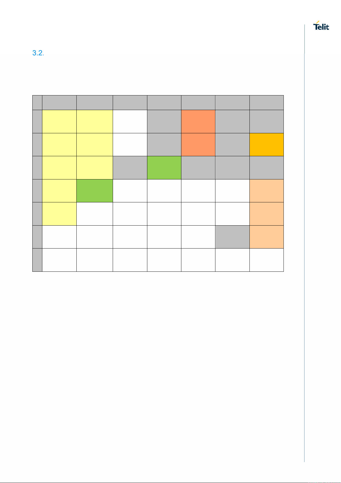
LGA Pads Layout
TOP VIEW
A B C D E F G
1
2 SPI_CLK SPI_MOSI
RTS CTS RES GND VBATT GND GND
RES GND VBATT GND ANT
3 SPI_MISO SPI_CS GND nHIB GND GND GND
4
5
6
7
TXD HOST_INTR RES RES RES RES RESET*
RXD RES RES RES RES RES ON_OFF
RES RES RES RES RES GND VDD
RES RES RES RES RES RES RES
1VV0301330 Rev. 3 Page 17 of 54 2018-03-13
Page 18

WE866 HW User Guide
4. POWER SUPPLY
Power Supply Requirements
The external power supply must be connected to VBATT signals and must fulfill the
following requirements:
Power Supply
Nominal Supply Voltage 3.8 V
Normal Operating Voltage Range 3.1 V÷ 4.50 V
The Operating Voltage Range MUST never be exceeded; care must
be taken when designing the application’s power supply section to
avoid having an excessive voltage drop.
If the voltage drop is exceeding the limits it could cause a Power Off of
the module.
Please note that the operating voltage limits MUST never be exceed,
including voltage overshoots and drops.
Power Consumption
The WE866 expected power consumption is reported on the table below. All values are at
25°C and VBATT=3.8V, if not otherwise stated.
1VV0301330 Rev. 3 Page 18 of 54 2018-03-13
Page 19

WE866 HW User Guide
Functional mode
Current consumption(*)
(typ)
[mA]
802.11b, 1Mbps 285
Transmission at
maximum power level
Reception
Idle connected 14
Peak calibration <400
Hibernate 0.03
(*) preliminary values
General Design Rules
802.11g, 6Mbps 261
802.11g, 54Mbps 236
802.11b, 1Mbps 66
802.11g, 54Mbps 66
The principal guidelines for the Power Supply Design embrace three different design steps:
The electrical design
The thermal design
Thermal PCB layout
4.3.1. Electrical Design Guidelines
The electrical design of the power supply depends strongly on the power source from which
this power is drained. We will distinguish them into three categories:
+5V input (typically PC internal regulator output)
+12V input (typically automotive)
Battery
1VV0301330 Rev. 3 Page 19 of 54 2018-03-13
Page 20

WE866 HW User Guide
4.3.1.1. +5V Source Power Supply Design Guidelines
Because of the small difference between the input and output voltage, a
switching converter is not the best choice, therefore a low-dropout regulator
is required.
When using a linear regulator, a proper heat sink must be provided in order
to dissipate the power generated.
A low-ESR, bypass capacitor of adequate capacity must be provided in
order to cut the current absorption peaks close to the WE866, a 100μF
tantalum capacitor is usually suited.
Make sure the low ESR capacitor on the power supply output (usually a
tantalum one) is rated at least 10V.
A protection diode should be inserted close to the power input, in order to
save the WE866 from power polarity inversion.
Guidelines
4.3.1.2. +12V Source Power Supply Design Guidelines
In this case, better efficiency of switching regulators can be exploited to
generate the required 3.8V
Switching frequencies of 500kHz or above are preferable, because of the
smaller inductor size and the faster transient response.
For car Pb battery, the input voltage can rise up to 15.8V and this should
be kept in mind when choosing components: all components in the power
supply must withstand this voltage. A spike protection diode has to be
inserted close to the power input.
A low-ESR, bypass capacitor of adequate capacity must be provided in
order to cut current absorption peaks. 100µF, 10V is usually enough.
A protection diode should be inserted close to the power input, to avoid
damage to the WE866 from polarity inversion. This can be the same diode
used for spike protection.
4.3.1.3. Battery Source Power Supply Design Guidelines
A single 3.7V Li-Ion cell battery can be used to power the WE866 module.
A low-ESR, bypass capacitor of adequate capacity must be provided in
order to cut current absorption peaks. 100µF, 10V is usually enough.
The WE866 module must be protected from polarity inversion: this can be
done with a protection diode, or by exploiting a suitable battery connector
1VV0301330 Rev. 3 Page 20 of 54 2018-03-13
Page 21

WE866 HW User Guide
Both three-cell Ni/Cd or Ni/MH 3.6V batteries, and 4V Pb batteries, can
feature maximum voltages above the maximum allowed VBATT for the
WE866, which is 4.5V. For this reason, they must not be directly
connected to the module. Only Li-Ion types are recommended for
direct connection.
4.3.2. Power Supply PCB layout Guidelines
As seen on the electrical design guidelines, the power supply shall have a lowESR capacitor on its output, to cut the current peaks, and a protection diode
on its input, to protect the VBATT pins from polarity inversion. The placement
of these components is crucial to ensure the correct working of the circuitry. A
misplaced component can be useless, or even detrimental to the power supply
performances.
The low-ESR, bypass capacitor must be placed close to the WE866
VBATT pads, or close to the inductor if a switching regulator is used.
The protection diode must be placed close to the input power connector.
The pcb power traces must be wide enough to ensure negligible voltage
drop even at the highest rated current consumption for the WE866.
Use of a good, common ground plane is recommended.
VDD Power Output
A regulated 1.85V supply voltage is provided on pin G6 of the WE866 module. Please note
that this voltage has the sole purpose to be a reference, e.g. for external voltage translators.
No external devices must be powered from this voltage.
1VV0301330 Rev. 3 Page 21 of 54 2018-03-13
Page 22

WE866 HW User Guide
5. DIGITAL SECTION
Logic Levels
The following table shows the logic level specifications use in WE866:
Parameter Min Max
Input level on any digital pin
(CMOS 1.8V) when on
-0.3V +2.1V
Level Min Max
VIH Input high level 1.5V 2.1V
VIL Input low level 0V 0.4V
VOH Output high level 1.6V 2.1V
VOL Output low level 0V 0.2V
VIL nRESET 0V 0.6V
The nRESET pin must be held below 0.6V for the device to register a reset.
Level Typical
Input current 5nA
Output current 6mA
Power On
The module is usually in state on mode. ON_OFF line is internally pulled up and when
VBATT is applied the module is automatically turned on.
The device need 3 ms to switch on the device and have all the internally voltage stable,
this soft start prevents excessive voltage drops of primary cells and rechargeable batteries
with high internal impedance. nRESET must be held low until the VBATT supply to the
device is driven and stable.
1VV0301330 Rev. 3 Page 22 of 54 2018-03-13
Page 23

WE866 HW User Guide
OFF
serve API calls
In order to switch on the device it must be applied a input logic high level to ON_OFF pin.
POWER
RESET
Device Ready to
ITEM NAME DESCRIPTION TYPICAL
T1 Supply settling time 3ms
T2 Hardware wake-up 25ms
T3 Initialization time Internal XTAL
stabilization plus
firmware initialization
time plus radio
calibration
1.35s
In order to switch off the device it’s necessary to force the ON_OFF pin to 0V.
1VV0301330 Rev. 3 Page 23 of 54 2018-03-13
Tip or Information – Don’t use any pull up resistor on the ON_OFF line,
it is internally pulled up.
Power Off
Page 24

WE866 HW User Guide
Low power deep sleep
The low power deep sleep (LPDS) mode is an energy-efficient and transparent sleep mode
that is entered automatically during periods of inactivity based on internal power
optimization algorithms. The device can wake up in less than 3ms from the internal timer or
from any incoming host command. Typical battery drain in this mode is 115µA. During LPDS
mode, the device retains the software state and certain configuration information. The
operation is transparent to the external host; thus, no additional handshake is required to
enter or exit this sleep mode.
Hibernate
The hibernate mode is the lowest power mode in which all of digital logic is power-gated.
Only a small section of the logic powered directly by the main input supply is retained. The
RTC is kept running and the device wakes up once the nHIB line is asserted by the host
device. Ultralow leakage when disabled (hibernate mode) with a current of less than 4 μA
with the RTC running. The average wake-up time is longer than LPDS mode, is about 50ms.
ITEM NAME DESCRIPTION MIN TYP MAX
THib
min
T
wakeup_Hib
(1) If temperature changes by more than 20°C, initialization time from HIB can increase
Minumum
hibernate time
Hardware wakeup
Minimum pulse width of nHIB
being low
(1) 50ms
time plus firmware
initialization time
by 200ms due to radio calibration.
10ms
Shutdown
The shutdown mode is the lowest power-mode system-wise. All device logics are off,
including the real.time clock (RTC). The wake-up time in this mode is longer than hibernate,
is about 1.1s.
1VV0301330 Rev. 3 Page 24 of 54 2018-03-13
Page 25

WE866 HW User Guide
State Wake-up Time Average Power
Consumption
Low Power Deep Sleep (LPDS) 3ms 115µA
Hibernate 50ms 4µA
Shutdown 1.1s 1µA
Communication ports
5.7.1. SPI
Module WE866 is considered as a slave when it is interfaced with a Host which acts as
master. In addition to the standard SPI lines (MOSI, MISO, CLK, CS) it can be used also
HOST_INT line. WE866 can interrupt the host using HOST_INT line to initiate the data
transfer over the interface. The SPI interface can work up to a speed of 20MHz.
PAD Signal I/O Function
B2 SPI_MOSI I Module data input, Host
data output
A3 SPI_MISO O Module data output, Host
data input
A2 SPI_CLK I SPI clock from Host to
module
B3 SPI_nCS I SPI Chip select (active low)
from Host
B4 HOST_INT O Interrupt from Module to
Host (Optional)
1VV0301330 Rev. 3 Page 25 of 54 2018-03-13
Page 26

WE866 HW User Guide
SPI_MISO
SPI_MISO
HOST_INT
5.7.2. UART
In the table below are listed the UART configuration of WE866.
PROPERTY WE866 CONFIGURATION
Baud rate 115200 bps, no auto-baud rate detection, can be changed by the
host up to 3 Mbps using a special command
Data bits 8 bits
Flow control CTS/RTS
Parity None
Stop bits 1
Bit order LSBit first
Host interrupt
Active high
polarity
Host interrupt
Rising edge or level 1
mode
Endianness Little-endian only, WE866 does not support automatic detection of
the host length while using the UART interface
1VV0301330 Rev. 3 Page 26 of 54 2018-03-13
Page 27

WE866 HW User Guide
PAD Signal I/O Function
A1 RTS I
Input for Request to send signal (RTS) from
DTE
B1 CTS O
A4 TXD I
A5 RXD O
Output for Clear to send signal (CTS) to DTE
Serial data input (TXD) from DTE
Serial data output (RXD) to DTE
B4 HOST_INT O Interrupt from Module to Host (Optional)
Figure.. shows the typical UART topology comprised of four standard UART lines (RTS,
CTS, TX and RX) plus an optional line INTERRUPT from WE866 module to the host
controller to allow efficient low-power mode. The configuration with INTERRUPT line offers
the maximum communication reliability and flexibility between the host and the module.
1VV0301330 Rev. 3 Page 27 of 54 2018-03-13
Page 28

WE866 HW User Guide
6. RF SECTION
Bands Variants
The WE866 module operates in the 2.400-2.500 GHz ISM band, and it complies with
protocols 802.11b/g/n. Supported channels are 1-13, at frequencies listed in the following
table:
Channel Frequency [MHz]
1 2412
2 2417
3 2422
4 2427
5 2432
6 2437
7 2442
8 2447
9 2452
10 2457
11 2462
12 2467
13 2472
1VV0301330 Rev. 3 Page 28 of 54 2018-03-13
Page 29

WE866 HW User Guide
Please note that channel availability may vary according to regional
regulations.
TX Output power
All measures have been taken at VBATT = 3.8V, Tamb = 25°C, if not otherwise stated.
Protocol
Datarate
[Mbps]
1 17
802.11b
802.11g
802.11n MCS7 12.0
2 17
11 17.25
6 16.25
9 16.25
54 13.5
Maximum RMS output
power (typ.) (*)
[dBm]
(*) preliminary values
Please note that maximum allowed output power may depend on
regional regulations.
1VV0301330 Rev. 3 Page 29 of 54 2018-03-13
Page 30

WE866 HW User Guide
RX Sensitivity
All measures have been taken at VBATT = 3.8V, Tamb = 25°C, if not otherwise stated.
Protocol
802.11b (PER < 8%)
802.11g (PER < 10%)
802.11n (PER < 10%)
Datarate
[Mbps]
Sensitivity (typ.)(*)
[dBm]
1 -94.7
2 -92.6
11 -87.0
6 -89.0
9 -88.0
54 -73.0
MCS0 -88.0
1
MCS7 -70.0
MCS7 (mixed mode) -69.0
(*) preliminary values
Antenna requirements
Special care must be taken during the design of the RF section on the application board.
RF performance degradation, and infringements of emission limits,
may arise if the following recommendations are not respected.
1VV0301330 Rev. 3 Page 30 of 54 2018-03-13
Page 31

WE866 HW User Guide
A 50Ω antenna is required. Telit’s WE866 interface features an SMA connector for an
external antenna, but other choices are possible, such as a chip or a printed one. In case
an integrated or printed antenna is used, it is recommended to place it on the edge of the
application board.
Since it may be necessary to tune the antenna impedance to 50Ω, it is recommended to
foresee a PI matching network between the WE866 and the antenna, at least during first
prototyping: if not required, a series 0Ω-resistor can be used, leaving the two shunt
components unpopulated.
In order to be able to reuse Telit’s FCC certification, the antenna on the application board
shall have a gain equal to the one recommended by Telit, or lower.
6.4.1. PCB Design guidelines
The WE866 module provides a 50Ω antenna pad, which has to be routed to the antenna
connector (or the integrated antenna) by means of a transmission line.
It is vital that the impedance of this line is controlled to 50Ω. The line should be as short
as possible, and keep a constant cross section, without abrupt curves. It shall be isolated
from any other noise source: in particular, trace shall not be crossed by other lines in
adjacent layers. Instead, a continuous ground plane is recommended under the antenna
trace, and a ground via curtain should connect it to the coplanar ground planes.
As an example of a possible implementation, the details of the antenna trace on the WE866
interface board are described in this section.
A Grounded Coplanar Waveguide (G-CPW) line has been chosen, since this kind of
transmission line ensures good impedance control and can be implemented in an outer
PCB layer as needed in this case. A SMA female connector has been used to feed the line.
The interface board is realized on a FR4, 4-layers PCB. Substrate material is characterized
by relative permittivity εr = 4.6 ± 0.4 @ 1 GHz, TanD= 0.019 ÷ 0.026 @ 1 GHz.
A characteristic impedance of nearly 50 Ω is achieved using trace width of 1.1 mm,
clearance from coplanar ground plane = 0.3 mm each side. The line uses reference ground
plane on layer 3, while copper is removed from layer 2 underneath the line. Height of trace
above ground plane is 1.335 mm. Calculated characteristic impedance is 51.6 Ω, estimated
line loss is less than 0.1 dB. The line geometry is shown below:
1VV0301330 Rev. 3 Page 31 of 54 2018-03-13
Page 32

WE866 HW User Guide
6.4.2. PCB Guidelines in case of FCC Certification
1VV0301330 Rev. 3 Page 32 of 54 2018-03-13
Page 33

WE866 HW User Guide
7. MECHANICAL DESIGN
Drawing
1VV0301330 Rev. 3 Page 33 of 54 2018-03-13
Page 34

WE866 HW User Guide
8. APPLICATION PCB DESIGN
Footprint
Recommended footprint for the application:
1VV0301330 Rev. 3 Page 34 of 54 2018-03-13
Page 35

WE866 HW User Guide
In order to easily rework the WE866 is suggested to consider on the application a 1.5 mm
placement inhibit area around the module.
1VV0301330 Rev. 3 Page 35 of 54 2018-03-13
Page 36

WE866 HW User Guide
It is also suggested, as common rule for an SMT component, to avoid having a
mechanical parts of the application in direct contact with the module.
Tip or Information – In the customer application, the region under
WIRING INHIBIT (see figure above) must be clear from signal or
ground paths.
PCB pad design
Non solder mask defined (NSMD) type is recommended for the solder pads on the PCB.
PCB pad dimensions
It is not recommended to place via or micro-via not covered by solder resist in an area of
0.3 mm around the pads unless it carries the same signal of the pad itself (see following
figure).
1VV0301330 Rev. 3 Page 36 of 54 2018-03-13
Page 37

WE866 HW User Guide
Holes in pad are allowed only for blind holes and not for through holes.
Recommendations for PCB pad surfaces:
Finish Layer thickness [µm] Properties
Electro-less Ni /
3 –7 / 0.03 – 0.15
Immersion Au
The PCB must be able to resist the higher temperatures which are occurring at the leadfree process. This issue should be discussed with the PCB-supplier. Generally, the
wettability of tin-lead solder paste on the described surface plating is better compared to
lead-free solder paste.
It is not necessary to panel the application PCB, however in that case it is suggested to
use milled contours and predrilled board breakouts; scoring or v-cut solutions are not
recommended.
Good solderability protection,
high shear force values
Stencil
Stencil’s apertures layout can be the same of the recommended footprint (1:1), we
suggest a thickness of stencil foil ≥ 120 µm.
1VV0301330 Rev. 3 Page 37 of 54 2018-03-13
Page 38

WE866 HW User Guide
Time maintained above:
Solder paste
Lead free
Solder paste
Sn/Ag/Cu
We recommend using only “no clean” solder paste in order to avoid the cleaning of the
modules after assembly.
Solder Reflow
Recommended solder reflow profile
Profile Feature
Pb-Free Assembly
Average ramp-up rate (TL to TP) 3°C/second max
Preheat
– Temperature Min (Tsmin)
– Temperature Max (Tsmax)
– Time (min to max) (ts)
Tsmax to TL
– Ramp-up Rate
1VV0301330 Rev. 3 Page 38 of 54 2018-03-13
150°C
200°C
60-180 seconds
3°C/second max
Page 39

WE866 HW User Guide
Ramp-down Rate
Time 25°C to Peak Temperature
– Temperature (TL)
– Time (tL)
217°C
60-150 seconds
Peak Temperature (Tp) 245 +0/-5°C
Time within 5°C of actual Peak
Temperature (tp)
10-30 seconds
6°C/second max.
8 minutes max.
Tip or Information – All temperatures refer to topside of the package,
measured on the package body surface.
Caution or Warning –WE866 module withstands one reflow process
only.
1VV0301330 Rev. 3 Page 39 of 54 2018-03-13
Page 40

WE866 HW User Guide
9. PACKAGING
Tray
The WE866 modules are packaged on trays of 98 pieces each when small quantities are
required (i.e. for test and evaluation purposes).
1VV0301330 Rev. 3 Page 40 of 54 2018-03-13
Page 41

WE866 HW User Guide
Reel
The WE866 modules are packaged on reels of 200 pieces each, see picture below.
1VV0301330 Rev. 3 Page 41 of 54 2018-03-13
Page 42

WE866 HW User Guide
Caution or Warning –These trays can withstand at the maximum
temperature of 65°C.
1VV0301330 Rev. 3 Page 42 of 54 2018-03-13
Page 43

WE866 HW User Guide
Moisture sensitivity
The moisture sensitivity level of the Product is “3” according with standard IPC/JEDEC JSTD-020, take care of all the relative requirements for using this kind of components.
Moreover, the customer has to take care of the following conditions:
a) The shelf life of the Product inside of the dry bag is 12 months from the bag seal date,
when stored in a non-condensing atmospheric environment of < 40°C and < 90% RH.
b) Environmental condition during the production: <= 30°C / 60% RH according to
IPC/JEDEC J-STD-033B.
c) The maximum time between the opening of the sealed bag and the reflow process must
be 168 hours if condition b) “IPC/JEDEC J-STD-033B paragraph 5.2” is respected.
d) Baking is required if conditions b) or c) are not respected
e) Baking is required if the humidity indicator inside the bag indicates 10% RH or more.
1VV0301330 Rev. 3 Page 43 of 54 2018-03-13
Page 44

WE866 HW User Guide
10. CONFORMITY ASSESSMENT ISSUES
FCC/IC Regulatory notices
Modification statement
Telit has not approved any changes or modifications to this device by the user. Any changes
or modifications could void the user’s authority to operate the equipment.
Telit n’approuve aucune modification apportée à l’appareil par l’utilisateur, quelle qu’en soit
la nature. Tout changement ou modification peuvent annuler le droit d’utilisation de
l’appareil par l’utilisateur.
Interference statement
This device complies with Part 15 of the FCC Rules and Industry Canada licence-exempt
RSS standard(s). Operation is subject to the following two conditions: (1) this device may
not cause interference, and (2) this device must accept any interference, including
interference that may cause undesired operation of the device.
Le présent appareil est conforme aux CNR d'Industrie Canada applicables aux appareils
radio exempts de licence. L'exploitation est autorisée aux deux conditions suivantes : (1)
l'appareil ne doit pas produire de brouillage, et (2) l'utilisateur de l'appareil doit accepter tout
brouillage radioélectrique subi, même si le brouillage est susceptible d'en compromettre le
fonctionnement.
Wireless notice
This equipment complies with FCC and IC radiation exposure limits set forth for an
uncontrolled environment. The antenna should be installed and operated with minimum
distance of 20 cm between the radiator and your body. Antenna gain must be below:
Type
Gain
WE866A1-P
Dipole ½-wave antenna
RP-SMA connector
2.2 dBi
nel Cet appareil est conforme aux limites d'exposition aux rayonnements de la IC pour un
environnement non contrôlé. L'antenne doit être installé de façon à garder une distance
minimale de 20 centimètres entre la source de rayonnements et votre corps. Gain de
l'antenne doit être ci-dessous:
1VV0301330 Rev. 3 Page 44 of 54 2018-03-13
Page 45

WE866 HW User Guide
L'émetteur ne doit pas être colocalisé ni fonctionner conjointement avec à autre antenne ou
autre émetteur.
Type
Gain
WE866A1-P
Dipole ½-wave antenna
RP-SMA connector
2.2 dBi
FCC Class B digital device notice
This equipment has been tested and found to comply with the limits for a Class B digital
device, pursuant to part 15 of the FCC Rules. These limits are designed to provide
reasonable protection against harmful interference in a residential installation. This
equipment generates, uses and can radiate radio frequency energy and, if not installed and
used in accordance with the instructions, may cause harmful interference to radio
communications. However, there is no guarantee that interference will not occur in a
particular installation. If this equipment does cause harmful interference to radio or
television reception, which can be determined by turning the equipment off and on, the user
is encouraged to try to correct the interference by one or more of the following measures:
- Reorient or relocate the receiving antenna. - Increase the separation between the
equipment and receiver. - Connect the equipment into an outlet on a circuit different from
that to which the receiver is connected. - Consult the dealer or an experienced radio/TV
technician for help.
Labelling Requirements for the Host device
The host device shall be properly labelled to identify the modules within the host device.
The certification label of the module shall be clearly visible at all times when installed in the
host device, otherwise the host device must be labelled to display the FCC ID and IC of the
module, preceded by the words "Contains transmitter module", or the word "Contains", or
similar wording expressing the same meaning, as follows:
Contains FCC ID: RI7WE866A1P Contains IC: 5131A- WE866A1P
L'appareil hôte doit être étiqueté comme il faut pour permettre l'identification des modules
qui s'y trouvent. L'étiquette de certification du module donné doit être posée sur l'appareil
hôte à un endroit bien en vue en tout temps. En l'absence d'étiquette, l'appareil hôte doit
porter une étiquette donnant le FCC ID et le IC du module, précédé des mots « Contient un
module d'émission », du mot « Contient » ou d'une formulation similaire exprimant le même
sens, comme suit :
Contains FCC ID: RI7WE866A1P Contains IC: 5131A- WE866A1P
1VV0301330 Rev. 3 Page 45 of 54 2018-03-13
Page 46

WE866 HW User Guide
CAN ICES-3 (B) / NMB-3 (B)
This Class B digital apparatus complies with Canadian ICES-003.
Cet appareil numérique de classe B est conforme à la norme canadienne ICES-003
1VV0301330 Rev. 3 Page 46 of 54 2018-03-13
Page 47

WE866 HW User Guide
2014/53/EU Directive
This device has been evaluated against the essential requirements of the
2014/53/EU Directive.
Bulgarian
Croatian
Czech
Danish
Dutch
English
Estonian
German
С настоящето “Telit Communications S.P.A.” декларира, че “WE866” отговаря на
съществените изисквания и другите приложими изисквания на Директива 2014/53/ЕС.
Ovime “Telit Communications S.P.A.”, izjavljuje da je ovaj “WE866 MODULE” je u skladu s
osnovnim zahtjevima i drugim relevantnim odredbama Direktive 2014/53/EU.
“Telit Communications S.P.A.” tímto prohlašuje, že tento “WE866 MODULE” je ve shodě se
základními požadavky a dalšími příslušnými ustanoveními směrnice 2014/53/ES.
Undertegnede “Telit Communications S.P.A.” erklærer herved, at følgende udstyr “WE866
MODULE” overholder de væsentlige krav og øvrige relevante krav i direktiv 2014/53/EF.
Hierbij verklaart “Telit Communications S.P.A.” dat het toestel “WE866 MODULE” in
overeenstemming is met de essentiële eisen en de andere relevante bepalingen van richtlijn
2014/53/EG.
Hereby, “Telit Communications S.P.A.”, declares that this “WE866 MODULE” is in compliance
with the essential requirements and other relevant provisions of Directive 2014/53/EU.
Käesolevaga kinnitab “Telit Communications S.P.A.” seadme “WE866 MODULE” vastavust
direktiivi 2014/53/EÜ põhinõuetele ja nimetatud direktiivist tulenevatele teistele asjakohastele
sätetele.
Hiermit erklärt “Telit Communications S.P.A.”, dass sich das Gerät “WE866 MODULE” in
Übereinstimmung mit den grundlegenden Anforderungen und den übrigen einschlägigen
Bestimmungen der Richtlinie 2014/53/EG befindet.
Greek
Hungarian
Finnish
French
Icelandic
Italian
Latvian
ΜΕ ΤΗΝ ΠΑΡΟΥΣΑ “Telit Communications S.P.A.” ΔΗΛΩΝΕΙ ΟΤΙ “WE866 MODULE”
ΣΥΜΜΟΡΦΩΝΕΤΑΙ ΠΡΟΣ ΤΙΣ ΟΥΣΙΩΔΕΙΣ ΑΠΑΙΤΗΣΕΙΣ ΚΑΙ ΤΙΣ ΛΟΙΠΕΣ ΣΧΕΤΙΚΕΣ
ΔΙΑΤΑΞΕΙΣ ΤΗΣ ΟΔΗΓΙΑΣ 2014/53/ΕΚ.
Alulírott, “Telit Communications S.P.A.” nyilatkozom, hogy a “WE866 MODULE” megfelel a
vonatkozó alapvetõ követelményeknek és az 2014/53/EU irányelv egyéb elõírásainak.
“Telit Communications S.P.A.” vakuuttaa täten että “WE866 MODULE” tyyppinen laite on
direktiivin 2014/53/EY oleellisten vaatimusten ja sitä koskevien direktiivin muiden ehtojen
mukainen.
Par la présente “Telit Communications S.P.A.” déclare que l'appareil “WE866 MODULE” est
conforme aux exigences essentielles et aux autres dispositions pertinentes de la directive
2014/53/CE.
Hér með lýsir “Telit Communications S.P.A.” yfir því að “WE866 MODULE” er í samræmi við
grunnkröfur og aðrar kröfur, sem gerðar eru í tilskipun 2014/53/EU
Con la presente “Telit Communications S.P.A.” dichiara che questo “WE866 MODULE” è
conforme ai requisiti essenziali ed alle altre disposizioni pertinenti stabilite dalla direttiva
2014/53/CE.
Ar šo “Telit Communications S.P.A.” deklarē, ka “WE866 module” atbilst Direktīvas 2014/53/EK
būtiskajām prasībām un citiem ar to saistītajiem noteikumiem.
1VV0301330 Rev. 3 Page 47 of 54 2018-03-13
Page 48

WE866 HW User Guide
EN 62311:2008
Lithuanian
Maltese
Norwegian
Polish
Portuguese
Slovak
Slovenian
Spanish
Šiuo “Telit Communications S.P.A.” deklaruoja, kad šis “WE866 module” atitinka esminius
reikalavimus ir kitas 2014/53/EB Direktyvos nuostatas.
Hawnhekk, “Telit Communications S.P.A.”, jiddikjara li dan “WE866 module” jikkonforma malħtiġijiet essenzjali u ma provvedimenti oħrajn relevanti li hemm fid-Dirrettiva 2014/53/EU.
“Telit Communications S.P.A.” erklærer herved at utstyret “WE866 module” er i samsvar med
de grunnleggende krav og øvrige relevante krav i direktiv 2014/53/EF.
Niniejszym “Telit Communications S.P.A.” oświadcza, że “WE866 module” jest zgodny z
zasadniczymi wymogami oraz pozostałymi stosownymi postanowieniami Dyrektywy
2014/53/EU
“Telit Communications S.P.A.” declara que este “WE866 module” está conforme com os
requisitos essenciais e outras disposições da Directiva 2014/53/CE.
“Telit Communications S.P.A.” týmto vyhlasuje, že “OM12030/X00”
požiadavky a všetky príslušné ustanovenia Smernice 2014/53/ES.
“Telit Communications S.P.A.” izjavlja, da je ta “WE866 module” v skladu z bistvenimi
zahtevami in ostalimi relevantnimi določili direktive 2014/53/ES.
Por medio de la presente “Telit Communications S.P.A.” declara que “WE866 module” cumple
con los requisitos esenciales y cualesquiera otras disposiciones aplicables o exigibles de la
Directiva 2014/53/CE.
(*)
spĺňa základné
Härmed intygar “Telit Communications S.P.A.” att denna “WE866 module” står I
Swedish
överensstämmelse med de väsentliga egenskapskrav och övriga relevanta bestämmelser som
framgår av direktiv 2014/53/EG.
In order to satisfy the essential requirements of R&TTE Directive (2014/53/EU),
the product is compliant with the following standards:
RF spectrum use (R&TTE art. 3.2) EN 300 328 v2.1.1
EMC (R&TTE art. 3.1b) EN 301 489-1 V2.1.0
EN 301 489-17 V3.1.0
Health & Safety (R&TTE art. 3.1a) EN 60950-1:2006 + A2:2013
The conformity assessment procedure referred to in Article 10 and detailed in
Annex IV of Directive 2014/53/EU has been followed with the involvement of the
following Notified Body:
AT4 wireless, S.A.
1VV0301330 Rev. 3 Page 48 of 54 2018-03-13
Parque Tecnologico de Andalucía
C/ Severo Ochoa 2
29590 Campanillas – Málaga
SPAIN
Notified Body No: 1909
Page 49

WE866 HW User Guide
Thus, the following marking is included in the product:
There is no restriction for the commercialization of this device in all the countries of
the European Union.
Final product integrating this module must be assessed against essential
requirements of the 2014/53/EU (RED) Directive. It should be noted that
assessment does not necessarily lead to testing. Telit Communications S.p.A.
recommends carrying out the following assessments:
RF spectrum use (RED art 3.2) It will depend on the antenna used on the final
product
EMC (RED art 3.1b) Testing
Health & Safety (RED art 3.1a) Testing
1VV0301330 Rev. 3 Page 49 of 54 2018-03-13
Page 50

WE866 HW User Guide
11. SAFETY RECOMMENDATIONS
READ CAREFULLY
Be sure the use of this product is allowed in the country and in the environment required.
The use of this product may be dangerous and has to be avoided in the following areas:
Where it can interfere with other electronic devices in environments such as
hospitals, airports, aircrafts, etc.
Where there is risk of explosion such as gasoline stations, oil refineries, etc. It is the
responsibility of the user to enforce the country regulation and the specific
environment regulation.
Do not disassemble the product; any mark of tampering will compromise the warranty
validity. We recommend following the instructions of the hardware user guides for correct
wiring of the product. The product has to be supplied with a stabilized voltage source and
the wiring has to be conformed to the security and fire prevention regulations. The product
has to be handled with care, avoiding any contact with the pins because electrostatic
discharges may damage the product itself. Same cautions have to be taken for the SIM,
checking carefully the instruction for its use. Do not insert or remove the SIM when the
product is in power saving mode.
The system integrator is responsible for the functioning of the final product; therefore, care
has to be taken to the external components of the module, as well as any project or
installation issue, because the risk of disturbing the GSM network or external devices or
having impact on the security. Should there be any doubt, please refer to the technical
documentation and the regulations in force. Every module has to be equipped with a proper
antenna with specific characteristics. The antenna has to be installed with care in order to
avoid any interference with other electronic devices and has to guarantee a minimum
distance from the body (20 cm). In case this requirement cannot be satisfied, the system
integrator has to assess the final product against the SAR regulation.
The European Community provides some Directives for the electronic equipment
introduced on the market. All of the relevant information is available on the European
Community website:
http://ec.europa.eu/enterprise/sectors/rtte/documents/
The text of the Directive 99/05 regarding telecommunication equipment is available,
while the applicable Directives (Low Voltage and EMC) are available at:
http://ec.europa.eu/enterprise/sectors/electrical/
1VV0301330 Rev. 3 Page 50 of 54 2018-03-13
Page 51

WE866 HW User Guide
12. ACRONYMS
TTSC
USB
HS
DTE
UMTS
WCDMA
HSDPA
HSUPA
UART
HSIC
Telit Technical Support Centre
Universal Serial Bus
High Speed
Data Terminal Equipment
Universal Mobile Telecommunication System
Wideband Code Division Multiple Access
High Speed Downlink Packet Access
High Speed Uplink Packet Access
Universal Asynchronous Receiver Transmitter
High Speed Inter Chip
SIM
SPI
ADC
DAC
I/O
GPIO
CMOS
MOSI
MISO
CLK
Subscriber Identification Module
Serial Peripheral Interface
Analog – Digital Converter
Digital – Analog Converter
Input Output
General Purpose Input Output
Complementary Metal – Oxide Semiconductor
Master Output – Slave Input
Master Input – Slave Output
Clock
MRDY
1VV0301330 Rev. 3 Page 51 of 54 2018-03-13
Master Ready
Page 52

WE866 HW User Guide
SRDY
CS
RTC
PCB
ESR
VSWR
VNA
Slave Ready
Chip Select
Real Time Clock
Printed Circuit Board
Equivalent Series Resistance
Voltage Standing Wave Radio
Vector Network Analyzer
1VV0301330 Rev. 3 Page 52 of 54 2018-03-13
Page 53

WE866 HW User Guide
13. DOCUMENT HISTORY
Revision Date Changes
0 2016-10-27 First issue
1 2016-12-06 Updated Pin Out Table
2 2017-11-22 Update Par. 9- Packaging
3 2018-03-13 Updated Par.10- Conformity assessment issues
1VV0301330 Rev. 3 Page 53 of 54 2018-03-13
Page 54

Mod. 0805 2016-08 Rev.5
 Loading...