

Page 1

WE866C3
HW Design Guide
1VV0301495 Rev. 15 – 2021-03-31
Page 2

WE866C3 Hardware Design Guide
SPECIFICATIONS ARE SUBJECT TO CHANGE WITHOUT NOTICE
NOTICE
While reasonable efforts have been made to assure the accuracy of this document, Telit
assumes no liability resulting from any inaccuracies or omissions in this document, or from
use of the information obtained herein. The information in this document has been carefully
checked and is believed to be reliable. However, no responsibility is assumed for
inaccuracies or omissions. Telit reserves the right to make changes to any products
described herein and reserves the right to revise this document and to make changes from
time to time in content hereof with no obligation to notify any person of revisions or changes.
Telit does not assume any liability arising out of the application or use of any product,
software, or circuit described herein; neither does it convey license under its patent rights
or the rights of others.
It is possible that this publication may contain references to, or information about Telit
products (machines and programs), programming, or services that are not announced in
your country. Such references or information must not be construed to mean that Telit
intends to announce such Telit products, programming, or services in your country.
COPYRIGHTS
This instruction manual and the Telit products described in this instruction manual may be,
include or describe copyrighted Telit material, such as computer programs stored in
semiconductor memories or other media. Laws in the Italy and other countries preserve for
Telit and its licensors certain exclusive rights for copyrighted material, including the
exclusive right to copy, reproduce in any form, distribute and make derivative works of the
copyrighted material. Accordingly, any copyrighted material of Telit and its licensors
contained herein or in the Telit products described in this instruction manual may not be
copied, reproduced, distributed, merged or modified in any manner without the express
written permission of Telit. Furthermore, the purchase of Telit products shall not be deemed
to grant either directly or by implication, estoppel, or otherwise, any license under the
copyrights, patents or patent applications of Telit, as arises by operation of law in the sale
of a product.
COMPUTER SOFTWARE COPYRIGHTS
The Telit and 3rd Party supplied Software (SW) products described in this instruction
manual may include copyrighted Telit and other 3rd Party supplied computer programs
stored in semiconductor memories or other media. Laws in the Italy and other countries
preserve for Telit and other 3rd Party supplied SW certain exclusive rights for copyrighted
computer programs, including the exclusive right to copy or reproduce in any form the
copyrighted computer program. Accordingly, any copyrighted Telit or other 3rd Party
supplied SW computer programs contained in the Telit products described in this instruction
manual may not be copied (reverse engineered) or reproduced in any manner without the
express written permission of Telit or the 3rd Party SW supplier. Furthermore, the purchase
of Telit products shall not be deemed to grant either directly or by implication, estoppel, or
otherwise, any license under the copyrights, patents or patent applications of Telit or other
3rd Party supplied SW, except for the normal non-exclusive, royalty free license to use that
arises by operation of law in the sale of a product.
1VV0301495 Rev. 15 Page 2 of 64 2021-01-20
Page 3

WE866C3 Hardware Design Guide
USAGE AND DISCLOSURE RESTRICTIONS
I. License Agreements
The software described in this document is the property of Telit and its licensors. It is
furnished by express license agreement only and may be used only in accordance with the
terms of such an agreement.
II. Copyrighted Materials
Software and documentation are copyrighted materials. Making unauthorized copies is
prohibited by law. No part of the software or documentation may be reproduced,
transmitted, transcribed, stored in a retrieval system, or translated into any language or
computer language, in any form or by any means, without prior written permission of Telit
III. High Risk Materials
Components, units, or third-party products used in the product described herein are NOT
fault-tolerant and are NOT designed, manufactured, or intended for use as on-line control
equipment in the following hazardous environments requiring fail-safe controls: the
operation of Nuclear Facilities, Aircraft Navigation or Aircraft Communication Systems, Air
Traffic Control, Life Support, or Weapons Systems (High Risk Activities"). Telit and its
supplier(s) specifically disclaim any expressed or implied warranty of fitness for such HighRisk Activities.
IV. Trademarks
TELIT and the Stylized T Logo are registered in Trademark Office. All other product or
service names are the property of their respective owners.
V. Third Party Rights
The software may include Third Party Right software. In this case you agree to comply with
all terms and conditions imposed on you in respect of such separate software. In addition
to Third Party Terms, the disclaimer of warranty and limitation of liability provisions in this
License shall apply to the Third-Party Right software.
TELIT HEREBY DISCLAIMS ANY AND ALL WARRANTIES EXPRESS OR IMPLIED
FROM ANY THIRD PARTIES REGARDING ANY SEPARATE FILES, ANY THIRD PARTY
MATERIALS INCLUDED IN THE SOFTWARE, ANY THIRD PARTY MATERIALS FROM
WHICH THE SOFTWARE IS DERIVED (COLLECTIVELY “OTHER CODE”), AND THE
USE OF ANY OR ALL THE OTHER CODE IN CONNECTION WITH THE SOFTWARE,
INCLUDING (WITHOUT LIMITATION) ANY WARRANTIES OF SATISFACTORY
QUALITY OR FITNESS FOR A PARTICULAR PURPOSE.
NO THIRD PARTY LICENSORS OF OTHER CODE SHALL HAVE ANY LIABILITY FOR
ANY DIRECT, INDIRECT, INCIDENTAL, SPECIAL, EXEMPLARY, OR CONSEQUENTIAL
DAMAGES (INCLUDING WITHOUT LIMITATION LOST PROFITS), HOWEVER CAUSED
AND WHETHER MADE UNDER CONTRACT, TORT OR OTHER LEGAL THEORY,
ARISING IN ANY WAY OUT OF THE USE OR DISTRIBUTION OF THE OTHER CODE
OR THE EXERCISE OF ANY RIGHTS GRANTED UNDER EITHER OR BOTH THIS
LICENSE AND THE LEGAL TERMS APPLICABLE TO ANY SEPARATE FILES, EVEN IF
ADVISED OF THE POSSIBILITY OF SUCH DAMAGES.
1VV0301495 Rev. 15 Page 3 of 64 2021-01-20
Page 4

WE866C3 Hardware Design Guide
WE866C3-P
APPLICABILITY TABLE
PRODUCTS
1VV0301495 Rev. 15 Page 4 of 64 2021-01-20
Page 5
WE866C3 Hardware Design Guide
CONTENTS
NOTICE……………. ........................................................................................... 2
COPYRIGHTS .................................................................................................... 2
COMPUTER SOFTWARE COPYRIGHTS ........................................................ 2
USAGE AND DISCLOSURE RESTRICTIONS ................................................. 3
APPLICABILITY TABLE .................................................................................... 4
CONTENTS ........................................................................................................ 5
1. INTRODUCTION .............................................................................. 9
Scope ............................................................................................... 9
Audience........................................................................................... 9
Contact Information, Support ........................................................... 9
Text Conventions ........................................................................... 10
Related Documents ........................................................................ 11
2. GENERAL PRODUCT DESCRIPTION ......................................... 12
Overview......................................................................................... 12
Block Diagram ................................................................................ 12
Product Variants ............................................................................. 12
Target Market ................................................................................. 13
Main Features ................................................................................ 13
3. PINS ALLOCATION ...................................................................... 15
Pin Type Definition ......................................................................... 15
Pin-out ............................................................................................ 15
LGA Pads Layout ........................................................................... 17
4. POWER SUPPLY .......................................................................... 18
Power Supply Requirements ......................................................... 18
Power Consumption ....................................................................... 19
4.2.1. Typical Power Consumption for WLAN Low-Power States .......... 19
4.2.2. Typical Power Consumption for WLAN Continuous Rx [2.4 GHz] 19
4.2.3. Typical Power Consumption for WLAN Continuous Rx [5 GHz] ... 20
4.2.4. Typical Power Consumption for WLAN Continuous Tx [2.4 GHz] 20
4.2.5. Typical Power Consumption for WLAN Continuous Tx [5 GHz] ... 21
4.2.6. Typical Power consumption for BT ................................................ 21
Power Supply Sequencing ............................................................. 23
5. DIGITAL SPECIFICATION ............................................................ 24
DC Electrical Characteristics ......................................................... 24
Interface Ports and Signals ............................................................ 25
1VV0301495 Rev. 15 Page 5 of 64 2021-01-20
Page 6

WE866C3 Hardware Design Guide
5.2.1. WLAN Interfaces ............................................................................ 25
5.2.1.1. SDIO Interface................................................................................ 25
5.2.1.2. WL_EN ........................................................................................... 25
5.2.1.3. WOW .............................................................................................. 25
5.2.1.4. LF_CLK_IN ..................................................................................... 26
5.2.1.5. Coexistence Use Cases ................................................................. 26
BT Interface .................................................................................... 28
5.3.1.1. BT HCI-UART ................................................................................. 28
5.3.1.2. PCM/I2S ......................................................................................... 28
5.3.1.3. BT_EN ............................................................................................ 29
LE910Cx-WE866C3 Bundling Pin Map ......................................... 29
6. RF SPECIFICATION ...................................................................... 30
RF Frequencies .............................................................................. 30
Tx Output Power ............................................................................ 30
6.2.1. Tx Output Power at Room Temperature ....................................... 30
6.2.1.1. 802.11b (2.4GHz) ........................................................................... 30
6.2.1.2. 802.11g (2.4GHz) ........................................................................... 30
6.2.1.3. 802.11n, Channel BW = 20MHz (2.4GHz) .................................... 31
6.2.1.4. 802.11n, Channel BW = 40MHz (2.4GHz) .................................... 31
6.2.1.5. 802.11a (5GHz) .............................................................................. 31
6.2.1.6. 802.11n/ac, Channel BW = 20MHz (5GHz) .................................. 31
6.2.1.7. 802.11n/ac, Channel BW = 40MHz (5GHz) .................................. 32
6.2.1.8. 802.11ac, Channel BW = 80MHz (5GHz) ..................................... 32
6.2.1.9. Bluetooth TX Power ....................................................................... 32
6.2.2. Tx Output Power at Cold Temperature .......................................... 32
6.2.2.1. 802.11b (2.4GHz) ........................................................................... 32
6.2.2.2. 802.11g (2.4GHz) ........................................................................... 32
6.2.2.3. 802.11n, Channel BW = 20MHz (2.4GHz) .................................... 33
6.2.2.4. 802.11n, Channel BW = 40MHz (2.4GHz) .................................... 33
6.2.2.5. 802.11a (5GHz) .............................................................................. 33
6.2.2.6. 802.11n/ac, Channel BW = 20MHz (5GHz) .................................. 33
6.2.2.7. 802.11n/ac, Channel BW = 40MHz (5GHz) .................................. 34
6.2.2.8. 802.11ac, Channel BW = 80MHz (5GHz) ..................................... 34
6.2.3. Tx Output Power at Hot Temperature ........................................... 34
6.2.3.1. 802.11b (2.4GHz) ........................................................................... 34
6.2.3.2. 802.11g (2.4GHz) ........................................................................... 34
6.2.3.3. 802.11n, Channel BW = 20MHz (2.4GHz) .................................... 34
6.2.3.4. 802.11n, Channel BW = 40MHz (2.4GHz) .................................... 35
1VV0301495 Rev. 15 Page 6 of 64 2021-01-20
Page 7

WE866C3 Hardware Design Guide
6.2.3.5. 802.11a (5GHz) .............................................................................. 35
6.2.3.6. 802.11n/ac, Channel BW = 20MHz (5GHz) .................................. 35
6.2.3.7. 802.11n/ac, Channel BW = 40MHz (5GHz) .................................. 35
6.2.3.8. 802.11ac, Channel BW = 80MHz (5GHz) ..................................... 35
Receiver Sensitivity ........................................................................ 36
6.3.1. Receiver Sensitivity at Room Temperature ................................... 36
6.3.1.1. 802.11b (2.4GHz) ........................................................................... 36
6.3.1.2. 802.11g (2.4GHz) ........................................................................... 36
6.3.1.3. 802.11n, Channel BW = 20MHz (2.4GHz) .................................... 36
6.3.1.4. 802.11n, Channel BW = 40MHz (2.4GHz) .................................... 37
6.3.1.5. 802.11a (5GHz) .............................................................................. 37
6.3.1.6. 802.11n/ac, Channel BW = 20MHz (5GHz) .................................. 37
6.3.1.7. 802.11n/ac, Channel BW = 40MHz (5GHz) .................................. 37
6.3.1.8. 802.11ac, Channel BW = 80MHz (5GHz) ..................................... 38
6.3.1.9. Bluetooth (BER < 0.1%) ................................................................. 38
6.3.2. Receiver Sensitivity at Cold Temperature ..................................... 38
6.3.2.1. 802.11b (2.4GHz) ........................................................................... 38
6.3.2.2. 802.11g (2.4GHz) ........................................................................... 38
6.3.2.3. 802.11n, Channel BW = 20MHz (2.4GHz) .................................... 39
6.3.2.4. 802.11n, Channel BW = 40MHz (2.4GHz) .................................... 39
6.3.2.5. 802.11a (5GHz) .............................................................................. 39
6.3.2.6. 802.11n/ac, Channel BW = 20MHz (5GHz) .................................. 39
6.3.2.7. 802.11n/ac, Channel BW = 40MHz (5GHz) .................................. 40
6.3.2.8. 802.11ac, Channel BW = 80MHz (5GHz) ..................................... 40
6.3.3. Receiver Sensitivity at Hot Temperature ....................................... 40
6.3.3.1. 802.11b (2.4GHz) ........................................................................... 40
6.3.3.2. 802.11g (2.4GHz) ........................................................................... 40
6.3.3.3. 802.11n, Channel BW = 20MHz (2.4GHz) .................................... 40
6.3.3.4. 802.11n, Channel BW = 40MHz (2.4GHz) .................................... 41
6.3.3.5. 802.11a (5GHz) .............................................................................. 41
6.3.3.6. 802.11n/ac, Channel BW = 20MHz (5GHz) .................................. 41
6.3.3.7. 802.11n/ac, Channel BW = 40MHz (5GHz) .................................. 41
6.3.3.8. 802.11ac, Channel BW = 80MHz (5GHz) ..................................... 41
7. DESIGN GUIDELINES .................................................................. 42
General PCB Design Guidelines ................................................... 42
SDIO Interface................................................................................ 42
Voltage Regulator .......................................................................... 42
7.3.1. Recommended Regulators ............................................................ 42
1VV0301495 Rev. 15 Page 7 of 64 2021-01-20
Page 8
WE866C3 Hardware Design Guide
7.3.2. Regulator Operating Conditions .................................................... 43
7.3.3. ESD and Thermal Information ....................................................... 44
Antenna Requirements .................................................................. 45
7.4.1. Main Antenna ................................................................................. 45
7.4.2. Antenna Cable................................................................................ 45
7.4.3. Antenna Design .............................................................................. 46
7.4.4. Antenna Installation Guidelines ..................................................... 47
8. MECHANICAL DESIGN ................................................................ 48
Mechanical Dimensions ................................................................. 48
8.1.1. Mechanical Drawing ....................................................................... 48
8.1.1.1. Top View......................................................................................... 48
8.1.1.2. Bottom View ................................................................................... 49
8.1.1.3. Side View ....................................................................................... 50
9. APPLICATION PCB DESIGN ....................................................... 51
Recommended Footprint for the Application ................................. 51
PCB Pad Design ............................................................................ 52
PCB Pad Dimensions..................................................................... 53
Stencil ............................................................................................. 54
Solder Paste ................................................................................... 54
Cleaning ......................................................................................... 54
Solder Reflow ................................................................................. 55
10. PACKING SYSTEM ....................................................................... 56
Tray ................................................................................................ 56
Tray Drawing .................................................................................. 57
Moisture Sensitivity ........................................................................ 58
11. CONFORMITY ASSESSMENT ISSUES ...................................... 59
Declaration of Conformity .............................................................. 59
Product Regulatory Compliance Markings .................................... 59
12. SAFETY RECOMMENDATIONS .................................................. 60
READ CAREFULLY ....................................................................... 60
13. ACRONYMS .................................................................................. 61
14. DOCUMENT HISTORY ................................................................. 62
1VV0301495 Rev. 15 Page 8 of 64 2021-01-20
Page 9

WE866C3 Hardware Design Guide
1. INTRODUCTION
Scope
This document introduces the Telit WE866C3 module and presents possible and
recommended hardware solutions for developing a product based on this module.
Obviously, this document cannot include every hardware solution or every product that can
be designed. Where the suggested hardware configurations need not be considered
mandatory, the information given should be used as a guide and a starting point for properly
developing your product with the Telit module.
Audience
This document is intended for Telit customers, especially system integrators, about to
implement their applications using the Telit module.
Contact Information, Support
For general contact, technical support services, technical questions and report
documentation errors contact Telit Technical Support at:
• TS-EMEA@telit.com
• TS-AMERICAS@telit.com
• TS-APAC@telit.com
• TS-SRD@telit.com
Alternatively, use:
https://www.telit.com/contact-us/
For detailed information about where you can buy the Telit modules or for recommendations
on accessories and components visit:
https://www.telit.com
Our aim is to make this guide as helpful as possible. Keep us informed of your comments
and suggestions for improvements.
Telit appreciates feedback from the users of our information.
1VV0301495 Rev. 15 Page 9 of 64 2021-01-20
Page 10
WE866C3 Hardware Design Guide
This information MUST be followed or catastrophic
Alerts the user to important points about
Provides advice and suggestions that may be
Text Conventions
Danger –
equipment failure or bodily injury may occur.
Caution or Warning –
integrating the module, if these points are not followed, the module and
end user equipment may fail or malfunction.
Tip or Information –
useful when integrating the module.
All dates are in ISO 8601 format, i.e. YYYY-MM-DD.
1VV0301495 Rev. 15 Page 10 of 64 2021-01-20
Page 11

WE866C3 Hardware Design Guide
Related Documents
• LE910Cx HW Design Guide 1VV0301298
• Telit EVB User Guide 1VV0301249
• LE910Cx Multi Technology Interface 1VV0301508
Board TLB - HW User Guide
1VV0301495 Rev. 15 Page 11 of 64 2021-01-20
Page 12
WE866C3 Hardware Design Guide
QCA9377
5G
Fil ter
5G
PA
Diplexer
2.4G
Fil ter
48MH z
XO
TX/RX
TX/RX
SDI O
WL_EN
WO W
LT E_COEX
32K_IN
3.3V
VDD_IO
BT_UART
BT_EN
I2S/PCM
Cou pler
ANT
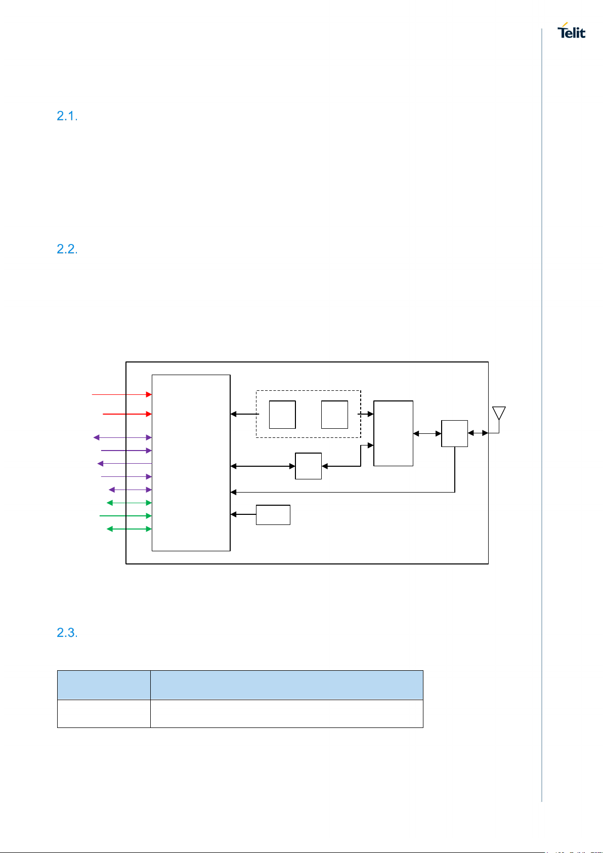
2. GENERAL PRODUCT DESCRIPTION
Overview
The WE866C3 is a low power and low-cost WIFI/BT wireless module solution based on
Qualcomm QCA9377-3. It supports 1×1 IEEE 802.11a/b/g/n/ac WLAN standards and BT
4.2 + HS + BLE, enabling seamless integration of WLAN/BT and low energy. It is a perfect
companion solution for Telit cellular modules such as LE910Cx or LE920A4.
WE866C3 supports low-power SDIO 3.0 interface for WLAN and a UART/PCM interface
for BT. WE866C3 also supports BT-WLAN coexistence and uses the 2-wire ISM-LTE
coexistence interface.
Block Diagram
The following figure shows a high-level block diagram of WE866C3 module and its major
functional blocks.
• Power supply
• SDIO
• PCM and UART
• RF Antenna
Figure 1 WE866C3 Module Block Diagram
Product Variants
WE866C3 variants are listed below:
Product Description
WE866C3-P 1x1 WIFI/BT wireless module
1VV0301495 Rev. 15 Page 12 of 64 2021-01-20
Page 13
WE866C3 Hardware Design Guide
Target Market
WE866C3 can be used in IoT applications complementing client data availability coverage
of the Cellular modems, with low power and low cost, for example:
• Bridging LTE / WLAN
• Industrial floor
• Healthcare instrument data terminals
• Smart Home automation and remote control
Main Features
Feature Specification
Power
Interfaces
Supported
Data Rate
Main supply voltage: 3.3V
VIO supply voltage: 1.8V or 3.3V
WLAN SDIO 3.0
BT UART
BT PCM/I2S
LTE Coexistence UART (WCI)
Low frequency 32.768KHz sleep clock
Single Antenna port, 50 Ohm
Control signals
802.11a (5GHz): 6, 9, 12, 18, 24, 36, 48, 54Mbps
802.11b (2.4GHz): 1, 2, 5.5, 11Mbps
802.11g (2.4GHz): 6, 9, 12, 18, 24, 36, 48, 54Mbps
802.11n (2.4GHz/5GHz):
• 20Mhz BW: Up to 72.2Mbps using short GI (MCS0-7)
• 40Mhz BW: Up to 144.4Mbps using short GI (MCS0-7)
802.11ac (5GHz): HT20 (MCS0-8), VHT40 (MCS0-9), VHT80 (MCS0-9)
802.11a / 54Mbps: 14 dbm
802.11b / 11Mbps: 18 dbm
802.11g / 54Mbps: 15 dbm
Transmission
Power
802.11n / HT20 (MCS7): 15 dbm
802.11ac / HT20 (MCS0): 15.5 dbm
802.11ac / VHT40 (MCS9): 11 dbm
802.11ac / VHT80 (MCS9): 10.5 dbm
1VV0301495 Rev. 15 Page 13 of 64 2021-01-20
Page 14
WE866C3 Hardware Design Guide
Data
Standard
Operating
Modes
IEEE 802.11a/b/g/n/ac
Access Point
Station
Modulation BPSK, QPSK, CCK, 16QAM, 64QAM, 256QAM
Size: 15±0.15 x 13±0.15 x 2.15±0.15 mm
Mechanical
Package: LGA
Weight: 1g
1)
Temperature
Range
Operating: -30°C to +85°C
Storage and non-operating: -40°C to +105°C
RoHS All hardware components are fully compliant with EU RoHS directive
Notes:
1) The module complies with IEEE standard.
1VV0301495 Rev. 15 Page 14 of 64 2021-01-20
Page 15
WE866C3 Hardware Design Guide
BT UART interface
B3
BT_CTS
VIO
DI
Bluetooth HCI-UART CTS signal
B4
BT_RTS
VIO
DO
Bluetooth HCI-UART RTS signal
A5
BT_RXD
VIO
DI
Bluetooth HCI-UART RXD signal
A4
BT_TXD
VIO
DO
Bluetooth HCI-UART TXD signal
BT PCM interface
C6
BT_I2S_SDI
VIO
DI, PU
Bluetooth PCM/I2S Input signal, Internal Pull-Up
C5
BT_I2S_WS
VIO B Bluetooth PCM/I2S Frame Sync signal
D5
BT_I2S_SCK
VIO
B, PD
Bluetooth PCM/I2S Bit CLK signal
D6
BT_I2S_SDO
VIO
DO
Bluetooth PCM/I2S output signal
Low power Clock signal
B5
LF_CLK_IN
VIO
DI, PD
External low–power 32.768 kHz clock input
Host wake pins
OD,
PU
Wake on Wireless. WIFI/BT Wakeup host.
Active Low, Internal Pull-Up
SDIO 3.0 interface
D7
SDIO_CLK
VIO
DI, PU
SDIO clock signal Input, Internal Pull-Up
E7
SDIO_CMD
VIO B SDIO CMD line signal
C7
SDIO_D0
VIO B SDIO data bus D0
B6
SDIO_D1
VIO B SDIO data bus D1
A6
SDIO_D2
VIO
B, PU
SDIO data bus D2, Internal Pull-Up
B7
SDIO_D3
VIO B SDIO data bus D3
signals
/ AUX UART RXD
Secondary UART - LTE coexistence UART_TXD
/ AUX_UART_TXD
3. PINS ALLOCATION
Pin Type Definition
Type Description
DI Digital Input
DO Digital Output
PD Pull-Down
PU Pull-Up
OD Open-Drain Output
B Bi-Directional
AI Analog/RF Input
AO Analog/RF Output
P Power Input
Note: Pins directions are with respect to the WE866C3 module.
Pin-out
Pin Pin Name
D4 WOW VIO
Pin Reference
Voltage
Pin
Type
Pin Description
Coexistence and control
C3 LTE_UART_RX VIO DI, PU
C4 LTE_UART_TX VIO DO
1VV0301495 Rev. 15 Page 15 of 64 2021-01-20
Secondary UART - LTE coexistence UART RXD
Page 16
WE866C3 Hardware Design Guide
G5
WL_EN
VIO
DI, PD
WLAN enable (Active high)
G6
BT_EN
VIO
DI, PD
Bluetooth enable (Active high)
RF Antennas
Antenna 1 - Main Antenna for modules with a
single antenna configuration
G3
RFU ANT2
NA
NA
Reserved for Antenna 2.
Power
A1
VDD_3.3V
3.13 V to 3.46 V
P
Main Input voltage (WIFI & BT)
A2
VDD_3.3V
3.13 V to 3.46 V
P
Main Input voltage (WIFI & BT)
A3
VDDIO
1.8 V or 3.3 V
P
Voltage supply for all I/O signals (1.71V - 3.46V)
A7
GND
– – Power Ground
B1
GND
– – Power Ground
B2
GND
– – Power Ground
C1
GND
– – Power Ground
C2
GND
– – Power Ground
D2
GND
– – Power Ground
E1
GND
– – Power Ground
E2
GND
– – Power Ground
F1
GND
– – Power Ground
F2
GND
– – Power Ground
F3
GND
– – Power Ground
F4
GND
– – Power Ground
G2
GND
– – Power Ground
G4
GND
– – Power Ground
G7
GND
– – Power Ground
Factory use
D3
RFU
NC - Reserved for future use. No connect.
E3
RFU
NC - Reserved for future use. No connect.
E4
RFU
NC - Reserved for future use. No connect.
E5
RFU
NC - Reserved for future use. No connect.
E6
RFU
NC - Reserved for future use. No connect.
F5
RFU
NC - Reserved for future use. No connect.
F6
RFU
NC - Reserved for future use. No connect.
F7
RFU
NC - Reserved for future use. No connect.
G1
RFU
NC - Reserved for future use. No connect.
Pin Pin Name
D1 ANT1 A AI, AO
Pin Reference
Voltage
Pin
Type
Pin Description
1VV0301495 Rev. 15 Page 16 of 64 2021-01-20
Page 17
WE866C3 Hardware Design Guide
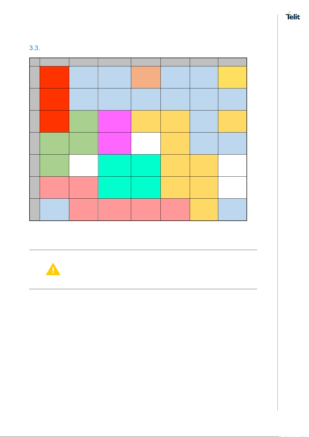
LGA Pads Layout
A B C D E F G
1 VDD_3.3V GND GND ANT1 GND GND RFU
2 VDD_3.3V GND GND GND GND GND GND
3 VDDIO
BT_TXD
4
5
6 SDIO_D2 SDIO_D1
7 GND SDIO_D3 SDIO_D0
(O)
BT_RXD
(I)
BT_CTS
(I)
BT_RTS
(O)
LF_CLK_IN
(I)
LTE_UART_RX
(I)
LTE_UART_TX
(O)
BT_I2S_WS
(I)
BT_I2S_SDI
(I)
RFU RFU GND RFU (ANT2)
WOW
(OD)
BT_I2S_SCK
(I)
BT_I2S_SDO
(O)
SDIO_CLK
(I)
RFU GND GND
RFU RFU
RFU RFU
SDIO_CMD RFU GND
WL_EN
(I)
BT_EN
(I)
TOP VIEW
WARNING
Reserved pins must not be connected.
1VV0301495 Rev. 15 Page 17 of 64 2021-01-20
Page 18
WE866C3 Hardware Design Guide
4. POWER SUPPLY
The power supply circuitry and board layout are a very important part in the full product
design and they strongly reflect on the product overall performances, hence read carefully
the requirements and the guidelines that will follow for a proper design.
Power Supply Requirements
There are two power supply inputs to the module. The main power supply, connected to
VDD_3.3V input and the VDDIO input, each must fulfill the following requirements:
VDD_3.3V Input Minimum Maximum
Absolute Maximum Voltage -0.3 V 3.65 V
Nominal Supply Voltage 3.3 V -
Normal Operating Voltage Range 3.135 V 3.465 V
VDDIO Input Minimum Maximum
Absolute Maximum Voltage -0.3 V 4.0 V
Nominal Supply Voltage 1.8V or 3.3V -
Normal Operating Voltage Range 1.71 V 3.46 V
NOTE:
The Maximum Voltage MUST never be exceeded; care must be
taken when designing the application’s power supply section to avoid
having an excessive voltage drop.
If the voltage drop is exceeding the limits it could lead to degradation
of performance or cause a Power Off of the module.
1VV0301495 Rev. 15 Page 18 of 64 2021-01-20
Page 19
WE866C3 Hardware Design Guide
Total power
(VDDIO = 1.8V)
Total power consumption [mA]
(VDDIO = 1.8V)
Power Consumption
The below tables provides the typical current consumption values of the module for the
various available modes.
4.2.1. Typical Power Consumption for WLAN Low-Power States
Mode
Standby 0.2 Deep Sleep
Power Save, 2.4GHz
Power Save, 5GHz
4.2.2. Typical Power Consumption for WLAN Continuous Rx [2.4 GHz]
consumption [mA]
1.3 DTIM=1
0.8
0.6 DTIM=10
1.5 DTIM=1
0.9 DTIM=3
0.7 DTIM=10
Mode Description
DTIM=3
Rate
11b 1Mbps 60
11b 11Mbps 62
11g 54Mbps
MCS0 HT20
MCS7 HT20
70
67
69
1VV0301495 Rev. 15 Page 19 of 64 2021-01-20
Page 20
WE866C3 Hardware Design Guide
Total Power Consumption [mA]
(VDDIO = 1.8V)
Total Power Consumption [mA]
(VDDIO = 1.8V)
4.2.3. Typical Power Consumption for WLAN Continuous Rx [5 GHz]
Rate
MCS0 HT20 96
MCS7 HT20 94
MCS8 VHT20
MCS0 HT40 94
MCS7 HT40 99
MCS8 VHT40 115
MCS9 VHT40 100
MCS7 VHT80 130
MCS8 VHT80 162
MCS9 VHT80 131
4.2.4. Typical Power Consumption for WLAN Continuous Tx [2.4 GHz]
112
Rate
11b 1Mbps 365
11b 11Mbps 362
11g 54Mbps 340
MCS0 HT20 348
MCS7 HT20 335
1VV0301495 Rev. 15 Page 20 of 64 2021-01-20
Page 21

WE866C3 Hardware Design Guide
Total Power Consumption [mA]
(VDDIO = 1.8V)
Total Power Consumption [mA]
(VDDIO = 1.8V)
4.2.5. Typical Power Consumption for WLAN Continuous Tx [5 GHz]
Rate
MCS0 HT20 495
MCS7 HT20 432
MCS8 VHT20 422
MCS0 HT40
MCS7 HT40 435
MCS8 VHT40 432
MCS9 VHT40 429
MCS7 VHT80 440
MCS8 VHT80 438
MCS9 VHT80
4.2.6. Typical Power consumption for BT
Rate
Continuous Rx burst 25
Continuous TX Class 2 (+4 dBm) 42
475
436
Continuous TX Class 2 (+12.5 dBm) 70
1.28 sec page scan (non-interlaced)
1.28 sec LE ADV 0.23
1.28 sec Sniff as master 0.21
1.28 sec Sniff as slave 0.26
1VV0301495 Rev. 15 Page 21 of 64 2021-01-20
0.36
Page 22

WE866C3 Hardware Design Guide
NOTE:
Current consumptions specification refers to typical samples and
typical material.
Values represent an average measurement done over few seconds.
Values may vary depending on network and environmental
conditions.
Power consumptions values obtained with VDD_3.3V = 3.3V and
VDDIO = 1.8V.
NOTE:
Current consumption is measured at the system level and is the sum
of both VDD_3.3V and VDDIO current consumpotions.
NOTE:
Current consumption related to WLAN and BT TX cases are
measured at typical TX output power as listed in 6.2.
1VV0301495 Rev. 15 Page 22 of 64 2021-01-20
Page 23

WE866C3 Hardware Design Guide
VBATT
VDD IO
VDD_3.3V
WL_EN
BT_EN
LF_CLK_IN
Powe r up N ormal Ope ration Powe r downNorm al OperationReset
90% of VDDIO to 10% of 3.3V
Minimum 0 Sec
90% of 3.3V to WL_E N and BT_EN high
Minimum 10 uSec
WLAN_EN valid to LF_CLK_IN
Minim um 0 Sec
WL_EN and BT_EN low to 90% of 3.3V
Minim um 10 uSec
might damage the device and
Power Supply Sequencing
The recommended power sequence between VDD_3.3V and VDDIO inputs is as shown
below:
Notes:
1. VDDIO voltage should match VIO voltage of the host. In some applications, it may
connect to 3.3 V matching the Host VIO voltage.
2. All host interface signals must stay floating or low before valid power on sequence
WL_EN/BT_EN = ”High”, and after WL_EN/BT_EN = “Low”.
Warning:
Please carefully follow the recommended power Up/Down sequencing.
Not following the recommended procedure
consequently void the warranty.
1VV0301495 Rev. 15 Page 23 of 64 2021-01-20
Page 24

WE866C3 Hardware Design Guide
5. DIGITAL SPECIFICATION
DC Electrical Characteristics
Parameter Min Typical Max Unit
High-level input voltage 0.7 * VDDIO - VDDIO + 0.3 V
Low-level input voltage -0.3 - 0.3 * VDDIO V
Input low leakage current
(VIN = 0 V Supply =
VDDIO max)
-5.0 0 5.0 μA
Input pull resistor
(Up or down)
High-level output voltage VDDIO - 0.4 - VDDIO V
Low-level output voltage 0 - 0.4 V
High-level output current 3 - - mA
Low-level output current - - -11 mA
Input capacitance - - 3 pF
-
1.8V IO: 120
- kΩ
3.3V IO: 70
1VV0301495 Rev. 15 Page 24 of 64 2021-01-20
Page 25

WE866C3 Hardware Design Guide
Interface Ports and Signals
5.2.1. WLAN Interfaces
The following figure shows the WLAN related interface connection between the WE866C3
module and the LTE modem module.
The following clauses describe the various interfaces.
5.2.1.1. SDIO Interface
SDIO is the main interface used for WLAN Data and control.
The WE866C3 has a 4-bit SDIO port which supports SDIO3.0 standard with up to 200Mhz
clock. The figure above shows the SDIO interface connection diagram.
5.2.1.2. WL_EN
WL_EN is used to control the WLAN function of WE866C3 module. When WL_EN is at a
high level, WLAN function will be enabled.
5.2.1.3. WOW
The purpose of the WOW (Wake on Wireless) signal is to wake up the host. When WOW
signal is driven low, it can wake up the host.
1VV0301495 Rev. 15 Page 25 of 64 2021-01-20
Page 26

WE866C3 Hardware Design Guide
5.2.1.4. LF_CLK_IN
The LF_CLK_IN 32 kHz clock is used in low-power modes such as IEEE power-save and
sleep. It serves as a timer to determine when to wake up to receive beacons in various
power-save schemes and to maintain basic logic operations when in sleep.
The module does not require an external 32 kHz clock. By default, it utilizes its internal clock
shared with the WLAN and BT subsystem.
If the end application has a more accurate 32 kHz clock (as in the case of using the Telit
LTE module solution), then it can be supplied externally via the LF_CLK_IN pin. The
LF_CLK_IN pin must be grounded when using the default internal clock mode.
If an external 32 kHz clock is used, the requirements are:
Parameter Min Typical Max Unit
Frequency - 32.768 - KHz
Rise/Fall time 1 - 100 nS
Duty Cycle 15 - 85 %
Frequency stability -200 - 200 Ppm
Input High Voltage 0.8 x VDDIO - VDDIO + 0.2 V
Input Low Voltage -0.3 - 0.2 x VDDIO V
5.2.1.5. Coexistence Use Cases
Wireless Local Area Network (WLAN) and Bluetooth® (BT) share the same 2.4GHz ISM
bands. LTE network bands (band 38/40/41 for TDD and band 7 for FDD uplink) are adjacent
to the WLAN bands and as such can cause severe de-sensing of the WLAN receive. In the
same way, WLAN transmission can cause severe de-sensing of the LTE receive path.
Interference is mostly relevant due to adjacent bands and the limited isolation when both
reside in the same platform.
This interference can be mitigated to some extent with by sharing communication and
network related information between LTE modem and WLAN/BT device.
This information is communicated between the 2 entities over the coexistence UART.
NOTE:
The coexistance interface can be used only with Telit recommended
bundling of LE910Cx and WE866C3.
1VV0301495 Rev. 15 Page 26 of 64 2021-01-20
Page 27

WE866C3 Hardware Design Guide
Design #1.
Design #2.
1VV0301495 Rev. 15 Page 27 of 64 2021-01-20
Page 28

WE866C3 Hardware Design Guide
BT Interface
The following figure shows the BT interface connection between the WE866C3 module and
the modem module.
The BT controller consists of BT radio and digital baseband blocks. It is controlled by the
host through the UART. The BT audio interface can be configured to UART/PCM (I2S). The
BT power on/off is controlled through BT_EN.
5.3.1.1. BT HCI-UART
The BT HCI-UART provides a communication interface between the host and BT
controller.
5.3.1.2. PCM/I2S
This is the synchronous interface for audio data.
The BT synchronous audio interface can support either PCM or I2S protocols.
The BT asynchronous audio interface is for a stereo audio A2DP profile through HCI-UART.
Supports multiple codec types:
• Narrowband speech with integrated CVSD codec over PCM or HCI
• Wideband speech with integrated SBC codec over PCM or HCI
The BT controller can configure the interface to master or slave mode for PCM or I2S. It
defaults to slave mode to avoid driving PCM_SYNC and PCM_CLK signals.
The maximum I2S clock frequency is supported up to 2.4 MHz
1VV0301495 Rev. 15 Page 28 of 64 2021-01-20
Page 29

WE866C3 Hardware Design Guide
J13
WiFi_SD0
I/O
C7
SDIO_D0
I/O
M13
WiFi_SD1
I/O
B6
SDIO_D1
I/O
K13
WiFi_SD2
I/O
A6
SDIO_D2
I/O
H13
WiFi_SD3
I/O
B7
SDIO_D3
I/O
L13
WiFi_SD_CLK
O
D7
SDIO_CLK
O
M15
C104/RXD
O
A5
BT_RXD
I
N15
C103/TXD
I
A4
BT_TXD
O
P15
C106/CTS
O
B3
BT_CTS
I
L14
C105/RTS
I
B4
BT_RTS
O
B9
DVI_WAO
O
C5
BT_I2S_WS
I
B7
DVI_TX
O
C6
BT_I2S_SDI
I
B8
DVI_CLK
O
D5
BT_I2S_SCK
I
B6
DVI_RX
I
D6
BT_I2S_SDO
O
C13
GPIO_07
O
G6
BT_EN
I
L4
WOW I D4
WOW
O
M8
WCI_TX
O
C3
LTE_UART_RX
I
M9
WCI_RX
I
C4
LTE_UART_TX
O
M11
WLAN_SLEEP_CLK
O
B5
LF_CLK_IN
I
E13
WLAN_PWR_EN
O
* see Note 1
5.3.1.3. BT_EN
This signal enables/ disables Bluetooth by asserting or de-esserting it from the host.
LE910Cx-WE866C3 Bundling Pin Map
LE910Cx
Pin #
LE910Cx
Signal
LE910Cx
I/O
WE866C3
Pin #
WE866C3
Signal
WE866C3
L12 WiFi_SDRST O G5 WL_EN I
N13 WiFi_SD_CMD O E7 SDIO_CMD I
I/O
Note 1:
Connect E13 to enable pin of power regulators which supply power to WE866C3
(3.3V & 1.8V)
If the LE910Cx main UART is already used for a specific function, pins F15, E15, D15, and
H14 can be used for BT interface of WE866C3. AT#PORTCFG=16 command is needed for
switching UART interface.
Pin # Signal I/O Pin# Signal I/O
F15 SPI_CLK/RTS O B3 BT_CTS I
E15 SPI_MISO/ RX_AUX I A4 BT_TXD O
D15 SPI_MOSI/TX_AUX O A5 BT_RXD I
H14 SPI_CS/GPIO11/CTS I B4 BT_RTS O
1VV0301495 Rev. 15 Page 29 of 64 2021-01-20
Page 30

WE866C3 Hardware Design Guide
FCC
CHL/CHM/CHH
ETSI
CHL/CHM/CHH
Other
CHL/CHM/CHH
BPSK
1 Mbps
14
17
18
dBm
QPSK
2 Mbps
14
17
18
dBm
CCK
5.5Mbps
14
17
18
dBm
CCK
11 Mbps
14
17
18
dBm
CHL/CHM/CHH
CHL/CHM/CHH
CHL/CHM/CHH
BPSK
6 Mbps
14
16.5
16.5
dBm
BPSK
9 Mbps
14
16.5
16.5
dBm
QPSK
12 Mbps
14
16.5
16.5
dBm
QPSK
18 Mbps
14
16.5
16.5
dBm
16 QAM
24 Mbps
14
15.5
15.5
dBm
16 QAM
36 Mbps
14
15.5
15.5
dBm
64 QAM
48 Mbps
14
15.5
15,5
dBm
64 QAM
54 Mbps
14
15
15
dBm
Parameter
Conditions
Frequency Range
6. RF SPECIFICATION
RF Frequencies
The following table is listing the supported frequencies:
WLAN Center channel
frequency for 2.4 GHz
WLAN Center channel
frequency for 5 GHz
BT Frequency range BT Specification:
Center frequency at 5 MHz
spacing
Center frequency at 5 MHz
spacing
2.4 ≤ f ≤ 2.4835
Center frequency f = 2402 + k,
where k is the channel number.
2.412 – 2.484 GHz
4.9 – 5.925 GHz
2402 – 2480 MHz
Tx Output Power
The following clauses lists the measured Tx output power of WE866C3.
Measurements are averaged and are done at the module Antenna pad.
The output power listed in the following tables indicates the highest level which allows to
meet the 802.11x standard with regards to ACLR and EVM values.
6.2.1. Tx Output Power at Room Temperature
The tables below are measured at 25°C with VDD_3.3V = 3.3V and VDDIO=1.8V.
6.2.1.1. 802.11b (2.4GHz)
Modulation Data rate
6.2.1.2. 802.11g (2.4GHz)
Modulation Data rate
FCC
ETSI
Other
Units
Units
1VV0301495 Rev. 15 Page 30 of 64 2021-01-20
Page 31

WE866C3 Hardware Design Guide
Data rate
Index
FCC
CHL/CHM/CHH
ETSI
CHL/CHM/CHH
Other
CHL/CHM/CHH
BPSK
MCS0
14
16.5
16.5
dBm
QPSK
MCS1
14
16.5
16.5
dBm
QPSK
MCS2
14
16.5
16.5
dBm
16 QAM
MCS3
14
16
16
dBm
16 QAM
MCS4
14
16
16
dBm
64 QAM
MCS5
14
15.5
15.5
dBm
64 QAM
MCS6
14
15.5
15.5
dBm
64 QAM
MCS7
14
15
15
dBm
Data rate
Index
FCC
CHL/CHM/CHH
ETSI
CHL/CHM/CHH
Other
CHL/CHM/CHH
BPSK
MCS0
12
15
15
dBm
QPSK
MCS1
12
15
15
dBm
QPSK
MCS2
12
15
15
dBm
16 QAM
MCS3
12
14.5
14.5
dBm
16 QAM
MCS4
12
14.5
14.5
dBm
64 QAM
MCS5
12
13.5
13.5
dBm
64 QAM
MCS6
12
13.5
13.5
dBm
64 QAM
MCS7
12
13
13
dBm
Data rate
Index
FCC
CHL/CHM/CHH
ETSI
CHL/CHM/CHH
Other
CHL/CHM/CHH
BPSK
6 Mbps
14
15/15/9
16.5
dBm
BPSK
9 Mbps
14
15/15/9
16.5
dBm
QPSK
12 Mbps
14
15/15/9
16.5
dBm
QPSK
18 Mbps
14
15/15/9
16.5
dBm
16 QAM
24 Mbps
14
15/15/9
16.5
dBm
16 QAM
36 Mbps
14
15/15/9
16.5
dBm
64 QAM
48 Mbps
14
14.5/14.5/9
14.5
dBm
64 QAM
54 Mbps
14
14/14/9
14
dBm
Data rate
Index
FCC
CHL/CHM/CHH
ETSI
CHL/CHM/CHH
Other
CHL/CHM/CHH
BPSK
MCS0
14
15/15/9
15.5
dBm
QPSK
MCS1
14
15/15/9
15.5
dBm
QPSK
MCS2
14
15/15/9
15.5
dBm
16 QAM
MCS3
14
15/15/9
15
dBm
16 QAM
MCS4
14
15/15/9
15
dBm
64 QAM
MCS5
14
14/14/9
14
dBm
64 QAM
MCS6
13.5
13.5/13.5/9
13.5
dBm
64 QAM
MCS7
12 (ac Only)
13/13/9(ac Only)
13 (ac Only)
dBm
6.2.1.3. 802.11n, Channel BW = 20MHz (2.4GHz)
Modulation
6.2.1.4. 802.11n, Channel BW = 40MHz (2.4GHz)
Modulation
Units
Units
6.2.1.5. 802.11a (5GHz)
Modulation
6.2.1.6. 802.11n/ac, Channel BW = 20MHz (5GHz)
Modulation
Units
Units
1VV0301495 Rev. 15 Page 31 of 64 2021-01-20
Page 32

WE866C3 Hardware Design Guide
Data rate
Index
FCC
CHL/CHM/CHH
ETSI
CHL/CHM/CHH
Other
CHL/CHM/CHH
BPSK
MCS0
12
15/15/9
15.5
dBm
256 QAM
MCS9
9 (ac Only)
11/11/9(ac Only)
11 (ac Only)
dBm
Data rate
FCC
ETSI
Other
BPSK
MCS0
9
15/15/9
15.5
dBm
256 QAM
MCS9
9
10.5/10.5/9
10.5
dBm
BR
GFSK
7.7
dBm
π/4 DQPSK
4.7
dBm
8DPSK
4.7
dBm
BLE
GFSK
3.9
dBm
CHL/CHM/CHH
CHL/CHM/CHH
CHL/CHM/CHH
BPSK
1 Mbps
14.5
17.5
18.5
dBm
QPSK
2 Mbps
14.5
17.5
18.5
dBm
CCK
5.5Mbps
14.5
17.5
18.5
dBm
CCK
11 Mbps
14.5
17.5
18.5
dBm
FCC
CHL/CHM/CHH
ETSI
CHL/CHM/CHH
Other
CHL/CHM/CHH
BPSK
6 Mbps
14.5
17
17
dBm
BPSK
9 Mbps
14.5
17
17
dBm
QPSK
12 Mbps
14.5
17
17
dBm
QPSK
18 Mbps
14.5
17
17
dBm
16 QAM
24 Mbps
14.5
16
16
dBm
16 QAM
36 Mbps
14.5
16
16
dBm
64 QAM
48 Mbps
14.5
16
16
dBm
64 QAM
54 Mbps
14.5
15.5
15.5
dBm
6.2.1.7. 802.11n/ac, Channel BW = 40MHz (5GHz)
Modulation
6.2.1.8. 802.11ac, Channel BW = 80MHz (5GHz)
Modulation
Index
CHL/CHM/CHH
CHL/CHM/CHH
CHL/CHM/CHH
6.2.1.9. Bluetooth TX Power
BT Spec Modulation CHL/CHM/CHH Units
EDR
6.2.2. Tx Output Power at Cold Temperature
The tables below are measured at -40°C with VDD_3.3V = 3.3V and VDDIO=1.8V.
Units
Units
6.2.2.1. 802.11b (2.4GHz)
Modulation Data rate
6.2.2.2. 802.11g (2.4GHz)
Modulation Data rate
FCC
ETSI
Other
Units
Units
1VV0301495 Rev. 15 Page 32 of 64 2021-01-20
Page 33

WE866C3 Hardware Design Guide
Data rate
Index
FCC
CHL/CHM/CHH
ETSI
CHL/CHM/CHH
Other
CHL/CHM/CHH
BPSK
MCS0
14.5
17
17
dBm
QPSK
MCS1
14.5
17
17
dBm
QPSK
MCS2
14.5
17
17
dBm
16 QAM
MCS3
14.5
16.5
16.5
dBm
16 QAM
MCS4
14.5
16.5
16.5
dBm
64 QAM
MCS5
14.5
16
16
dBm
64 QAM
MCS6
14.5
16
16
dBm
64 QAM
MCS7
14.5
15.5
15.5
dBm
Data rate
Index
FCC
CHL/CHM/CHH
ETSI
CHL/CHM/CHH
Other
CHL/CHM/CHH
BPSK
MCS0
12.5
15.5
15.5
dBm
QPSK
MCS1
12.5
15.5
15.5
dBm
QPSK
MCS2
12.5
15.5
15.5
dBm
16 QAM
MCS3
12.5
15
15
dBm
16 QAM
MCS4
12.5
15
15
dBm
64 QAM
MCS5
12.5
14
14
dBm
64 QAM
MCS6
12.5
14
14
dBm
64 QAM
MCS7
12.5
13.5
13.5
dBm
Data rate
Index
FCC
CHL/CHM/CHH
ETSI
CHL/CHM/CHH
Other
CHL/CHM/CHH
BPSK
6 Mbps
14.5
15.5/15.5/9.5
17
dBm
BPSK
9 Mbps
14.5
15.5/15.5/9.5
17
dBm
QPSK
12 Mbps
14.5
15.5/15.5/9.5
17
dBm
QPSK
18 Mbps
14.5
15.5/15.5/9.5
17
dBm
16 QAM
24 Mbps
14.5
15.5/15.5/9.5
17
dBm
16 QAM
36 Mbps
14.5
15.5/15.5/9.5
17
dBm
64 QAM
48 Mbps
14.5
15/15/9.5
15
dBm
64 QAM
54 Mbps
14.5
14.5/14.5/9
14.5
dBm
Data rate
Index
FCC
CHL/CHM/CHH
ETSI
CHL/CHM/CHH
Other
CHL/CHM/CHH
BPSK
MCS0
14.5
15.5/15.5/9.5
16
dBm
QPSK
MCS1
14.5
15.5/15.5/9.5
16
dBm
QPSK
MCS2
14.5
15.5/15.5/9.5
16
dBm
16 QAM
MCS3
14.5
15.5/15.5/9.5
15.5
dBm
16 QAM
MCS4
14.5
15.5/15.5/9.5
15.5
dBm
64 QAM
MCS5
14.5
14.5/14.5/9.5
14.5
dBm
64 QAM
MCS6
14
14/14/9.5
14
dBm
13.5/13.5/9.5
(ac Only)
6.2.2.3. 802.11n, Channel BW = 20MHz (2.4GHz)
Modulation
6.2.2.4. 802.11n, Channel BW = 40MHz (2.4GHz)
Modulation
Units
Units
6.2.2.5. 802.11a (5GHz)
Modulation
6.2.2.6. 802.11n/ac, Channel BW = 20MHz (5GHz)
Modulation
Units
Units
64 QAM MCS7 12.5(ac Only)
1VV0301495 Rev. 15 Page 33 of 64 2021-01-20
13.5(ac Only) dBm
Page 34

WE866C3 Hardware Design Guide
Data rate
Index
FCC
CHL/CHM/CHH
ETSI
CHL/CHM/CHH
Other
CHL/CHM/CHH
BPSK
MCS0
12.5
15.5/15.5/9.5
16
dBm
11.5/11.5/9.5
(ac Only)
Index
CHL/CHM/CHH
CHL/CHM/CHH
CHL/CHM/CHH
BPSK
MCS0
9.5
15.5/15.5/9.5
16
dBm
256 QAM
MCS9
9.5
11/11/9.5
11
dBm
FCC
CHL/CHM/CHH
ETSI
CHL/CHM/CHH
Other
CHL/CHM/CHH
BPSK
1 Mbps
13.5
16.5
17.5
dBm
QPSK
2 Mbps
13.5
16.5
17.5
dBm
CCK
5.5Mbps
13.5
16.5
17.5
dBm
CCK
11 Mbps
13.5
16.5
17.5
dBm
FCC
CHL/CHM/CHH
ETSI
CHL/CHM/CHH
Other
CHL/CHM/CHH
BPSK
6 Mbps
13.5
16
16
dBm
BPSK
9 Mbps
13.5
16
16
dBm
QPSK
12 Mbps
13.5
16
16
dBm
QPSK
18 Mbps
13.5
16
16
dBm
16 QAM
24 Mbps
13.5
15
15
dBm
16 QAM
36 Mbps
13.5
15
15
dBm
64 QAM
48 Mbps
13.5
15
15
dBm
64 QAM
54 Mbps
13.5
14.5
14.5
dBm
Data rate
Index
FCC
CHL/CHM/CHH
ETSI
CHL/CHM/CHH
Other
CHL/CHM/CHH
BPSK
MCS0
13.5
16
16
dBm
QPSK
MCS1
13.5
16
16
dBm
QPSK
MCS2
13.5
16
16
dBm
16 QAM
MCS3
13.5
15.5
15.5
dBm
16 QAM
MCS4
13.5
15.5
15.5
dBm
64 QAM
MCS5
13.5
15
15
dBm
64 QAM
MCS6
13.5
15
15
dBm
64 QAM
MCS7
13.5
14.5
14.5
dBm
6.2.2.7. 802.11n/ac, Channel BW = 40MHz (5GHz)
Modulation
256 QAM MCS9 9 .5(ac Only)
11.5(ac Only) dBm
6.2.2.8. 802.11ac, Channel BW = 80MHz (5GHz)
Modulation
Data rate
FCC
ETSI
Other
6.2.3. Tx Output Power at Hot Temperature
The tables below are measured at +85°C with VDD_3.3V = 3.3V and VDDIO=1.8V.
6.2.3.1. 802.11b (2.4GHz)
Modulation Data rate
Units
Units
Units
6.2.3.2. 802.11g (2.4GHz)
Modulation Data rate
6.2.3.3. 802.11n, Channel BW = 20MHz (2.4GHz)
Modulation
Units
Units
1VV0301495 Rev. 15 Page 34 of 64 2021-01-20
Page 35

WE866C3 Hardware Design Guide
Data rate
Index
FCC
CHL/CHM/CHH
ETSI
CHL/CHM/CHH
Other
CHL/CHM/CHH
BPSK
MCS0
11.5
14.5
14.5
dBm
QPSK
MCS1
11.5
14.5
14.5
dBm
QPSK
MCS2
11.5
14.5
14.5
dBm
16 QAM
MCS3
11.5
14
14
dBm
16 QAM
MCS4
11.5
14
14
dBm
64 QAM
MCS5
11.5
13
13
dBm
64 QAM
MCS6
11.5
13
13
dBm
64 QAM
MCS7
11.5
12.5
12.5
dBm
Data rate
Index
FCC
CHL/CHM/CHH
ETSI
CHL/CHM/CHH
Other
CHL/CHM/CHH
BPSK
6 Mbps
13.5
14.5/14.5/8.5
16
dBm
BPSK
9 Mbps
13.5
14.5/14.5/8.5
16
dBm
QPSK
12 Mbps
13.5
14.5/14.5/8.5
16
dBm
QPSK
18 Mbps
13.5
14.5/14.5/8.5
16
dBm
16 QAM
24 Mbps
13.5
14.5/14.5/8.5
16
dBm
16 QAM
36 Mbps
13.5
14.5/14.5/8.5
16
dBm
64 QAM
48 Mbps
13.5
14/14/8.5
14
dBm
64 QAM
54 Mbps
13.5
13.5/13.5/8.5
13.5
dBm
Data rate
Index
FCC
CHL/CHM/CHH
ETSI
CHL/CHM/CHH
Other
CHL/CHM/CHH
BPSK
MCS0
13.5
14.5/14.5/8.5
15
dBm
QPSK
MCS1
13.5
14.5/14.5/8.5
15
dBm
QPSK
MCS2
13.5
14.5/14.5/8.5
15
dBm
16 QAM
MCS3
13.5
14.5/14.5/8.5
14.5
dBm
16 QAM
MCS4
13.5
14.5/14.5/8.5
14.5
dBm
64 QAM
MCS5
13.5
13.5/13.5/8.5
13.5
dBm
64 QAM
MCS6
13
13/13/8.5
13
dBm
12.5/12.5/8.5
(ac Only)
Data rate
Index
FCC
CHL/CHM/CHH
ETSI
CHL/CHM/CHH
Other
CHL/CHM/CHH
BPSK
MCS0
11.5
14.5/14.5/8.5
15
dBm
10.5/10.5/8.5
(ac Only)
Data rate
Index
FCC
CHL/CHM/CHH
ETSI
CHL/CHM/CHH
Other
CHL/CHM/CHH
BPSK
MCS0
8.5
14.5/14.5/8.5
15
dBm
6.2.3.4. 802.11n, Channel BW = 40MHz (2.4GHz)
Modulation
6.2.3.5. 802.11a (5GHz)
Modulation
Units
Units
6.2.3.6. 802.11n/ac, Channel BW = 20MHz (5GHz)
Modulation
64 QAM MCS7 11.5(ac Only)
6.2.3.7. 802.11n/ac, Channel BW = 40MHz (5GHz)
Modulation
256 QAM MCS9 8.5(ac Only)
6.2.3.8. 802.11ac, Channel BW = 80MHz (5GHz)
Units
12.5(ac Only) dBm
Units
10.5(ac Only) dBm
Modulation
1VV0301495 Rev. 15 Page 35 of 64 2021-01-20
Units
Page 36

WE866C3 Hardware Design Guide
Data rate
Index
FCC
CHL/CHM/CHH
ETSI
CHL/CHM/CHH
Other
CHL/CHM/CHH
256 QAM
MCS9
8.5
10/10/8.5
10
dBm
Typical
BPSK
1 Mbps
-93
dBm
QPSK
2 Mbps
-91
dBm
CCK
5.5Mbps
-88
dBm
CCK
11 Mbps
-87
dBm
Typical
sensitivity
BPSK
6 Mbps
-89
dBm
BPSK
9 Mbps
-88
dBm
QPSK
12 Mbps
-87
dBm
QPSK
18 Mbps
-85
dBm
16 QAM
36 Mbps
-78
dBm
64 QAM
48 Mbps
-74
dBm
64 QAM
54 Mbps
-73
dBm
Data rate
Index
Typical
sensitivity
BPSK
MCS0
-88
dBm
QPSK
MCS1
-85
dBm
QPSK
MCS2
-83
dBm
16 QAM
MCS3
-80
dBm
16 QAM
MCS4
-76
dBm
64 QAM
MCS5
-71
dBm
64 QAM
MCS6
-70
dBm
64 QAM
MCS7
-69
dBm
Modulation
Receiver Sensitivity
The following clauses lists the receiver sensitivity WE866C3.
Measurements are done at the module Antenna pad with 10% packet error rate.
6.3.1. Receiver Sensitivity at Room Temperature
All measurements data are taken at 25°C and VDDIO=1.8V.
6.3.1.1. 802.11b (2.4GHz)
Modulation Data rate
6.3.1.2. 802.11g (2.4GHz)
Modulation Data rate
sensitivity
Units
Units
Units
16 QAM 24 Mbps -82 dBm
6.3.1.3. 802.11n, Channel BW = 20MHz (2.4GHz)
Modulation
Units
1VV0301495 Rev. 15 Page 36 of 64 2021-01-20
Page 37

WE866C3 Hardware Design Guide
Data rate
Index
Typical
sensitivity
BPSK
MCS0
-85
dBm
QPSK
MCS1
-82
dBm
QPSK
MCS2
-80
dBm
16 QAM
MCS3
-77
dBm
16 QAM
MCS4
-73
dBm
64 QAM
MCS5
-68
dBm
64 QAM
MCS6
-67
dBm
64 QAM
MCS7
-66
dBm
Typical
sensitivity
BPSK
6 Mbps
-90
dBm
BPSK
9 Mbps
-89
dBm
QPSK
12 Mbps
-88
dBm
QPSK
18 Mbps
-86
dBm
16 QAM
24 Mbps
-83
dBm
16 QAM
36 Mbps
-79
dBm
64 QAM
48 Mbps
-75
dBm
64 QAM
54 Mbps
-74
dBm
Data rate
Index
Typical
sensitivity
BPSK
MCS0
-89
dBm
QPSK
MCS1
-86
dBm
QPSK
MCS2
-84
dBm
16 QAM
MCS3
-81
dBm
16 QAM
MCS4
-77
dBm
64 QAM
MCS5
-72
dBm
64 QAM
MCS6
-71
dBm
64 QAM
MCS7
-70
dBm
Data rate
Index
Typical
sensitivity
BPSK
MCS0
-86
dBm
64 QAM
MCS7
-67
dBm
256 QAM
MCS8
-65
dBm
256 QAM
MCS9
-64
dBm
6.3.1.4. 802.11n, Channel BW = 40MHz (2.4GHz)
Modulation
6.3.1.5. 802.11a (5GHz)
Modulation Data rate
Units
Units
6.3.1.6. 802.11n/ac, Channel BW = 20MHz (5GHz)
Modulation
6.3.1.7. 802.11n/ac, Channel BW = 40MHz (5GHz)
Modulation
Units
Units
1VV0301495 Rev. 15 Page 37 of 64 2021-01-20
Page 38

WE866C3 Hardware Design Guide
Data rate
Index
Typical
sensitivity
256 QAM
MCS8
-63
dBm
256 QAM
MCS9
-62
dBm
Typical
sensitivity
BR
GFSK
-91
dBm
π/4 DQPSK
-90
dBm
-83
dBm
BLE
GFSK
-94
dBm
Typical
sensitivity
BPSK
1 Mbps
-94
dBm
QPSK
2 Mbps
-92
dBm
CCK
5.5Mbps
-89
dBm
CCK
11 Mbps
-88
dBm
Typical
BPSK
6 Mbps
-90
dBm
BPSK
9 Mbps
-89
dBm
QPSK
12 Mbps
-88
dBm
QPSK
18 Mbps
-86
dBm
16 QAM
24 Mbps
-83
dBm
64 QAM
54 Mbps
-73
dBm
6.3.1.8. 802.11ac, Channel BW = 80MHz (5GHz)
Modulation
6.3.1.9. Bluetooth (BER < 0.1%)
BT Spec Modulation
EDR
8DPSK
6.3.2. Receiver Sensitivity at Cold Temperature
All measurements data are taken at -40°C and VDDIO=1.8V.
6.3.2.1. 802.11b (2.4GHz)
Modulation Data rate
Units
Units
Units
6.3.2.2. 802.11g (2.4GHz)
Modulation Data rate
16 QAM 36 Mbps -79 dBm
64 QAM 48 Mbps -75 dBm
sensitivity
Units
1VV0301495 Rev. 15 Page 38 of 64 2021-01-20
Page 39

WE866C3 Hardware Design Guide
Data rate
Index
Typical
sensitivity
BPSK
MCS0
-89
dBm
QPSK
MCS1
-86
dBm
QPSK
MCS2
-84
dBm
16 QAM
MCS3
-81
dBm
16 QAM
MCS4
-77
dBm
64 QAM
MCS5
-72
dBm
64 QAM
MCS6
-71
dBm
64 QAM
MCS7
-70
dBm
Data rate
Index
Typical
sensitivity
BPSK
MCS0
-86
dBm
QPSK
MCS1
-83
dBm
QPSK
MCS2
-81
dBm
16 QAM
MCS3
-78
dBm
16 QAM
MCS4
-74
dBm
64 QAM
MCS5
-69
dBm
64 QAM
MCS6
-68
dBm
64 QAM
MCS7
-67
dBm
Typical
sensitivity
BPSK
6 Mbps
-91
dBm
BPSK
9 Mbps
-90
dBm
QPSK
12 Mbps
-89
dBm
QPSK
18 Mbps
-87
dBm
16 QAM
24 Mbps
-84
dBm
16 QAM
36 Mbps
-80
dBm
64 QAM
48 Mbps
-76
dBm
64 QAM
54 Mbps
-75
dBm
Data rate
Index
Typical
sensitivity
BPSK
MCS0
-90
dBm
QPSK
MCS1
-87
dBm
QPSK
MCS2
-85
dBm
16 QAM
MCS3
-82
dBm
16 QAM
MCS4
-78
dBm
64 QAM
MCS5
-73
dBm
64 QAM
MCS6
-72
dBm
64 QAM
MCS7
-71
dBm
6.3.2.3. 802.11n, Channel BW = 20MHz (2.4GHz)
Modulation
6.3.2.4. 802.11n, Channel BW = 40MHz (2.4GHz)
Modulation
Units
Units
6.3.2.5. 802.11a (5GHz)
Modulation Data rate
6.3.2.6. 802.11n/ac, Channel BW = 20MHz (5GHz)
Modulation
Units
Units
1VV0301495 Rev. 15 Page 39 of 64 2021-01-20
Page 40

WE866C3 Hardware Design Guide
Data rate
Index
Typical
sensitivity
BPSK
MCS0
-87
dBm
64 QAM
MCS7
-68
dBm
256 QAM
MCS8
-66
dBm
256 QAM
MCS9
-65
dBm
Data rate
Index
Typical
sensitivity
256 QAM
MCS8
-64
dBm
256 QAM
MCS9
-63
dBm
Typical
sensitivity
BPSK
1 Mbps
-92
dBm
QPSK
2 Mbps
-90
dBm
CCK
5.5Mbps
-87
dBm
CCK
11 Mbps
-86
dBm
sensitivity
BPSK
6 Mbps
-88
dBm
QPSK
12 Mbps
-86
dBm
QPSK
18 Mbps
-84
dBm
16 QAM
24 Mbps
-81
dBm
16 QAM
36 Mbps
-77
dBm
64 QAM
48 Mbps
-73
dBm
64 QAM
54 Mbps
-72
dBm
Data rate
Index
Typical
sensitivity
BPSK
MCS0
-87
dBm
QPSK
MCS1
-84
dBm
QPSK
MCS2
-82
dBm
16 QAM
MCS3
-79
dBm
16 QAM
MCS4
-75
dBm
64 QAM
MCS5
-70
dBm
64 QAM
MCS6
-69
dBm
64 QAM
MCS7
-68
dBm
6.3.2.7. 802.11n/ac, Channel BW = 40MHz (5GHz)
Modulation
6.3.2.8. 802.11ac, Channel BW = 80MHz (5GHz)
Modulation
6.3.3. Receiver Sensitivity at Hot Temperature
All measurements data are taken at +85°C and VDDIO=1.8V.
6.3.3.1. 802.11b (2.4GHz)
Modulation Data rate
Units
Units
Units
6.3.3.2. 802.11g (2.4GHz)
Modulation Data rate
Typical
BPSK 9 Mbps -87 dBm
6.3.3.3. 802.11n, Channel BW = 20MHz (2.4GHz)
Modulation
Units
Units
1VV0301495 Rev. 15 Page 40 of 64 2021-01-20
Page 41

WE866C3 Hardware Design Guide
Data rate
Index
Typical
sensitivity
BPSK
MCS0
-84
dBm
QPSK
MCS1
-81
dBm
QPSK
MCS2
-79
dBm
16 QAM
MCS3
-76
dBm
16 QAM
MCS4
-72
dBm
64 QAM
MCS5
-67
dBm
64 QAM
MCS6
-66
dBm
64 QAM
MCS7
-65
dBm
Typical
sensitivity
BPSK
6 Mbps
-89
dBm
BPSK
9 Mbps
-88
dBm
QPSK
12 Mbps
-87
dBm
QPSK
18 Mbps
-85
dBm
16 QAM
24 Mbps
-82
dBm
16 QAM
36 Mbps
-78
dBm
64 QAM
48 Mbps
-74
dBm
64 QAM
54 Mbps
-73
dBm
Data rate
Index
Typical
sensitivity
BPSK
MCS0
-86
dBm
QPSK
MCS1
-85
dBm
QPSK
MCS2
-83
dBm
16 QAM
MCS3
-80
dBm
16 QAM
MCS4
-76
dBm
64 QAM
MCS5
-71
dBm
64 QAM
MCS6
-70
dBm
64 QAM
MCS7
-69
dBm
Data rate
Index
Typical
sensitivity
BPSK
MCS0
-85
dBm
64 QAM
MCS7
-66
dBm
256 QAM
MCS8
-64
dBm
256 QAM
MCS9
-63
dBm
Data rate
Index
Typical
sensitivity
256 QAM
MCS8
-62
dBm
256 QAM
MCS9
-61
dBm
6.3.3.4. 802.11n, Channel BW = 40MHz (2.4GHz)
Modulation
6.3.3.5. 802.11a (5GHz)
Modulation Data rate
Units
Units
6.3.3.6. 802.11n/ac, Channel BW = 20MHz (5GHz)
Modulation
6.3.3.7. 802.11n/ac, Channel BW = 40MHz (5GHz)
Modulation
6.3.3.8. 802.11ac, Channel BW = 80MHz (5GHz)
Units
Units
Modulation
1VV0301495 Rev. 15 Page 41 of 64 2021-01-20
Units
Page 42

WE866C3 Hardware Design Guide
Manufacturer
Type
Part number
7. DESIGN GUIDELINES
General PCB Design Guidelines
• Ground stitch any ground planes to improve thermal dissipation.
• The VDD_3.3V main power rail must support > 700 mA (average).
• It is recommended to place a 10µF capacitor near the VDD_3.3V pins and a 2.2µF
on the VDDIO pin.
• Keep power traces as wide as possible to lower the risk of IR drop.
• Wherever possible, add 30% current margin for all trace widths.
SDIO Interface
The SDIO bus is the WLAN host interface and should be treated as a high-speed bus. Any
design issue related SDIO signal integrity will result in lower bus speed thus lower data
throughput
The recommendations below should be followed during the design:
• Do not break the ground reference plane below any of the SDIO traces.
• Total trace length should be less than 4-inch and maximum 20 pF.
• SDIO signals trace length should be matched
o Reduce SDIO bus length as much as possible
o Use SDIO_CLK as the target length.
o Allow max of ±1mm variance with respect to SDIO_CLK
• Spacing between traces: 2~3 times of trace width.
• Trace impedance: 50 Ω±10%
• Continue GND plane under top/bottom of SDIO traces are required.
• SDIO clock must be well isolated and via shielded where possible.
Voltage Regulator
This section describes the VDD_3.3V power regulator requirements for designs using the
WE866C3. It is intended for selecting the proper DC-DC regulator in the platform. There are
a couple of options for supplying the required VDD_3.3V input such as Buck-boost, Buck
or a Boost power regulator.
7.3.1. Recommended Regulators
Texas Instruments buck-boost TPS630242
Texas Instruments buck LM3281
Please refer to vendor reference design for typical application and PCB layout
requirements.
1VV0301495 Rev. 15 Page 42 of 64 2021-01-20
Page 43

WE866C3 Hardware Design Guide
Parameter
Condition
Min
Type
Max
Unit
7.3.2. Regulator Operating Conditions
Below table shows the recommended operating conditions of the VDD_3.3V Buck-Boost
voltage regulator:
Input Voltage range 2.5
4.75 V
Shutdown supply current 1 5 µA
Quiescent current IOUT=0mA, VOUT=3.3V 30 60 µA
Output voltage 3.3 V
Load Current 0.9 A
Output Voltage accuracy
(output voltage should be
PWM mode -2 2 2 %
maintained within these
limits during all conditions
including line voltage, load
PFM mode -4 4 4 %
current variations)
PWM mode 20 mVpp
Output ripple voltage
PFM mode 50 mVpp
Vout=3.3V, Iout=1300mA 85 90 %
Power efficiency
Vout=3.3V, Iout=1mA 80 85 %
IOUT = 0.2A to 1.2A
Overshoot/Undershoot
100 mV
IOUT = 1.2A to 0.2A
Buck mode, time taken for
VOUT to reach 95% of its
nominal value. VIN=4V,
1 mS
IOUT=200mA
Startup time
Boost mode, time taken for
VOUT to reach 95% of its
nominal value. VIN=3V,
2 mS
IOUT=200mA
Switching frequency 1.5 6 MHz
PFM mode
Output current to enter
PFM mode
100 mA
Short circuit current limit 2.5 A
1VV0301495 Rev. 15 Page 43 of 64 2021-01-20
Page 44

WE866C3 Hardware Design Guide
7.3.3. ESD and Thermal Information
• WE866C3 Absolute Maximum ESD sensitivity level is HBM ±2000 V.
• WE866C3 Maximum Thermal resistance:
Symbols
T
Case Temperature 115 °C
CASE
PsiJT
Junction to the top of the package
thermal resistance
Parameters
Maximum Case
Temperature
0.5 °C/W
Table 7-1 Thermal Data
• WE866C3 Shield material, soldering material, and Pad material information for
thermal calculation and analysis are as follows:
o Material of metal casing: CRS 1008/1010, Thickness: 0.2mm
o Infill material: Air
o Material of conductive tabs thickness: 12 µm
o Approximate area of coverage: 12.3% approx. (total area=15x13=195,
footprint area=0.7x0.7x49=24.01)
Unit
1VV0301495 Rev. 15 Page 44 of 64 2021-01-20
Page 45

WE866C3 Hardware Design Guide
Frequency Range
Requirements
Type
Requirements
Antenna Requirements
7.4.1. Main Antenna
The antenna connection and board layout design are the most important aspect in the full
product design as they strongly affect the product overall performances, hence read
carefully and follow the requirements and the guidelines for a proper design.
The antenna and antenna transmission line on PCB for a Telit device shall fulfil the following
requirements:
2.412 ~ 2.484GHz
VSWR < 2:1 recommended
Gain (dBi) 1 typical
Max Input Power (W) 50
Input Impedance (Ω) 50
Polarization Type Vertical
7.4.2. Antenna Cable
2.412 ~ 2.484GHz Cable insertion loss <1dB
4.9 ~ 5.925GHz Cable insertion loss <1dB
2.412~2.484GHz
4.9~5.925GHz
1VV0301495 Rev. 15 Page 45 of 64 2021-01-20
Page 46

WE866C3 Hardware Design Guide
Item
Value
7.4.3. Antenna Design
When using the WE866C3, since there's no antenna connector on the module, the antenna
must be connected to the WE866C3 antenna pad by means of a transmission line
implemented on the PCB.
This transmission line shall fulfil the following requirements:
Characteristic Impedance 50 Ohm
Max Attenuation 0.3 dB
Coupling Coupling with other signals shall be avoided
Ground Plane
Cold End (Ground Plane) of antenna shall be
equipotential to the module ground pins
The transmission line should be designed according to the following guidelines:
• Ensure that the antenna line impedance is 50 ohm.
• Keep the antenna line on the PCB as short as possible, since the antenna line loss
shall be less than 0.3 dB.
• Avoid right angles whenever possible and route on the top layer only.
• Antenna line must have uniform characteristics, constant cross section, avoid
meanders, and abrupt curves.
• Keep, if possible, one layer of the PCB used only for the Ground plane.
• Surround (on the sides, over and under) the antenna line on PCB with Ground, avoid
having other signal tracks facing directly the antenna line track.
• The ground around the antenna line on PCB has to be strictly connected to the
Ground Plane by placing vias every 2mm at least.
• Place EM noisy devices as far as possible from module antenna line.
• Keep the antenna line far away from the module power supply lines.
• If you have EM noisy devices around the PCB hosting the module, such as fast
switching ICs, take care of the shielding of the antenna line by burying it inside the
layers of PCB and surround it with Ground planes, or shield it with a metal frame
cover.
• If cases where EMI is not a concern, using a micro strip on the superficial copper
layer for the antenna line is recommended as the line attenuation will be lower than
a buried one.
1VV0301495 Rev. 15 Page 46 of 64 2021-01-20
Page 47

WE866C3 Hardware Design Guide
NOTE:
The following image is
showing the suggested
layout for the Antenna pad
connection (dimensions in mm):
7.4.4. Antenna Installation Guidelines
Install the antenna in a place with WiFi signal coverage.
Antenna shall not be installed inside metal cases.
Antenna shall be installed according to antenna manufacturer instructions.
1VV0301495 Rev. 15 Page 47 of 64 2021-01-20
Page 48

WE866C3 Hardware Design Guide
8. MECHANICAL DESIGN
Mechanical Dimensions
The WE866C3 overall dimensions are:
• Length: 15 mm
• Width: 13 mm
• Thickness: 2.15 mm
• Weight: 1 g
8.1.1. Mechanical Drawing
8.1.1.1. Top View
The figure below shows the mechanical top view of the WE866C3 module.
Dimensions are in mm
1VV0301495 Rev. 15 Page 48 of 64 2021-01-20
Page 49

WE866C3 Hardware Design Guide
8.1.1.2. Bottom View
The figure below shows the mechanical Bottom view of the WE866C3 module.
1VV0301495 Rev. 15 Page 49 of 64 2021-01-20
Page 50

WE866C3 Hardware Design Guide
8.1.1.3. Side View
The figure below shows mechanical side view of the WE866C3 module.
1VV0301495 Rev. 15 Page 50 of 64 2021-01-20
Page 51

WE866C3 Hardware Design Guide
9. APPLICATION PCB DESIGN
The modules have been designed to be compliant with a standard lead-free SMT process.
Recommended Footprint for the Application
Figure 2 Copper Pad Outline Top View
1VV0301495 Rev. 15 Page 51 of 64 2021-01-20
Page 52

WE866C3 Hardware Design Guide
In order to easily rework the module, it is suggested to add a 1.5 mm placement inhibit area
around the module. It is also suggested, as common rule for an SMT component, to avoid
having a mechanical part of the application in direct contact with the module.
The area under WIRING INHIBIT (see figure above) must be clear from signal or ground
paths.
PCB Pad Design
Non-solder mask defined (NSMD) type is recommended for the solder pads on the PCB.
Copper
Pad
Solder Mask
PCB
(Solder Mask Defined)
SMD
(Non-Solder Mask Defined)
NSMD
1VV0301495 Rev. 15 Page 52 of 64 2021-01-20
Page 53

WE866C3 Hardware Design Guide
PCB Pad Dimensions
The recommendation for the PCB pads dimensions are described in the following image
(dimensions in mm)
It is not recommended to place via or micro-via not covered by solder resist in an area of
0,3 mm around the pads unless it carries the same signal of the pad itself
Holes in pad are allowed only for blind holes and not for through holes.
1VV0301495 Rev. 15 Page 53 of 64 2021-01-20
Page 54

WE866C3 Hardware Design Guide
Finish
Layer Thickness (um)
Properties
Electro-less Ni / Immersion Au
3 –7 / 0.05 – 0.15
good solder ability protection,
Recommendations for PCB pad surfaces:
high shear force values
The PCB must be able to resist the higher temperatures which are occurring at the leadfree process. This issue should be discussed with the PCB-supplier. Generally, the
wettability of tin-lead solder paste on the described surface plating is better compared to
lead-free solder paste.
It is not necessary to panel the application’s PCB, however in that case it is suggested to
use milled contours and predrilled board breakouts; scoring or v-cut solutions are not
recommended.
Stencil
Minimum stencil thickness recommended is 125um (5mil)
Solder Paste
We recommend using only “no clean” solder paste in order to avoid the cleaning of the
modules after assembly.
Cleaning
In general, cleaning the module mounted on the carrier board is not recommended.
• Residues between module and host board cannot be easily removed with any
cleaning method.
• Cleaning with water or any organic solvent can lead to capillary effects where the
cleaning solvent is absorbed into the gap between the module and the host board
or even leak inside the module (due to the gap between the module shield and PCB) .
The combination of soldering flux residues and encapsulated solvent could lead to
short circuits between conductive parts. The solvent could also damage the module
label.
• Ultrasonic cleaning could damage the module permanently. Especially for crystal
oscillators where the risk of damaging is very high.
1VV0301495 Rev. 15 Page 54 of 64 2021-01-20
Page 55

WE866C3 Hardware Design Guide
does not guarantee adequate adherence of the module to the customer
Solder Reflow
Below figure shows the recommended solder reflow profile.
Profile Feature Pb-Free Assembly
Average ramp-up rate (TL to TP) 3°C/second max
Preheat
– Temperature Min (T
– Temperature Max (T
– Time (min to max) (t
T
to TL
smax
smin
smax
)
s
– Ramp-up rate
Time maintained above:
– Temperature (T
– Time (t
)
L
)
L
)
)
150°C
200°C
60-180 seconds
3°C/second max
217°C
60-150 seconds
Peak temperature (Tp) 245 +0/-5°C
Time within 5°C of actual peak temperature (tp) 10-30 seconds
Ramp-down rate 6°C/second max.
Time 25°C to peak temperature 8 minutes max.
WARNING:
The above solder reflow profile represents the typical SAC reflow limits and
application throughout the temperature range.
Customer must optimize the reflow profile depending on the overall system
considering such factors as thermal mass and warpage.
The module withstands one reflow process only.
1VV0301495 Rev. 15 Page 55 of 64 2021-01-20
Page 56

WE866C3 Hardware Design Guide
10. PACKING SYSTEM
Tray
The WE866C3 modules are packaged on trays of 144 pieces each. These trays can be
used in SMT processes for pick & place handling.
1VV0301495 Rev. 15 Page 56 of 64 2021-01-20
Page 57

WE866C3 Hardware Design Guide
Tray Drawing
1VV0301495 Rev. 15 Page 57 of 64 2021-01-20
Page 58

WE866C3 Hardware Design Guide
Moisture Sensitivity
The module is a Moisture Sensitive Device level 3, in accordance with standard IPC/JEDEC
J-STD-020. Customer should take care about all the related requirements for using this kind
of components.
Moreover, the customer must take care of the following conditions:
a) Calculated shelf life in sealed bag: 12 months at <40°C and <90% relative humidity (RH).
b) Environmental condition during the production: 30°C / 60% RH according to IPC/JEDEC
J-STD-033A paragraph 5.
c) The maximum time between the opening of the sealed bag and the reflow process must
be 168 hours if condition b) “IPC/JEDEC J-STD-033A paragraph 5.2” is respected
d) Baking is required if conditions b) or c) are not respected
e) Baking is required if the humidity indicator inside the bag indicates 10% RH or more.
1VV0301495 Rev. 15 Page 58 of 64 2021-01-20
Page 59

WE866C3 Hardware Design Guide
11. CONFORMITY ASSESSMENT ISSUES
Declaration of Conformity
Hereby, Telit Communications S.p.A declares that the WIFI/BT Wireless Module is in
compliance with Directive 2014/53/EU.
The full text of the EU declaration of conformity is available at the following internet address:
http://www.telit.com\red
Product Regulatory Compliance Markings
Below table shows the product regulatory compliance markings.
Regulatory Compliance Country Marking
Regulatory Compliance
Mark (RCM)
NOTE:
Due to the small dimensions of the product, it is not practical to place
the RCM mark on it.
The RCM mark is thus placed on the product packaging and in the
product Hardware User Guide.
Australia/New Zealand
1VV0301495 Rev. 15 Page 59 of 64 2021-01-20
Page 60

WE866C3 Hardware Design Guide
12. SAFETY RECOMMENDATIONS
READ CAREFULLY
Be sure the use of this product is allowed in the country and in the environment required.
The use of this product may be dangerous and has to be avoided in the following areas:
• Where it can interfere with other electronic devices in environments such as
hospitals, airports, aircrafts, etc.
• Where there is risk of explosion such as gasoline stations, oil refineries, etc. It is the
responsibility of the user to enforce the country regulation and the specific
environment regulation.
Do not disassemble the product; any mark of tampering will compromise the warranty
validity. We recommend following the instructions of the hardware user guides for correct
wiring of the product. The product has to be supplied with a stabilized voltage source and
the wiring has to be conformed to the security and fire prevention regulations. The product
has to be handled with care, avoiding any contact with the pins because electrostatic
discharges may damage the product itself. Same cautions have to be taken for the SIM,
checking carefully the instruction for its use. Do not insert or remove the SIM when the
product is in power saving mode.
The system integrator is responsible for the functioning of the final product; therefore, care
has to be taken to the external components of the module, as well as any project or
installation issue, because the risk of disturbing the GSM network or external devices or
having impact on the security. Should there be any doubt, please refer to the technical
documentation and the regulations in force. Every module has to be equipped with a proper
antenna with specific characteristics. The antenna has to be installed with care in order to
avoid any interference with other electronic devices and has to guarantee a minimum
distance from the body (20 cm). In case this requirement cannot be satisfied, the system
integrator has to assess the final product against the SAR regulation.
The European Community provides some Directives for the electronic equipment
introduced on the market. All the relevant information is available on the European
Community website:
http://ec.europa.eu/enterprise/sectors/rtte/documents/
The text of the Directive 99/05 regarding telecommunication equipment is available,
while the applicable Directives (Low Voltage and EMC) are available at:
http://ec.europa.eu/enterprise/sectors/electrical/
1VV0301495 Rev. 15 Page 60 of 64 2021-01-20
Page 61

WE866C3 Hardware Design Guide
TTSC
Telit Technical Support Center
USB
Universal Serial Bus
HS
High Speed
DTE
Data Terminal Equipment
UART
Universal Asynchronous Receiver Transmitter
I/O
Input Output
GPIO
General Purpose Input Output
CMOS
Complementary Metal – Oxide Semiconductor
CLK
Clock
RTC
Real Time Clock
PCB
Printed Circuit Board
ESR
Equivalent Series Resistance
VSWR
Voltage Standing Wave Radio
VNA
Vector Network Analyzer
RED
Radio Equipment Directive
13. ACRONYMS
1VV0301495 Rev. 15 Page 61 of 64 2021-01-20
Page 62

WE866C3 Hardware Design Guide
14. DOCUMENT HISTORY
Revision Date Changes
1 2018-02-07 First issue
2 2018-03-16 Updated mechanical drawings
Added note related to reflow cycles
3 2018-04-26 General updates following marketing samples verification
Updating package information
Update RF power values
4 2018-07-05 Updated Tx Output power
5 2018-10-23 Updated current consumption values
Updated Tx Output power values
6 2019-02-14 Updated Operating temperature range
Updated Packing system
7 2019-03-21 Added note related to Solder reflow
8 2019-07-10 Changed description of G1 pad from GND to RFU.
G1 pad should leave open.
9 2019-10-04 Updated section 3.2 Pin-out list
Updated section 5.2.1.5 Coexistence Use Cases
Added section 5.4 LE910Cx-WE866C3 Bundling Pin Map
Updated chapter 10 Packing System
Updated section 11.1 Declaration of Conformity
Minor editorial changes.
10 2019-11-08 Updated Bluetooth TX Power Values
11 2019-11-12
12 2020-01-29 Updated section 5.2.1. WLAN Interface – Block diagram
1VV0301495 Rev. 15 Page 62 of 64 2021-01-20
Updated section 6.2.1.9 Bluetooth TX Power with new
Values
Page 63

WE866C3 Hardware Design Guide
Updated section 5.3. BT Interface – Block diagram
Updated section 5.4. – LE910Cx-WE866C3 Bundling Pin
Map
13 2020-06-03
Added section 11.2 Product Regulatory Compliance
Markings
Added section 7.3.3 ESD and Thermal Information
14 2021-01-20 Removed Design 3 and Design 4 under WLAN interface.
15 2021-03-31 Added FCC, ETSI power section 6.2 TX output power
1VV0301495 Rev. 15 Page 63 of 64 2021-01-20
Page 64

 Loading...