


Application Note:
Telink TLSR826XDK48 User
Guide
AN-18080300-E1
Ver 1.0.0
2018/8/13
TELINK SEMICONDUCTOR
Brief:
This document is the user guide for Telink TLSR826XDK48
board.
Telink for customer

Telink TLSR826XDK48 User Guide
Telink for customer
Published by
Telink Semiconductor
Bldg 3, 1500 Zuchongzhi Rd,
Zhangjiang Hi-Tech Park, Shanghai, China
© Telink Semiconductor
All Right Reserved
Legal Disclaimer
Telink Semiconductor reserves the right to make changes without further notice to
any products herein to improve reliability, function or design. Telink Semiconductor
disclaims any and all liability for any errors, inaccuracies or incompleteness contained
herein or in any other disclosure relating to any product.
Telink Semiconductor does not assume any liability arising out of the application or
use of any product or circuit described herein; neither does it convey any license
under its patent rights, nor the rights of others
The products shown herein are not designed for use in medical, life-saving, or
life-sustaining applications. Customers using or selling Telink Semiconductor products
not expressly indicated for use in such applications do so entirely at their own risk
and agree to fully indemnify Telink Semiconductor for any damages arising or
resulting from such use or sale.
Information:
For further information on the technology, product and business term, please
contact Telink Semiconductor Company (www.telink-semi.com).
For sales or technical support, please send email to the address of:
telinkcnsales@telink-semi.com
telinkcnsupport@telink-semi.com
AN-18080300-E1 1 Ver 1.0.0

Version
Major Changes
Date
Author
1.0.0
Initial release
2018/8
HZF, Cynthia
Telink for customer
Revision History
Telink TLSR826XDK48 User Guide
AN-18080300-E1 2 Ver 1.0.0

Telink TLSR826XDK48 User Guide
Telink for customer
Table of contents
1 Brief......................................................................................................................... 4
1.1 EVK Function .................................................................................................... 4
2 EVK Pin Description ................................................................................................ 7
3 Pin Connection Guide ........................................................................................... 10
3.1 Supply power for TLSR826XDK48 .................................................................. 10
3.2 Download Firmware into TLSR826XDK48 ...................................................... 11
3.3 Measure power-saving mode current for TLSR826XDK48 ............................ 12
3.4 Test RF signal for TLSR826XDK48 ................................................................... 13
3.5 Test GPIOs for TLSR826XDK48 ....................................................................... 14
4 Appendix ............................................................................................................... 15
Table of figures
Figure 1 TLSR826XDK48 silkscreen ...................................................................... 5
Figure 2 TLSR826XDK48 photo ............................................................................ 6
Figure 3 Connection chart to supply power ...................................................... 10
Figure 4 Connection chart to download FW ..................................................... 11
Figure 5 Connection chart to test sleep current ............................................... 12
Figure 6 Connection chart to test RF signal ....................................................... 13
Figure 7 Schematic of TLSR826XDK48 ............................................................... 16
Table of tables
Table 1 EVK pin description ................................................................................ 7
AN-18080300-E1 3 Ver 1.0.0
Telink TLSR826XDK48 User Guide
Telink for customer
1 Brief
This document presents guide on how to use Telink TLSR826XDK48 board,
and applies to all engineers who want to develop Bluetooth Low Energy
(BLE) applications based on TLSR8267 / TLSR8269 / TLSR8646 / TLSR8261 /
TLSR8262 / TLSR8287.
1.1 EVK Function
Telink TLSR826XDK48 board can be used for SDK development. Firmware can be
directly downloaded to the TLSR826XDK48 board to be up and running.
Top view
AN-18080300-E1 4 Ver 1.0.0

Telink TLSR826XDK48 User Guide
Telink for customer
Bottom view
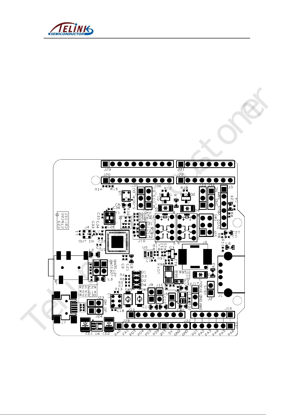
Figure 1 TLSR826XDK48 silkscreen
AN-18080300-E1 5 Ver 1.0.0

Telink TLSR826XDK48 User Guide
J29
1
10
J20
1
10
J31
1
8
J22
1
8
J3
1
6
J35
1
3
J34
1
3
J36
1 1 3
3
1
2
3
4
5
6
J25
J2
1
2
J1
J18
1
6
J21
1
6
J19
1
8
J28
1 6 1
4
J32
J7
J9
J11
1
2
1
2
J5
1
2
J17
1
3
J10
1
2
J23
1
2
J24
1
2
J33
S2
S2
4
3 2 1
6
8
1 9 5
7
J4
Telink for customer
Figure 2 TLSR826XDK48 photo
For schematic of TLSR826XDK48 board, please refer to Appendix or the PDF
document “C1T80A30_V2_0A”.
AN-18080300-E1 6 Ver 1.0.0

Telink TLSR826XDK48 User Guide
J1 USB Host
1
Connected to VBUS
2
Connected to TL_IO via 1K resistor
3
TL_SWM
4
GND
S1
GND
S2
GND
J7 mini USB interface (Power supply and debug)
1
VBUS
2
TL_DM
3
TL_DP
4~9
GND
J2
1~2
VBUS
J3 1 NC 2 TL_SWM
3
GND
4
VBUS
5
TL_SWS
6
TL_DVDD
J4 RF Connector
J5
1~2
VBUS/5V
J9
1~2
Connected to TL_DVDD and 3V3
J10 1 TL_32K01/C2
2
TL_32K02/C3
J11
1~2
TL_DVDD/TL_IO
J17 1 TL_3V3DUT
2
GND
3
TL_SWM
J18 & J21
1
TL_A6
2
TL_CN/P2N/A5
Telink for customer
2 EVK Pin Description
Table 1 EVK pin description
AN-18080300-E1 7 Ver 1.0.0

Telink TLSR826XDK48 User Guide
3
TL_CK/A4
4
TL_DI/A3
5
TL_DO/P0N/A2
6
TL_P2/D7
J19 1 NC 2 5V 3 TL_RST
4
3V3
5
5V 6 GND
7
GND
8
NC
J20 & J29
1
TL_I2CCK/C1
2
TL_I2CDI/C0
3
NC 4 GND
5
TL_CK/B7
6
DO 7 DI 8 TL_CN/B4
9
TL_D2
10
TL_D1
J22 & J31
1
TL_D0
2
TL_C7
3
AmicBias/C6
4
AmicSP/C5
5
AmicSN/C4
6
TL_B1
7
UTX
8
URX
J23
1~2
TL_DM/E2
J24
1~2
TL_DP/E3
J25 1 GND
2
TL_IO
3
TL_Row1
4
TL_Row0
Telink for customer
AN-18080300-E1 8 Ver 1.0.0

Telink TLSR826XDK48 User Guide
5
TL_Col1
6
TL_Col0
J28 1 TL_DDI/A0
2
TL_DCK/A1
3
TL_D3
4
TL_D4
5
TL_P0/D5
6
TL_P1/D6
J32 1 3V3
2
5V 3 GND
4
GND
J33 1 TL_UTX/B2
2
UTX
3
TL_URX/B3
J34 1 TL_URX/B3
2
URX
3
TL_UTX/B2
J35 1 TL_DO/B5
2
DO 3 TL_DI/B6
J36 1 TL_DI/B6
2
DI 3 TL_DO/B5
Telink for customer
AN-18080300-E1 9 Ver 1.0.0

Telink TLSR826XDK48 User Guide
J7
Option1:
1) Connect J9, J23 and J24 with Jumper Caps;
2) Connect J7 with PC USB via USB cable.
J9
J23
J24
1) Connect PIN3 with GND
Option 2: Connect J3 with
burning EVK
2) Connect PIN6 with 3.3V
3
6
J3
Telink for customer
3 Pin Connection Guide
3.1 Supply power for TLSR826XDK48
There are two connection methods to supply power for Telink TLSR826XDK48
board.
Method 1:
Make sure three jumper caps are connected on J9, J23 and J24 of
TLSR826XDK48.
Connect J7 (miniUSB interface) with PC USB via an USB cable.
Method 2:
Connect PIN3 and PIN6 of J3 with GND and 3.3V of a burning EVK, respectively.
AN-18080300-E1 10 Ver 1.0.0
Figure 3 Connection chart to supply power

Telink TLSR826XDK48 User Guide
J7
Option1:
1) Connect J9, J23 and J24 with Jumper Caps;
2) Connect J7 with burning EVK via USB cable.
J9
J23
J24
1) Connect PIN3 with GND
Option 2: Connect J3 with
burning key via Swire.
3) Connect PIN6 with 3.3V
3
6
J3
5
2) Connect PIN5 with SWM
Telink for customer
3.2 Download Firmware into TLSR826XDK48
There are two connection methods to download firmware into Telink
TLSR826XDK48 board.
1. Method 1: Connect via USB
Make sure three jumper caps are connected on J9, J23 and J24 of
TLSR826XDK48.
Connect J7 (miniUSB interface) with the USB interface of a burning EVK via an
USB cable. The miniUSB interface of the burning EVK is connected with PC USB
via an USB cable.
2. Method 2: Connect via Swire
Connect PIN3, PIN5 and PIN6 of J3 with GND, SWM and 3.3V of a burning EVK,
respectively.
Figure 4 Connection chart to download FW
AN-18080300-E1 11 Ver 1.0.0

Telink TLSR826XDK48 User Guide
Remove jumper cap from J9
J9
J3
3
6
Connect PIN3 with
3.3V power supply -
Connect PIN6 with
Amperemeter -
Telink for customer
3.3 Measure power-saving mode current for TLSR826XDK48
To measure current consumption of Telink TLSR826XDK48 board in deep sleep
or suspend mode, please follow the connection steps below:
1) Follow the steps in section 3.1 to download firmware into the TLSR826XDK48.
2) Power off the TLSR826XDK48.
3) Remove the jumper cap from J9 of TLSR826XDK48, as shown in Figure 5.
4) Connect anode (+) and cathode (-) of an amperemeter with anode (+) of 3.3V
power supply and PIN6 of J3, respectively.
5) Connect cathode (-) of the 3.3V power supply with PIN3 of J3.
AN-18080300-E1 12 Ver 1.0.0
Figure 5 Connection chart to test sleep current

Telink TLSR826XDK48 User Guide
Connect J4
Connect spectrum analyzer
J4
Connect J9, J23 and J24 with Jumper Caps.
J9
J23
J24
1) Connect PIN3 with GND
Option 2: Connect J3 with
burning key via Swire.
3) Connect PIN6 with 3.3V
3
6
J3
5
2) Connect PIN5 with SWM
Telink for customer
3.4 Test RF signal for TLSR826XDK48
Make sure three jumper caps are connected on J9, J23 and J24 of
TLSR826XDK48.
Connect PIN3, PIN5 and PIN6 of J3 with GND, SWM and 3.3V of a burning EVK,
respectively.
To test RF signal for Telink TLSR826XDK48 board, the J4 should be connected
with a spectrum analyzer via a RF cable (supplied by Telink).
AN-18080300-E1 13 Ver 1.0.0
Figure 6 Connection chart to test RF signal

Telink TLSR826XDK48 User Guide
Telink for customer
3.5 Test GPIOs for TLSR826XDK48
Since all GPIOs of Telink TLSR826XDK48 board are already connected to
corresponding pins of headers including J10, J21, J25, J28, J29, J31, J33, J34, J35 and
J36 (please refer to Table 1 or the schematic), user can directly test GPIO signals on
header pins.
FCC STATEMENT
This device complies with Part 15 of the FCC rules. Operation is subject to the
following two conditions: 1) this device may not cause harmful interference, and 2)
this device must accept any interference received, including interference that may
cause undesired operation.
This equipment has been tested and found to comply with the limits for a Class B
digital device, pursuant to Part 15 of the FCC rules. These limits are designed to
provide reasonable protection against harmful interference in a residential
installation. This equipment generates, uses and can radiate radio frequency energy
and if not installed and used in accordance with the instructions, may cause harmful
interference to radio communications. However, there is no guarantee that
interference will not occur in a particular installation. If this equipment does cause
harmful interference to radio or television reception, which can be determined by
turning the equipment off and on, the user is encouraged to try correct the
interference by one or more of the following measures:
- Reorient the receiving antenna.
- Increase the separation between the equipment and receiver.
- Connect the equipment into and outlet on a circuit different from that to
which the receiver is connected.
- Consult the dealer or an experienced radio/TV technician for help.
Changes or modifications not expressly approved by the party responsible for
compliance could void your authority to operate the equipment.
AN-18080300-E1 14 Ver 1.0.0
 Loading...