

Application Note:
Telink TLSR8232DK32 User
Guide
AN-17121200-E2
Ver 1.1.0
2018/1/26
TELINK SEMICONDUCTOR
Brief:
This document is the user guide for Telink TLSR8232DK32
board.
Telink for customer
Telink TLSR8232DK32 User Guide
Telink for customer
Published by
Telink Semiconductor
Bldg 3, 1500 Zuchongzhi Rd,
Zhangjiang Hi-Tech Park, Shanghai, China
© Telink Semiconductor
All Right Reserved
Legal Disclaimer
Telink Semiconductor reserves the right to make changes without further notice to
any products herein to improve reliability, function or design. Telink Semiconductor
disclaims any and all liability for any errors, inaccuracies or incompleteness contained
herein or in any other disclosure relating to any product.
Telink Semiconductor does not assume any liability arising out of the application or
use of any product or circuit described herein; neither does it convey any license
under its patent rights, nor the rights of others
The products shown herein are not designed for use in medical, life-saving, or lifesustaining applications. Customers using or selling Telink Semiconductor products not
expressly indicated for use in such applications do so entirely at their own risk and
agree to fully indemnify Telink Semiconductor for any damages arising or resulting
from such use or sale.
Information:
For further information on the technology, product and business term, please
contact Telink Semiconductor Company (www.telink-semi.com).
For sales or technical support, please send email to the address of:
telinkcnsales@telink-semi.com
telinkcnsupport@telink-semi.com
AN-17121200-E2 1 Ver 1.1.0
Version
Major Changes
Date
Author
1.0.0
Initial release
2017/12
T.J.B., Cynthia
1.1.0
Updated to C1T125A30_V1.1.
2018/1
T.J.B., Cynthia
Telink for customer
Revision History
Telink TLSR8232DK32 User Guide
AN-17121200-E2 2 Ver 1.1.0
Telink TLSR8232DK32 User Guide
Telink for customer
Table of contents
1 Brief......................................................................................................................... 4
1.1 Function ........................................................................................................... 4
2 Pin Description ........................................................................................................ 7
3 Pin Connection Guide ........................................................................................... 10
3.1 Supply power for TLSR8232DK32 .................................................................. 10
3.2 Download Firmware into TLSR8232DK32 ...................................................... 11
3.3 Measure power-saving mode current for TLSR8232DK32 ............................ 12
3.4 Test RF signal for TLSR8232DK32 ................................................................... 13
3.5 Test GPIOs for TLSR8232DK32 ....................................................................... 14
3.6 Arduino interface ........................................................................................... 14
4 Appendix ............................................................................................................... 15
Table of figures
Figure 1 TLSR8232DK32 silkscreen ...................................................................... 5
Figure 2 TLSR8232DK32 photo ............................................................................ 6
Figure 3 Connection chart to supply power ...................................................... 10
Figure 4 Connection chart to download FW ..................................................... 11
Figure 5 Connection chart to test sleep current ............................................... 12
Figure 6 Connection chart to test RF signal ....................................................... 13
Figure 7 Schematic of TLSR8232DK32 ............................................................... 16
Table of tables
Table 1 TLSR8232DK32 pin description.............................................................. 7
AN-17121200-E2 3 Ver 1.1.0
Telink TLSR8232DK32 User Guide
Telink for customer
1 Brief
This document presents guide on how to use Telink TLSR8232DK32 board, and
applies to all engineers who want to develop TLSR8232-based applications.
1.1 Function
Telink TLSR8232DK32 board can be used for SDK development. Firmware can be
directly downloaded to the TLSR8232DK32 board to be up and running.
Top view
AN-17121200-E2 4 Ver 1.1.0

Telink TLSR8232DK32 User Guide
Telink for customer
Bottom view
Figure 1 TLSR8232DK32 silkscreen
AN-17121200-E2 5 Ver 1.1.0

Telink TLSR8232DK32 User Guide
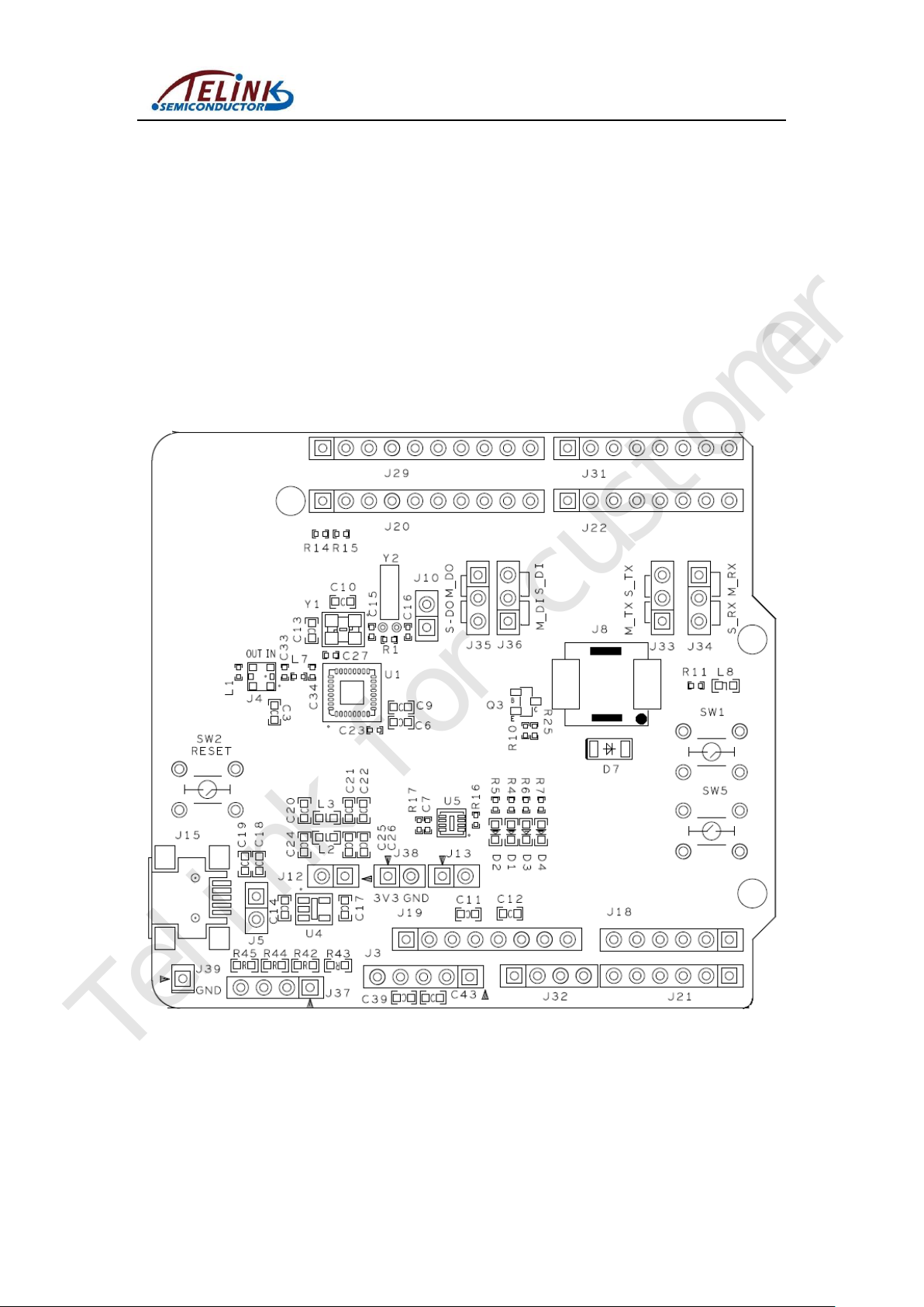
J29
1
10
J20
1
10
J31
1
8
J22
1
8
J35
J36
1
3
J10
1
2
J33
J34
1
1
3
3
J5
1
2
1
8
J19
J3
1
5
J32
1
4
J18
1
6
1
6
J15
J21
J4
1
2
7
9
8
6
1
5
1
3
J13
1
2
J38
1
2
J39
1
4
J37
Telink for customer
Figure 2 TLSR8232DK32 photo
For schematic of TLSR8232DK32 board, please refer to Appendix or the PDF
document “C1T125A30_V1.1”.
AN-17121200-E2 6 Ver 1.1.0

Telink TLSR8232DK32 User Guide
J3 1 NC 2 VBUS
3
DVDDIO
4
TL_SWS
5
GND
J4
RF Connector
J5
Connected to VBUS
J10
1
PB6
2
PB7
J12 & J13
Connected to 3V3
J15 mini USB interface (Power supply and debug)
1
VBUS
2
NC 3 TL_SWS
4~9
GND
J18 Arduino interface
1
ADC0/PB2
2
ADC1/PB1
3
ADC2/PB0
4
ADC3/PA7
5
ADC4/PA6
6
ADC5/PA5
J19 Arduino interface
1
NC 2 5V 3 RESET
4
3V3
5
5V 6 GND
7
GND
8
NC
J20 Arduino interface
1
SCL_PA3
2
SDA_PA4
Telink for customer
2 Pin Description
Table 1 TLSR8232DK32 pin description
AN-17121200-E2 7 Ver 1.1.0

Telink TLSR8232DK32 User Guide
3
NC 4 GND
5
SCK_PC5
6
MISO_PC4 (As Master) / MISO_PC3 (As Slave)
7
MOSI_PC3 (As Master) / MOSI_PC4 (As Slave)
8
SS_PC2
9
PC6
10
PC1
J21 1 PB2
2
PB1
3
PB0
4
PA7
5
PA6
6
PA5
J22 Arduino interface
1
PA0
2
PA1
3
PA2
4
PB3
5
NC 6 NC 7 URX_PB5 (As Master) / URX_PB4 (As Slave)
8
UTX_PB4 (As Master) / UTX_PB5 (As Slave)
J29 1 PA3
2
PA4
3
NC 4 GND
5
PC5
6
PC4
7
PC3
8
PC2
9
PC6
10
PC1
J31 1 PA0
2
PA1
3
PA2
4
PB3
5
NC
6
NC
Telink for customer
AN-17121200-E2 8 Ver 1.1.0

Telink TLSR8232DK32 User Guide
7
PB4
8
PB5
J32 1 3V3
2
5V 3 GND
4
GND
J33 UTX Jumper
J34 URX Jumper
J35 SPI_MOSI Jumper
J36
SPI_MISO Jumper
J37 1 100kohm external pull-up resistor
2
10kohm external pull-down resistor
3
1Mohm external pull-down resistor
4
50kohm external pull-down resistor
J38 1 3V3
2
GND
J39 GND
Telink for customer
AN-17121200-E2 9 Ver 1.1.0

Telink TLSR8232DK32 User Guide
J15
J12
Option1:
1) Connect J12 with Jumper Cap;
2) Connect J15 with PC USB via USB cable.
J3 3 5
1
2) Connect J3 PIN5 with GND
1) Connect J3 PIN3 with 3.3V
Optional 2:
1
2
Optional 3:
1) Connect J38 PIN1 with 3.3V
2) Connect J38 PIN2 with GND
J38
Telink for customer
3 Pin Connection Guide
3.1 Supply power for TLSR8232DK32
Three connection methods are supported to supply power for Telink
TLSR8232DK32 board.
1. Method 1:
Make sure a jumper cap is connected on J12 of TLSR8232DK32.
Then connect J15 (miniUSB interface) with PC USB via an USB cable.
2. Method 2: Connect PIN3 and PIN5 of J3 with 3.3V and GND, respectively.
3. Method 3: Connect PIN1 and PIN2 of J38 with 3.3V and GND, respectively.
Figure 3 Connection chart to supply power
AN-17121200-E2 10 Ver 1.1.0

Telink TLSR8232DK32 User Guide
J15
J12
Option1:
1) Connect J12 with Jumper Cap;
2) Connect J15 with burning key via USB cable.
J3
3
5
1
Option2: Connect J3 with burning key
1) Connect PIN3 with 3.3V
2) Connect PIN4 with SWM
3) Connect PIN5 with GND
4
Telink for customer
3.2 Download Firmware into TLSR8232DK32
Two connection methods are supported to download firmware into Telink
TLSR8232DK32 board.
1. Method 1: Connect via USB
Make sure a jumper cap is connected on J12 of TLSR8232DK32.
Connect J15 (miniUSB interface) with the USB interface of a burning key (i.e.
burning EVK board) via an USB cable. The miniUSB interface of the burning key is
connected with PC USB via an USB cable.
2. Method 2: Connect via Swire
Connect PIN3, PIN4 and PIN5 of J3 with 3.3V, SWM and GND of a burning key,
respectively.
Figure 4 Connection chart to download FW
AN-17121200-E2 11 Ver 1.1.0

Telink TLSR8232DK32 User Guide
J12
Remove jumper cap from J12
Remove jumper cap from J13
J3
5
Connect J12 PIN2 with Amperemeter -
Connect J3 PIN5 with 3.3V power supply -
J13 1 2
Telink for customer
3.3 Measure power-saving mode current for TLSR8232DK32
To measure current consumption of Telink TLSR8232DK32 board in deep sleep or
suspend mode, please follow the connection steps below:
1) Remove jumper caps from J12 and J13 of TLSR8232DK32.
2) Connect anode (+) and cathode (-) of an amperemeter with anode (+) of 3.3V
power supply and PIN2 of J12, respectively.
3) Connect cathode (-) of the 3.3V power supply with PIN5 of J3.
AN-17121200-E2 12 Ver 1.1.0
Figure 5 Connection chart to test sleep current

Telink TLSR8232DK32 User Guide
Connect J4
Connect spectrum analyzer
J4
Telink for customer
3.4 Test RF signal for TLSR8232DK32
To test RF signal for Telink TLSR8232DK32 board, the J4 should be connected with
a spectrum analyzer via a RF cable (supplied by Telink).
AN-17121200-E2 13 Ver 1.1.0
Figure 6 Connection chart to test RF signal

Telink TLSR8232DK32 User Guide
Telink for customer
3.5 Test GPIOs for TLSR8232DK32
Since all GPIOs of Telink TLSR8232DK32 board are already connected to
corresponding pins of headers including J3, J10 (if PB6 and PB7 are not used as external
32kHz crystal output and input), J21, J29 and J31 (please refer to Table 1 or the
schematic), user can directly test GPIO signals on header pins.
3.6 Arduino interface
Telink TLSR8232DK32 board is compatible with Arduino standard interface,
which adopts single-column direct-in female headers (J18, J19, J20, J22) with pin
distance of 2.54mm. The TLSR8232DK32 can be used for development in the
following two cases:
1) By default, the TLSR8232DK32 acts as Host control board by connecting it with
Arduino shield daughter board. In this case, it’s needed to connect four jumper
caps with PIN1 and PIN2 of J33, PIN1 and PIN2 of J34, PIN1 and PIN2 of J35, as
well as PIN1 and PIN2 of J36.
2) The TLSR8232DK32 can also act as Arduino shield daughter board in
combination with Arduino Host control board. In this case, it’s needed to
connect four jumper caps with PIN2 and PIN3 of J33, PIN2 and PIN3 of J34, PIN2
and PIN3 of J35, as well as PIN2 and PIN3 of J36.
FCC statement:
This device complies with Part 15 of the FCC rules. Operation is subject to the following two conditions: 1)
this device may not cause harmful interference, and 2) this device must accept any interference received,
including interference that may cause undesired operation.
Changes or modifications not expressly approved by the party responsible for compliance could void your
authority to operate the equipment.
AN-17121200-E2 14 Ver 1.1.0
 Loading...