

Page 1
1505 Audio Line Driver
CH 1
CH 1
Tx
Rx
MIC
SPEAKER
CH 2
CH 2
CH 3
CH 3
CH 4
CH 4
Service Manual
1505 M IXER/
LINE DRIVER
CH 1
CH 2
MUTE
CH 3
CH 4
SPKR
PTT
HANDSET
MIC
SPEAKER
CH 1
CH 2
Tx
CH 3
CH 4
CH 1
CH 2
Rx
CH 3
CH 4
LEVEL ADJUST
098-0355
Page 2

Table of Contents
1. General ........................................................1
2. Standard Features ................................................1
3. Installation ......................................................1
4. Connections .....................................................3
5. Operation .......................................................5
6. Theory of Operation ..............................................7
7. 1505 Specifications ...............................................10
8. Parts List ......................................................11
1. General
The Vega Model 1505 Audio Line Driver is a
general purpose card that provides a reliable
means of remotely controlling a variety of cus
tomer specified devices. The card is flexible. It
can perform basic switching functions, custom
ized switching functions (via jumpers), or spe
cial user-defined functions. It plugs into a
Tellabs Type 10 or equivalent open frame rack
and can be used in conjunction with any remote control console.
2. Standard Features
•
Four balanced line inputs, switchable
•
Four single-ended inputs, switchable
•
One microphone input from front panel or
connector
•
Jumper options for carbon, electret, or dy
namic microphone elements
•
Four balanced 600-ohm line outputs
•
One-watt eight-ohm speaker output
•
12 Vdc operation
•
All receive inputs can be individually muted
by rear panel switch low inputs
2.1 Optional Features include:
•
Jumper-selected receive input compression
•
User switch-programmable mixing function,
for example one input can be switched to
any or all outputs
•
Jumper selectable 600 ohm or 10K ohm high
input impedance
3. Installation
Caution - ESD Sensitive
-
This piece of electronic equipment con
-
tains electronic components known to be
-
-
susceptible to Electro-Static Discharge
(ESD). Precautions have been taken to
avoid the effects of ESD, however the user
is encouraged to promote safe handling
techniques in the handling, storage and
service of this equipment.
3.1 Introduction
Only experienced technicians familiar with
similar types of equipment should attempt to
install the 1505. Only basic hand tools are required to remove the card, change jumper set-
-
tings, connect phone, signal, and power lines.
Read this section thoroughly before attempting
to install the card. Exercise care to prevent wir
-
ing errors and equipment damage.
3.2 Inspection
Carefully unpack the equipment and inspect it
thoroughly as soon as possible after delivery. If
any part of the equipment has been damaged in
shipment, report the extent of the damage to
the transportation company immediately.
This unit has been inspected and adjusted to its
recommended operation condition at the fac
tory. Unless it has been handled roughly in
shipment, abused or tampered with, it won’t re
quire further adjustments. Simply make the in
stallation connections as described in the fol
-
-
lowing sections.
1
Page 3
3.3 Mounting
This card is intended to be mounted in a
Tellabs Type 10 or equivalent open frame rack.
To avert erroneous operation, don’t install the
card adjacent to equipment that generates high
temperature or electromagnetic radiation. Al
ways provide an appropriate service loop on in
terconnecting cables.
3.4 Access for Installation/Servicing
When installing into a Tellabs Type 10 or
equivalent open frame rack, ensure the front
and rear of the rack have clear access for card
installation and wiring.
-
-
To service, remove the 1505 from the rack or
place on a circuit card extension for access
while troubleshooting.
3.5 Power
Primary power for the card is a regulated
source of 12 Vdc.
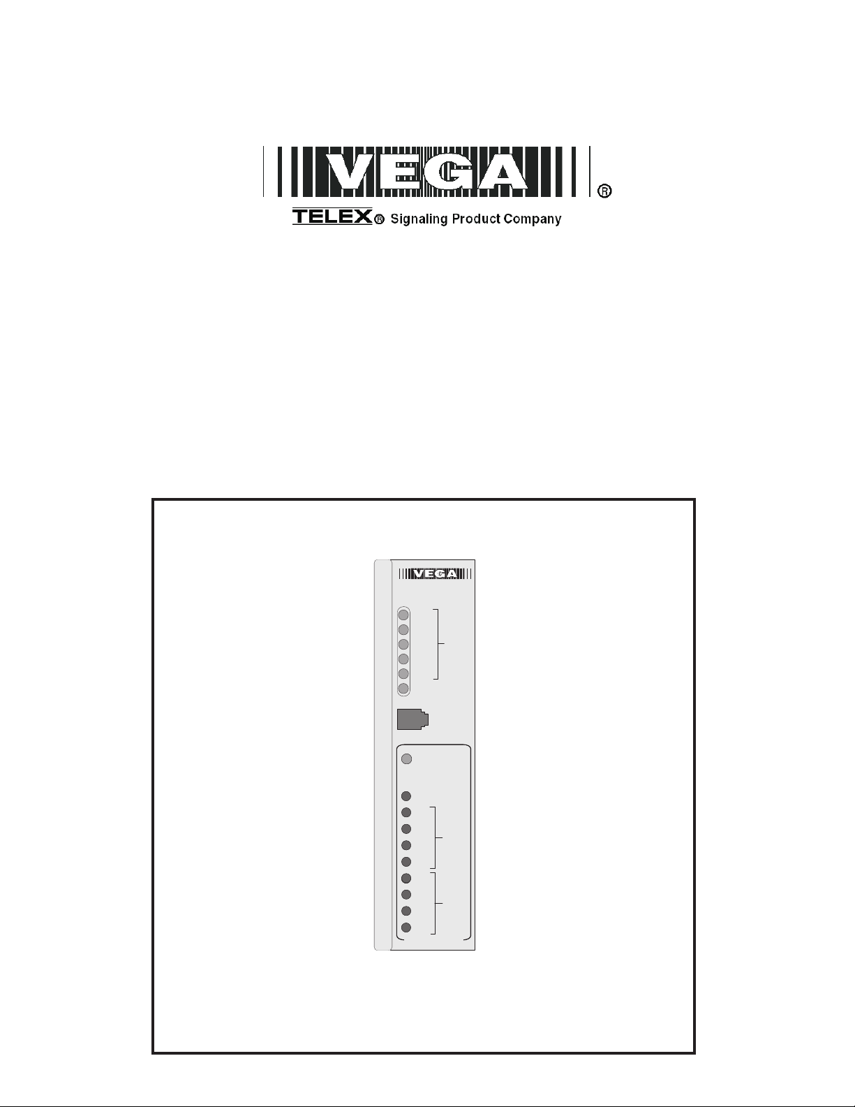
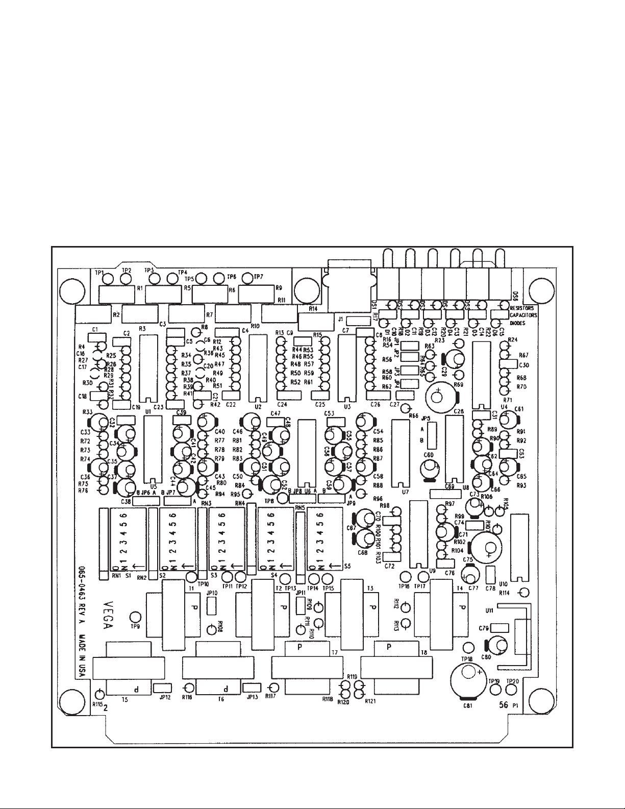
Figure 1. 1505 Component Location
2
Page 4

4. Connections
Warning - High Voltage! Remove
Power Before Servicing!
High voltage may be present on this card (if
used for switching phone lines with super
imposed dc current signaling) which could
cause serious injury or loss of life. Only
qualified personnel familiar with this type
of circuitry should work on this equipment.
To prevent injury, damaging the card or
other equipment, remove power before
making connections.
4.1 Power connections
Connect positive 12 Vdc to pins 55 and 56.
Connect the 12 Vdc return (normally ground)
to pins 39 and 40. For best performance, use at
least 20 AWG or larger wire for power connections.
4.2 Signal Connections and Card Edge Con
nector Pin Assignment
Refer to the schematic and Table 4 (shows the
1505’s pin assignments and has a blank for any
-
customized functions that might be configured)
for the appropriate pin number to make connec
tions. Use at least 24 AWG wire for signal
connections.
4.3 Special considerations for optional wiring
4.3.1 Receive Compressor/Limiter Jumpers
Each receive channel has a compressor/limiter
circuit which helps provide a consistent audio
level. If some external equipment already in
cludes compressor/limiters, these circuits may
be bypassed by changing the associated
jumper’s position. For example, moving JP6
from the “A” (in) to the “B” position (out) bypasses Rx Ch #1’s Compressor/Limiter. Refer
to Table 1 and the schematic for the appropriate jumper selection.
JP# Function Jumper Status Notes
In Out A B
1 Mic PTT/Speaker Mute Coupled Separate N/A N/A PTT mutes Speaker
2 Mic, Carbon Element In - N/A N/A
3 Mic, Electret Element In - N/A N/A
N/A Mic, Dynamic, High Out - - N/A N/A JP2, 3, 4 out
4 Mic, Dynamic, Low Out In - N/A N/A
5 Mic, Comp./Lim. N/A N/A In Bypass
6 Rx Ch #1 Comp./Lim. N/A N/A In Bypass
7 Rx Ch #2 Comp./Lim. N/A N/A In Bypass
8 Rx Ch #4 Comp./Lim. N/A N/A In Bypass
9 Rx Ch #3 Comp./Lim. N/A N/A In Bypass
10 RX Ch #3 600Ω/10ΚΩ 600Ω 10ΚΩ Ν/Α Ν/Α
11 RX Ch #1 600Ω/10ΚΩ 600Ω 10ΚΩ Ν/Α Ν/Α
12 RX Ch #4 600Ω/10ΚΩ 600Ω 10ΚΩ Ν/Α Ν/Α
13 RX Ch #2 600Ω/10ΚΩ 600Ω 10ΚΩ Ν/Α Ν/Α
Table 1. Jumper Options
3
Page 5

4.3.2 Microphone Jumpers
Depending on which microphone you are us
ing, the following jumpers must be installed:
JP2 - carbon element; JP3 - electret element;
JP4 - dynamic element with a low output.
No jumpers are installed for a dynamic micro
phone with a high output.
4.3.3 Receive Line Input Impedance
A 600Ω terminating resistor is provided for
each receive line input. Refer to the schematic
and Table 1 for the proper jumper installation.
4.3.5 Parallel Transmit Line Impedance
-
Matching
If the occasion arises where the transmit line
output must operate in parallel with another
line terminating device, an impedance mis
match to the phone line will result. To maintain
ate a resistive pad on the output of the 1505
a 600Ω termination, it will be necessary to cre
-
line driver. A similar pad must be installed in
each parallel device. This resistive pad creates
a matching network with the phone line, how
ever it induces a loss in the transmission path
which lowers the line level and may affect the
ultimate performance.
4.3.4 Switch Settings
Switches S1 to S5 provide the means to pro
gram the signal inputs to the output circuits.
Any input can be programmed to any output.
Multiple inputs can be combined to a single
output, or conversely a single input can be programmed to one output. Refer to the schematic
and Table 2 for the proper jumper installation.
Refer to the schematic and Table 2 for proper
switch closures.
-
In order to easily insert the pad, a provision has
been made in the circuit to allow the user to al
ter the value of two resistors in the transmit
line output. The 1505 is shipped from the fac
tory for single line termination without a pad,
resulting in the balanced transmit line output
having a 0 Ω resistor in each leg of the transformer without loss. To add the pad, both 0 Ω
resistors must be replaced with a value corresponding to the number of parallel lines. Refer
to the schematic and Table 3 for proper resistor
values and corresponding insertion loss.
Table 2. Output Programming Switch Settings/Associated Switch
Input Outputs
Tx Ch #1 Tx Ch #2 Tx Ch #3 Tx Ch #4 Speaker
Rx Ch #1 S-1 S-1 S-1 S-1 S-1
Rx Ch #2 S-2 S-2 S-2 S-2 S-2
Rx Ch #3 S-3 S-3 S-3 S-3 S-3
Rx Ch #4 S-4 S-4 S-4 S-4 S-4
-
-
Mic Input S-5 S-5 S-5 S-5 S-5
Sum Audio In S-6 S-6 S-6 S-6 S-6
Table 3. Parallel Transmit Line Resistor Network Selection
Tx Ch # Resistor Designation Parallel Lines, Resistor Value / Line Loss (dB)
234
1 R112, R113 300 Ω/6dB 620 Ω / 9.5 dΒ 910 Ω / 12.0 dΒ
2 R119, R121 300 Ω/6dB 620 Ω / 9.5 dΒ 910 Ω / 12.0 dΒ
3 R109, R110 300 Ω/6dB 620 Ω / 9.5 dΒ 910 Ω / 12.0 dΒ
4 R118, R120 300 Ω/6dB 620 Ω / 9.5 dΒ 910 Ω / 12.0 dΒ
4
Page 6

4.4 Securing the Connections
After all power and line connections are made,
the wires should be neatly bundled and secured
in place to prevent accidental breakage when in
service. Use one or more of the cable guides
supplied with the card rack, or tie in place with
appropriate wire ties.
4.5 Interface connector Numbering
The Tellabs (or equivalent) card cage interface
connector pins may have a different numbering
scheme than the 1505. Table 4 depicts the card
edge pin numbers as shown in the schematic,
which is also the same as one type of connec
tor, followed by two alternate numbering
schemes as used on other connectors. Dili
gently review the actual connections being
used, to Table 4, to ensure proper connections
are made for optimum performance. Record the
external connections made during installation in
the blanks rows in Table 4’s “User Connection” column (make copies of Table 4 and keep
records for each 1505).
5. Operation
5.1 Description
This 1505 module has up to four, receive balanced 600 Ω line inputs or high impedance un-
balanced inputs, along with a Mic/Handset input, that is user configurable by dip switch set-
ting, to drive from one to four 600 Ω balanced
transmit line outputs, or an 8 Ω remote speaker.
The module is also capable of summing up to
four receive channel inputs and/or a Mic/Hand
set input, into one or more transmit line outputs
or the speaker output.
5.2 Operating Capabilities
The 1505 accepts up to four balanced or unbal
anced inputs, switch selectable by the user, to
four balanced line driver outputs. These inputs
are also externally mutable by switched low in
puts at the rear panel connection. In addition,
the module will accept a microphone or hand
set input through the front panel jack or the
rear panel connector.
The transmit amplifier is a 600-ohm balanced
line output. The module has four balanced line
outputs. Each amplifier output is adjustable
-
-
with a range of -15 to 10 dBm.
The module has a speaker amplifier output that
may drive an eight ohm external speaker with
an output level of 1 watt. The level is adjust
able.
Any line or microphone input may be switched
(through a module dip switch) to any line output or the speaker output. Three 1505s can be
connected so one line input may drive up to
twelve 600-ohm line outputs. Each input is mutable and the control is a switched low on the
rear panel connector. A PTT from the microphone or handset will gate on the microphone
amplifier and is also jumper selectable to mute
the speaker to inhibit crosstalk.
5.3 Controls and Indicators
Front panel LEDs light when the corresponding
-
receive channel or speaker is muted and when
the microphone or handset PTT switch is acti
vated.
A compressor/limiter circuit is available by
jumper selection for each receive circuit, to
limit the input level to a predetermined setting,
which assists in maintaining proper system lev
els. This module also contains a summed input
circuit, and a summed output circuit, to allow it
to be used in a matrix, i.e. three modules can
be configured to allow a single input to drive
twelve outputs, or conversely twelve inputs can
be summed to one output.
Active switch input circuits allow for muting
individual receive input channels, or the
speaker. A PTT input activates the microphone
circuit.
-
5
Page 7

Table 4. Card Edge Connector Pin Assignments (Solder Side)
Card Alt #1 Alt #2 Function User Connection
Edge Conn Conn
1 A A Ch #4 Rx Bal. Line In (-)
3 B B Ch #4 Rx Mute
5 C C Ch #4 Rx Bal. Line In (+)
7 D D Ch #4 Rx UnBal Line In
9 E E Ch #3 Rx UnBal Line In
11 F F Ch #3 Rx Bal Line In (+)
13 H H Ch #3 Rx Bal. Line In (-)
15 J J Ch #2 Rx Bal. Line In (-)
17 K K Ch #3 Rx Mute
19 L L Ch #2 Rx UnBal Line In
21 M M Ch #2 Rx Bal Line In (+)
23 N N Ch #2 Rx Mute
25 P P Ch #1 Rx Unbal Line In
27 R R Ch #1 Rx Bal Line In (+)
29 S S Ch #1 Rx Bal. Line In (-)
31 T T Ch #1 Rx Mute
33 U U Ch #4 Tx Bal. Line Out (+)
35 V V Ch #3 Tx Bal. Line Out (+)
37 W W Ch #2 Tx Bal. Line Out (+)
39 X X Pos. 12 Vdc Return (Gnd)
41 Y Y Ch #1 Tx Bal. Line Out (+)
43 Z Z No Connection
45 A AA Sum Audio Out
47 B BB Mic Audio In
49 C CC Mic PTT
51 D DD N/A
53 E EE No Connection
55
F FF Position 12 Vdc Input
(Component Side)
Card Alt #1 Alt #2 Function User Connection
Edge Conn Conn
2 1 1 No Connection
4 2 2 Ch #4 RXAGND
6 3 3 Ch #4 Mute Gnd
8 4 4 No Connection
10 5 5 No Connection
12 6 6 Ch #3 RXAGND
14 7 7 Ch #3 Mute Gnd
16 8 8 No Connection
18 9 9 No Connection
20 10 10 Ch #2 RXAGND
22 11 11 Ch #2 Mute Gnd
24 12 12 No Connection
26 13 13 No Connection
28 14 14 Ch #1 RXAGND
30 15 15 Ch #1 Mute Gnd
32 16 16 No Connection
34 17 17 Ch #4 Tx Bal. Line Out (-)
36 18 18 Ch #3 Tx Bal. Line Out (-)
38 19 19 Ch #2 Tx Bal. Line Out (-)
40 20 20 Pos. 12 Vdc Return (Gnd)
42 21 21 Ch #1 Tx Bal. Line Out (-)
44 22 22 Sum Audio In
46 23 23 Earpiece Audio Out
48 24 24 Speaker Mute
50 25 25 MICAGND
52 26 26 No Connection
54 27 27 N/A
56 28 28 Pos. 12 Vdc Input
6
Page 8

6. Theory of Operation
6.1 General
The 1505 module uses a low loss, wide band
transformer for each channel to interface to the
phone line. Gain elements are low noise, low
distortion, high gain operational amplifiers for
quality performance. Each channel utilizes one
half of dual compandor IC, configured as a
compressor/limiter, to amplify and limit the
maximum receive input signal, in order to
maintain operator adjusted system levels.
Each receive amplifier output is routed through
a user programmed switch matrix, to summing
amplifiers. The output of the summing amplifi
ers are transmit line amplifiers, and a low loss,
wide band transformer for each channel to in
terface to the respective phone line.
A handset/microphone amplifier circuit is included, with provision for jumper selection of
carbon, electret, or dynamic microphone elements. Also included is a compressor/limiter
circuit to maintain system levels. The output of
the handset/microphone amplifier circuit is
routed to the switch matrix.
An on board voltage regulator maintains proper
voltages for optimum performance.
6.2 Receive Amplifier
This amplifier is a jumper-selectable, 600 ohm
or 10k ohm, high impedance balanced input
that is adjustable from a range of -30 dBm to
10 dBm.
Each receive amplifier has an unbalanced input
with an input level of 0.025 Vac to 2.5 Vac
each. The amplifier output is adjustable and is
accessed through the front panel. The output
level for each receive amplifier is normally
setup for a level of 0.776 Vrms at the test
point. For example, channel one’s test point is
TP3. Operation is the same for all four receive
inputs.
6.3 Compression Limiter Circuit
This circuit amplifies and limits the output of
the receive inputs ensuring uniform audio lev
els from all channels regardless of the input
level received from the external line input. For
a 30 dB gain, once achieving the compression
level, onlya3dBincrease in output level,
without distortion, results in the circuit.
Normally the input level, at 0 dB, allows the
limiter to amplify in a linear fashion below that
level, and above the 0.776 will limit the output
to no more than a 3 dB rise above that point. A
jumper allows the bypass of the compressor
circuit. The compressor circuit is the same for
all four receive channel circuits. Each receive
-
-
input can be muted by an external switched
low input from the rear panel. A front panel
LED mute indicator alerts the operator that the
channel is muted. The output from each receive
channel is bussed through various switches and
is switch selectable by the user to have the audio appear at any one of four line outputs or a
speaker output.
6.4 Transmit Line Amplifier
This bridging amplifier drives a 600 ohm balanced line with an output level adjustable from
-15 dBm to 10 dBm. The output level is adjustable through the front panel. Each transmit amplifier is also a mixer which allows the mixing
of any one or all four receive channels mixed
into one transmit line amplifier.
-
NOTE
The speaker amplifier circuit is no longer
useable, the IC required to drive this cir
cuit has been obsolete by the manufacture
and there is no substitute being manufac
tured at this time. Should you have any
quiestions regarding the speaker amplifier
circuit please call: 1-800-752-7560 Ext
291 for further informaion;
-
-
7
Page 9

Page 10

Page 11

8
Page 12

6.5 Microphone Input
A microphone input is available through a jack
on the front panel. It allows connection of a
handset or palm type microphone through a
standard modular phone connection. The
jumper options allow the use of a carbon,
electret, or dynamic element. The microphone
amplifier is adjustable to accommodate the full
range of microphones. It’s routed through a
compression limiter similar to the receiver cir
cuits. This compressor operates in a linear fash
ion below 0.776 Vrms input or will have a
limit of 3 dBm increase if that level is ex
ceeded. This limiter may also be bypassed by a
jumper selection. The output of the microphone
circuits is normally muted and is gated on by
the PTT switched in the handset or micro
phone. A jumper is available to simultaneously
mute the speaker during the time the PTT is
initiated so that audio feedback is eliminated.
The output of the microphone circuit is bussed
though switches to the transmit line output amplifiers and to the speaker amplifier output so
that the user may select which line or the
speaker that the microphone input circuit can
be applied to.
6.6 Sum Audio
The 1505 has a sum audio input circuit and a
sum audio output circuit which allows matrix
operation with several modules. This allows the
expansion of receive input channels or transmit
line channels. For example, using three 1505s,
one receive input channel can be
switch-selected for up to twelve channels out
put or conversely twelve receive channels may
be mixed into one transmit channel.
6.7 Controls
Each receive input and microphone input can
be muted externally from the rear panel by a
switched low input, this allows remote muting
by an external source of the various inputs. A
PTT unmutes the microphone audio amplifier
by the PTT switch on the handset or the micro
phone. This PTT is also routed to the rear con
nector panel and is activated by a switched low
input.
6.8 Indicators
The speaker and each receive input channel can
be muted. The front panel has an indicator to
visibly indicate which channels have been
muted. The front panel also has a PTT LED
which is illuminated when the PTT switch has
been activated on the handset or microphone.
6.9 Power Supply
-
-
The 1505 is intended for operation with a 12
Vdc semi-regulated power supply. The onboard
regulator limits the input voltage and regulates
-
the output voltages to operate the module under
various input voltages. The power supply is
fixed and non-adjustable. The regulator safely
limits the output current through the module.
-
Reverse input protection is also provided in
case of an inadvertent reverse voltage input.
Warranty (Limited)
All Vega signaling products are guaranteed
against malfunction due to defects in materials
and workmanship for three years, beginning at
the date of original purchase. If such a malfunction occurs, the product will be repaired or
replaced (at our option) without charge during
the three-year period, if delivered to the Vega
factory. Warranty does not extend to damage
due to improper repairs, finish or appearance
items, or malfunction due to abuse or operation
under other than the specified conditions, nor
does it extend to incidental or consequential
damages. Some states do not allow the exclu
-
sion or limitation of incidental or consequential
-
damages, so the above limitation may not apply
to you. This warranty gives the customer spe
cific legal rights, and there may be other rights
which vary from state to state.
-
-
9
Page 13

7.
1505 Specifications
Operating Temperature Range: ..................................0°Cto60°C
Power Requirements: .............................11to16V
rms semi-regulated,
250 mA nominal 600 Ω/10K Ω
Balanced Receive Line Input Level: ....-30dBmto+10dBm,adjustable 10 K Ω/10 K Ω
Unbalanced Receive Input Level: .....0.025 V
Mic Input Sensitivity: ...............0.010 V
Summing Input Level: .............................0dBm(0.776 V
rms to 2.5 Vrms, adjustable 10 K Ω/10K Ω
rms to 1.0 Vrms, adjustable 10K Ω/10K Ω
rms) nominal
Receive Amplifier Distortion:...................................1%THDmax.
Receive Frequency Response: ........................+1/-2 dB, 100 Hz to 10 KHz
Compression Range: ..........30dBincrease in signal, output increases less than 3 dB
Summing Level: ..................................0dBm(0.776 V
rms) nominal
Balanced Transmit Line Output Level: ............-15dBmto+10dBm,600Ω Line
Transmit Amplifier Distortion: .........................1%THDmax.@0dBm
Transmit Frequency Response: .......................+1/-2 dB, 100 Hz to 10KHz
Summing Amplifier Output Level: ....................0dBm(0.776 V
rms) nominal
Summing Amplifier Distortion: .........................1%THDmax.@0dBm
Summing Amplifier Frequency Response: ..............+1/-2 dB, 100 Hz to 10 KHz
Crosstalk Line to Line: .........................................-55dBmin.
S/N @ -10 dBm Input: ..........................................-65dBmin.
10
Page 14

8.
1505 Parts List
Part No. Description Ckt
Sym
Part No. Description Ckt
Sym
012-0085 PCB SUB ASSY 1505MIX/LINE
031-0226 TEXT SPEC 1505 AUD MIX/LD
065-0463 PCB 1505 AUD MIX/LIN DR
071-0566 SCHEMATIC 1505 MIX/LINE D REF
102-0120 CAP CER 20P 5% 50V S2L C2
C5
C19
C23
102-0290 CAP CER100P S2L 5% 50V C8
C9
C22
C25
C76
102-0400 CAP CER 330P S2L 5% 50V C4
C7
C24
C26
102-0420 CAP CER 390P S2L 5% 50V C69
103-0001 CAP CER.001 10% 50V Y5P C31
C32
C39
C47
C53
104-0767 CAP TANT 1UF 35V C6
C16
C17
C20
110-1340 CAP CER .1MF SMALL C1
C3
C10
C11
C12
C13
C14
C15
C18
C21
C27
C30
C63
C70
C72
C74
C78
C79
112-1606 CAP ELEC 10MF 25V C37
C44
C51
C57
C66
C77
112-1608 CAP ELEC 1.0MF 20% 25V C33
C34
C35
C36
C40
C41
C42
C43
C46
C48
C49
C50
C54
C55
C56
C58
C61
C62
C64
C65
112-1609 CAP ELEC 100MF 20% 25V C28
112-1645 CAP ELEC 4.7UF 25V MINI C29
C38
C45
C52
C59
C60
C71
112-1671 CAP ELEC 22 UF 25V 10%RD C73
112-1675 CAP ELEC 10UF 16V RAD C67
C68
C80
112-1689 CAP ELEC 470 MF25V RAD C81
112-1691 CAP ELEC 220UF 25V C75
130-0777 RES VAR 1.0K LOG CERMET R11
130-0778 RES VAR 10K LOG CERMET R14
130-0779 RES VAR 50K LOG CERMET R6
R7
R9
R10
130-0780 RES VAR 500K LOG CERMET R1
R2
R3
R5
132-0009 RES 1/4W ZERO-OHM JUMPER R66
R71
R109
R110
R112
R113
R114
R117
R118
R119
R120
R121
11
Page 15

Part No. Description Ckt
Sym
Part No. Description Ckt
Sym
134-2837 RES RN55D 15.0K 1% 1/4W R100
R103
134-2967 RES RN55D 12.1K 1% 1/4W R98
134-3032 RES RN55D 15.8K 1% 1/4W R101
136-0001 RES COMP 2.7 5% 1/4W R107
136-0022 RES COMP 150 5% 1/4W R63
136-0040 RES COMP 4.7K 5% 1/4W R99
136-0044 RES COMP 10K 5% 1/4W R13
R16
R24
R26
R27
R30
R31
R35
R36
R39
R40
R46
R47
R51
R56
R57
R61
R68
R75
R79
R83
R87
R92
136-0050 RES COMP 33K 5% 1/4W R4
R8
R33
R42
R72
R73
R77
R78
R81
R82
R85
R86
R89
R90
R91
136-0056 RES COMP 100K 5% 1/4W R23
R65
R70
R76
R94
R95
R96
136-0060 RES COMP 220K 5% 1/4W R74
R80
R84
R88
R93
136-0090 RES COMP 650 5% 1/4W R12
R15
R17
R18
R19
R20
R21
R22
R52
R62
R67
R105
R106
R108
R111
R115
R116
136-0096 RES COMP 2K 5% 1/4W R25
R32
R34
R41
R43
R50
R53
R60
136-0289 RES COMP 200K 5% 1/4W R104
136-1765 RES COMP 3K 5% 1/4W R69
136-1955 RES COMP 5.1K 5% 1/4W R28
R29
R37
R38
R44
R45
R48
R49
R54
R55
R58
R59
R97
R102
136-1983 RES COMP 9.1K 5% 1/4W R64
138-0029 RNET CMN 7X10K SIP RN1
RN2
RN3
RN4
RN5
161-0426 DIODE 1N4148 D1
D2
D3
D4
D5
D6
161-0630 LED PCB RDT1 ¾ D1F RED DS1
161-0631 LED PCB YLT1 ¾ D1F YEL DS2-6
12
Page 16

Part No. Description Ckt
Sym
Part No. Description Ckt
Sym
286-1766 CONN JUMPER PLUG JP1
JP2
JP3
JP4
JP5
JP6
JP7
JP8
JP9
JP10
JP11
JP12
JP13
286-1772 CONNECTOR 36PIN STRIP TIN JP1
JP2
JP3
JP4
JP5
JP6
JP7
JP8
JP9
JP10
JP11
JP12
JP13
286-1964 TEST POINT YELLOW .055 MNT TP1
TP2
TP3
TP4
TP5
TP6
TP7
TP8
TP9
TP10
TP11
TP12
TP13
TP14
TP15
TP16
TP17
TP18
TP19
TP20
286-2011 CONN PCB MODULAR 4PIN HS J1
299-0303 SWITCH 6PST DIP S1
S2
S3
S4
S5
318-0246 XFORMER 10K CT-10K CT T1
T2
T5
T6
318-0259 XFORMER 600CT-600CT T3
T4
T7
T8
425-0178 INT CKT NE570N U5
U6
U8
425-0210 IC OPAMP LM348 QUAD U1
U9
425-0488 OPAMP QUAD LMC660 OV INP U2
U3
425-0529 IC CMOS SW DG212B 4XSPST U4
U7
425-0530 IC LM2937 ET-10 VOLT REG U11
534-0001 SCREW PH 4-40X1/4 NYLOK
538-0075 NUT KEP 4-40
614-0434 HEAT SINK TO-220 21C/W
13
Page 17

8601 East Cornhusker Highway, Lincoln, Nebraska, 68507
NOV. 2000 Printed in U.S.A.
Phone: (402) 467-5321 / (800) 752-7560 Fax: (402) 467-3279
E-mail: vega @telex.com, Web: www.vega-signaling.com
 Loading...