

Page 1

SSEERRVVIICCEE MMAANNUUAALL
SSEERRVVIICCEE MMAANNUUAALL
SSEERRVVIICCEE MMAANNUUAALL
SSEERRVVIICCEE MMAANNUUAALL
SSEERRVVIICCEE MMAANNUUAALL
SSEERRVVIICCEE MMAANNUUAALL
SSEERRVVIICCEE MMAANNUUAALL
SSEERRVVIICCEE MMAANNUUAALL
SSEERRVVIICCEE MMAANNUUAALL
SSEERRVVIICCEE MMAANNUUAALL
SSEERRVVIICCEE MMAANNUUAALL
SSEERRVVIICCEE MMAANNUUAALL
SSEERRVVIICCEE MMAANNUUAALL
SSEERRVVIICCEE MMAANNUUAALL
SSEERRVVIICCEE MMAANNUUAALL
SSEERRVVIICCEE MMAANNUUAALL
SSEERRVVIICCEE MMAANNUUAALL
SSEERRVVIICCEE MMAANNUUAALL
SSEERRVVIICCEE MMAANNUUAALL
SSEERRVVIICCEE MMAANNUUAALL
SSEERRVVIICCEE MMAANNUUAALL
SSEERRVVIICCEE MMAANNUUAALL
PT-90
NEAT
CHASSIS
SSEERRVVIICCEE MMAANNUUAALL
SSEERRVVIICCEE MMAANNUUAALL
SSEERRVVIICCEE MMAANNUUAALL
SSEERRVVIICCEE MMAANNUUAALL
SSEERRVVIICCEE MMAANNUUAALL
SSEERRVVIICCEE MMAANNUUAALL
SSEERRVVIICCEE MMAANNUUAALL
Modification reserved
Page 2

Page 3

CONTENTS
Assembling/Disassembling
Procedure . . . . . . . . . . . . . . . . . . . . . . . . . . . . . . . . . . . . . . . . . . . . . . . . . . . . . . . . .4
1. Technical Specs. Connectors
and Chassis Overview . . . . . . . . . . . . . . . . . . . . . . . . . . . . . . . . . . . . . . . . . . . . 5
2. Safety Instructions and Warnings . . . . . . . . . . . . . . . . . . . . . . . . . . . . . . . . . . . . .8
3. Block Diagram . . . . . . . . . . . . . . . . . . . . . . . . . . . . . . . . . . . . . . . . . . . . . . . . . . .9
4. Supply Voltage Diagram . . . . . . . . . . . . . . . . . . . . . . . . . . . . . . . . . . . . . . . . . .10
5. I-C Bus Interconnection Diagram . . . . . . . . . . . . . . . . . . . . . . . . . . . . . . . . . . . .11
6. Fault Tracing Diag. for Power Supply . . . . . . . . . . . . . . . . . . . . . . . . . . . . . . . . .12
7. Chassis Diagram . . . . . . . . . . . . . . . . . . . . . . . . . . . . . . . . . . . . . . . . . . . . . . . .13
8. Service Menu And Basic Adjustments . . . . . . . . . . . . . . . . . . . . . . . . . . . . . . . .14
8.1 Option Bytes . . . . . . . . . . . . . . . . . . . . . . . . . . . . . . . . . . . . . . . . . . . . . . . . . . . .15
8.2 Geometry Adj. . . . . . . . . . . . . . . . . . . . . . . . . . . . . . . . . . . . . . . . . . . . . . . .15
8.3 G2 Adjust . . . . . . . . . . . . . . . . . . . . . . . . . . . . . . . . . . . . . . . . . . . . . . . . . . .15
8.4 Video . . . . . . . . . . . . . . . . . . . . . . . . . . . . . . . . . . . . . . . . . . . . . . . . . . . . . .15
8.5 Tune / IF . . . . . . . . . . . . . . . . . . . . . . . . . . . . . . . . . . . . . . . . . . . . . . . . . . .16
8.6 Hotel Mode . . . . . . . . . . . . . . . . . . . . . . . . . . . . . . . . . . . . . . . . . . . . . . . . . .16
8.7 System Voltage Adj. . . . . . . . . . . . . . . . . . . . . . . . . . . . . . . . . . . . . .16
9. DVD Module . . . . . . . . . . . . . . . . . . . . . . . . . . . . . . . . . . . . . . . . . . . . . . . . . . . .17
9.1 Safety And Handling Precautions . . . . . . . . . . . . . . . . . . . .17
9.2 Mech. And Elec. . . . . . . . . . . . . . . . . . . . . . . . . . . . . . . . . . . . .19
10. Block Diagrams . . . . . . . . . . . . . . . . . . . . . . . . . . . . . . . . . . . . . . . . . . . . . . . . .23
TV Chassis . . . . . . . . . . . . . . . . . . . . . . . . . . . . . . . . . . . . . . . . . . . . . . . . . . . . .22
DVD Module . . . . . . . . . . . . . . . . . . . . . . . . . . . . . . . . . . . . . . . . . . . . . . . . . . .33
11. Description Of Ics . . . . . . . . . . . . . . . . . . . . . . . . . . . . . . . . . . . . . . . . . . . . . . .41
TV Part . . . . . . . . . . . . . . . . . . . . . . . . . . . . . . . . . . . . . . . . . . . . . . . . . . . . . . .37
DVD Part . . . . . . . . . . . . . . . . . . . . . . . . . . . . . . . . . . . . . . . . . . . . . . . . . . . . . .60
PT 90 NEAT Service Manual
PAGE
3
Page 4

PT 90 NEAT Service Manual
ASSEMBLING /
DISASSEMBLING PROCEDURE
Disassembly procedure is explained as below. Before disassembling the TV set please read the safety instructions
and warning parts of the service manual.
• Turn off TV and plug the mains out
• Remove screws (6 pieces) to dismount the back cover
• Remove 2 connection cables between chassis and back
cover. Front AV and lineout sockets should be disconnected.
• Cut the tie, which fixes DVD cables together.
• Disconnect the following sockets to take the chassis out ;
Loader,
IR receiver
Deflection cable
Degaussing coil
Speaker cable
Power cable
• Remove the ground cable localised between tube mod-
ule, chassis and mass cable.
• Remove the CRT drive module from picture tube.
• Desolder the ground cable of loader from tuner.
• Remove anode cable localised on the picture tube.
• Slide out the chassis through the guides (no screws,
straps or other fixing).
CRT drive module must be grounded via mass
cable.
Grounding must be completed between loader and
chassis via soldering cable between tuner and loader.
Front AV must be connected to SS05 and line out
should be connected to SS09 via 9P and 5P sockets,
respectively.
• Place the back cover back to its place.(6 screws)
• Plug the mains in.
• Turn on the TV.
Grounding must be completed between loader and
chassis via soldering cable between tuner and loader.
Front AV must be connected to SS05 and line out
should be connected to SS09 via 9P and 5P sockets,
respectively.
• Place the back cover back to its place.(6 screws)
• Plug the mains in.
• Turn on the TV.
Please follow the assembly instructions
explained below;
• Be sure that all of the loader cables are free. If necessary
fix the cables firmly to avoid any kind of squeezing
while inserting the chassis back.
• Before inserting the chassis into guides, check the con-
trol buttons in front of the chassis. In case of misplacement of control buttons place them into correct position.
• Slide the chassis into guides until the connection cables
could be reached to their sockets.
• Plug in the sockets coming from led PCB, 5P to KL01
and 4P to KL02
• Plug in the sockets coming from loader, 4P to SS03, 6P
to SS13 and 12P (blue one pointing to right) to SS18.
• Plug in the power cable socket to AC01.
• Plug in the degauss cable socket to KP02.
• Plug in the speaker cable socket to HS03.
• Place the CRT drive module on picture tube.
• Slide the chassis completely on its place. Be careful
about control buttons.
• Plug in the deflection cable socket 4P to KD01 and 2P to
SD21.
• Place the anode cable to picture tube. Be careful about
high voltage!
4
Page 5
PT 90 NEAT Service Manual
/R
1. TECHNICAL SPECIFICATIONS, CONNECTIONS AND
CHASSIS OVERVIEW
1.1. Technical Specifications
1.1.1 Reception
Tuning System : PLL
Color Systems : PAL SECAM NTSC
Sound Systems : B/G D/K L/L’
A/V Connections : SCART AND FRONT AV
Channel Selections : AIR, CABLE : The entire band via frequency search
IF Frequency : B/G, D/K, L : 38.9 MHZ
L’: 33.4
I: 39.5MHZ
Aerial Input : 75 OHM
1.1.2 Miscellaneous
Audio Output (RMS) : 2 x 2.5 W
Mains Voltage : 220-240 V (± 10 %)
Mains Frequency : 50/60 Hz (± 5 %)
Ambient Temperature :
Maximum Humidity :
Power Consumption : 50 W
Standby Power Consumption : 4 W
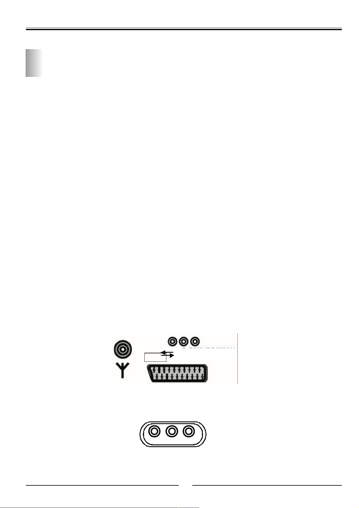
1.2 Connections
A/LA
EURO AV
PCM
Rear Connections
VIDEO L AUDIO R
Side Connection
5
Page 6
PT 90 NEAT Service Manual
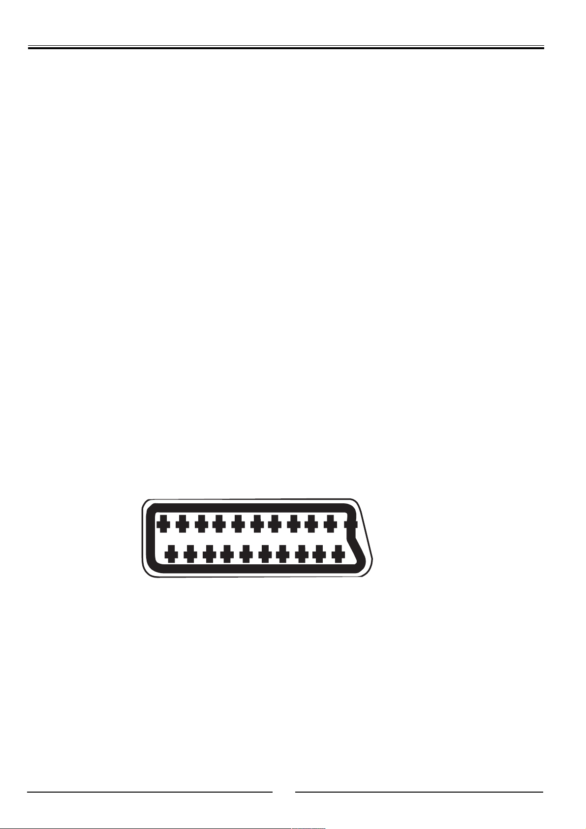
EURO SCART
I- Audio output 1. right channel 0.5 VRMS/<l k 0
2- Audio input 1. right channel 0.5 VRMS (connected to No.6)
3- Audio output 2. left channel 0.5 VRMS (connected to No.1)
4- GND (audio)
5- GND
6- Audio input 2. left channel 0.5 VRMS/>10k 0
7- RGB input, blue (B)
8- Switch signal video (status)
9- GND
10- Reserved for clock signals (not connected)
11- RGB input, green (G)
12- Reserved for remote control (not connected)
13- GND
14- GND switch signal RGB
15- RGB input, red (R)
16- Switch signal RGB
17- GND (video)
18- GND19- Video output 1 Vpp/75 ohm
20- Video input 1 Vpp/75 ohm
21- Shield
13579111315171921
2 4 6 8 10 12 14 16 18 20
6
Page 7
PT 90 NEAT Service Manual
14 NEAT CTV 001
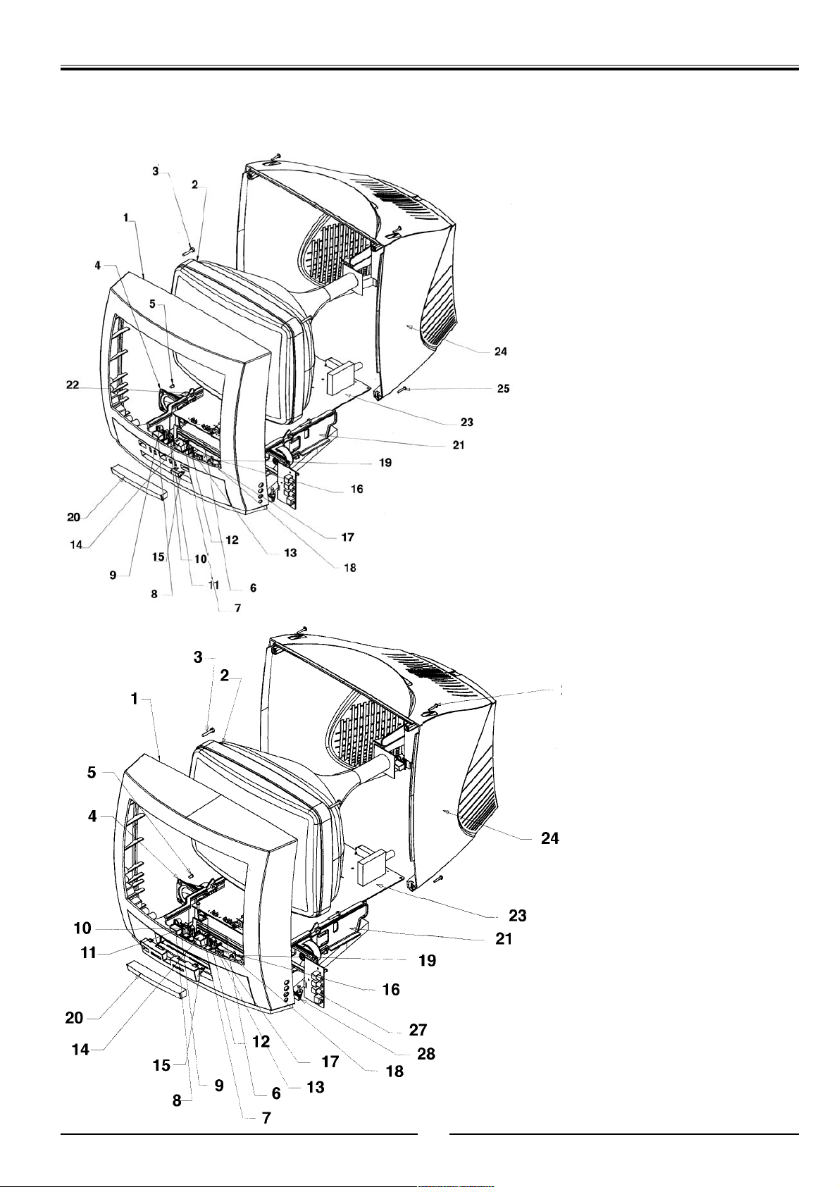
CHASSIS OVERVIEW
1- FRONT CABINET 002
2- PICTURE TUBE
3- PICTURE TUBE SCREW
4- SPEAKER
5- SPEAKER SCREW
6- DVD DRIVER
7- DVD DRIVER SCREW
8- EJECT BUTTON 001
9- EJECT BUTTON 001 SCREW
10- MULTIBUTON LEFT
11- MULTIBUTON LEFT SCREW
12- MULTIBUTON RIGHT
13- MULTIBUTON RIGHT SCREW
14- ON-OFF BUTON
15- ACYRILIC WINDOW 001
16- INFRA LED PCB
17- INFRA LED PCB SCREW
18- REFLECTOR
19- REFLECTOR SCREW
20- DVD HEAD
21- CHASSIS RAIL RIGHT
22- CHASSIS RAIL LEFT
23- MAIN CHASSIS
24- BACKCOVER
25- BACKCOVER SCREW
26- STYROPHOR
14 NEAT CTV 002
1- FRONT CABINET 002
2- PICTURE TUBE
3- PICTURE TUBE SCREW
4- SPEAKER
5- SPEAKER SCREW
6- DVD DRIVER
7- DVD DRIVER SCREW
8- EJECT BUTTON
9- EJECT BUTTON SCREW
10- MULTIBUTON LEFT
11- MULTIBUTON LEFT SCREW
12- MULTIBUTON RIGHT
13- MULTIBUTON RIGHT SCREW
14- ON-OFF BUTON
15- ACYRILIC WINDOW 002
16- INFRA LED PCB
17- INFRA LED PCB SCREW
18- REFLECTOR
19- REFLECTOR SCREW
20- DVD HEAD
21- CHASSIS RAIL RIGHT
22- CHASSIS RAIL LEFT
23- MAIN CHASSIS
24- BACKCOVER
25- BACKCOVER SCREW
26- STYROPHOR
27- AVPCB
28- AVPCB HOLDER
7
Page 8

PT 90 NEAT Service Manual
KEYBOARD
All the keys on the keyboard are used same as the relevant keys on the RC. But navigation in menus is quite different. In order to open Main Menu from keyboard V+ and V- keys must be pressed together. After displaying the
menus P+ and P- keys will be used as Navigation Up and Navigation Down keys. There is no enter key on the keyboard so V+ or V- will be used as Menu Right key if a submenu item is highlighted on the menu. These two keys will
also be used as Navigation Left and Navigation Right keys in order to change any highlighted options right side
value. To return previous menu V+ and V- keys should be pressed together.
2. SAFETY INSTRUCTIONS AND WARNINGS
SAFETY INSTRUCTIONS FOR SERVICE
REPAIRS
1. Use only the original spare parts with the same specifications for replacement.
2. Only the original fuse value should be used.
3. Safety components, indicated by the symbol, should
be replaced by components identical to the original ones.
4. Main leads and connecting leads should be checked for
external damage before connection. Insulation must be
checked.
5. Parts contributing to the safety of the product must not
be damaged or obviously unsuitable. This is valid especially for insulators and insulating parts.
6. Thermally loaded solder pads are to be sucked off and
re-soldered.
7. Ensure that the ventilation slots are not obstructed.
8. Potentials as high as 25 KV are present when this
receiver is operating. Operation of the receiver outside the
cabinet or with back cover removed involve a shock hazard
from the receiver.
9. Servicing should not be attempted by anyone who is not
thoroughly familiar with precautions necessary when working on high voltage equipment. Perfectly discharge the
high potential of the picture tube before handling it. The
picture tube is highly evacuated and if broken. Glass fragments will be violently expelled. Always discharge the picture tube anode to the receiver chassis to keep of the
shock hazard before removing the anode cap.
10. Keep wire away from the high voltage or high temperature components.
11. When replacing a wattage resistor, keep the resistor
10mm away from the circuit board.
12. Fast heating up (e.g. by bringing the Combi from a cold
place into warm and humid room) can result in moisture
condensing on the pickup lens of the DVD Module, thus
influencing the playability for a certain time. Before checking the performance, the DVD Loader should be stabilized
for at least 4 hours.
13. Never try to repair DVD module when it is ON. The
laser beam is highly dangerous and it may cause permanent damages.
HANDLING THE MOS CHIP COMPONENTS
MOS circuit requires special attention with regard to static
charges. Static charges may occur with any highly insulated plastics and can be transferred to persons wearing
clothes and shoes made of synthetic materials. Protective
circuits on the inputs and outputs of MOS circuits give protection to a limited extend only due to time of reaction.
Please observe the following instructions to protect the
components against ESD.
1. Keep MOS components in conductive package until they
are used. Most components must never be stored in styropor materials or plastic magazines.
2. Personnel must not touch the MOS components to avoid
electrostatic discharging.
3. Hold the component by the body touching the terminals.
4. Use only grounded instruments for testing and processing purposes.
5. Remove or connect MOS Ics when operating voltage is
disconnected.
6. Personnel in charge must make sure that they are connected with the same potential as the mass of the set by a
wristband with resistance.
X-RAY RADIATION PRECAUTION
1. Excessive high voltage can produce potentially hazardous X-RAY radiation. To avoid such hazard, the high
voltage must not be above the specified limit. The nominal
value of the high voltage of this receiver is 25KV at zero
beam current (minimum brightness) under 220 V AC power
source. The high voltage must not under any circumstance,
exceed 30KV. It is recommended the reading of the high
voltage to be recorded as a part of the service record. It is
important to use an accurate and reliable high voltage
meter.
2. The primary source of X-RAY radiation in the TV receiver is the picture tube. For continued X-RAY radiation protection, the replacement tube must be exactly the same
type tube as specified in the part list.
8
Page 9
4
2
2
1
0
5
/
/
/
7
7
/
4
/
1
7
/
1
/
4
_
_
7
0
_
_
7
_
7
6
1
_
1
8
5525149
44237363534
2
/
6
/
_
8
2
113151617181925
2
3
140
4
1
1
2
3
1
2
2
0
7 6
6
2
2
2
2
2
1
2A7
N
1
V
_
_
2
4
51618
8
8
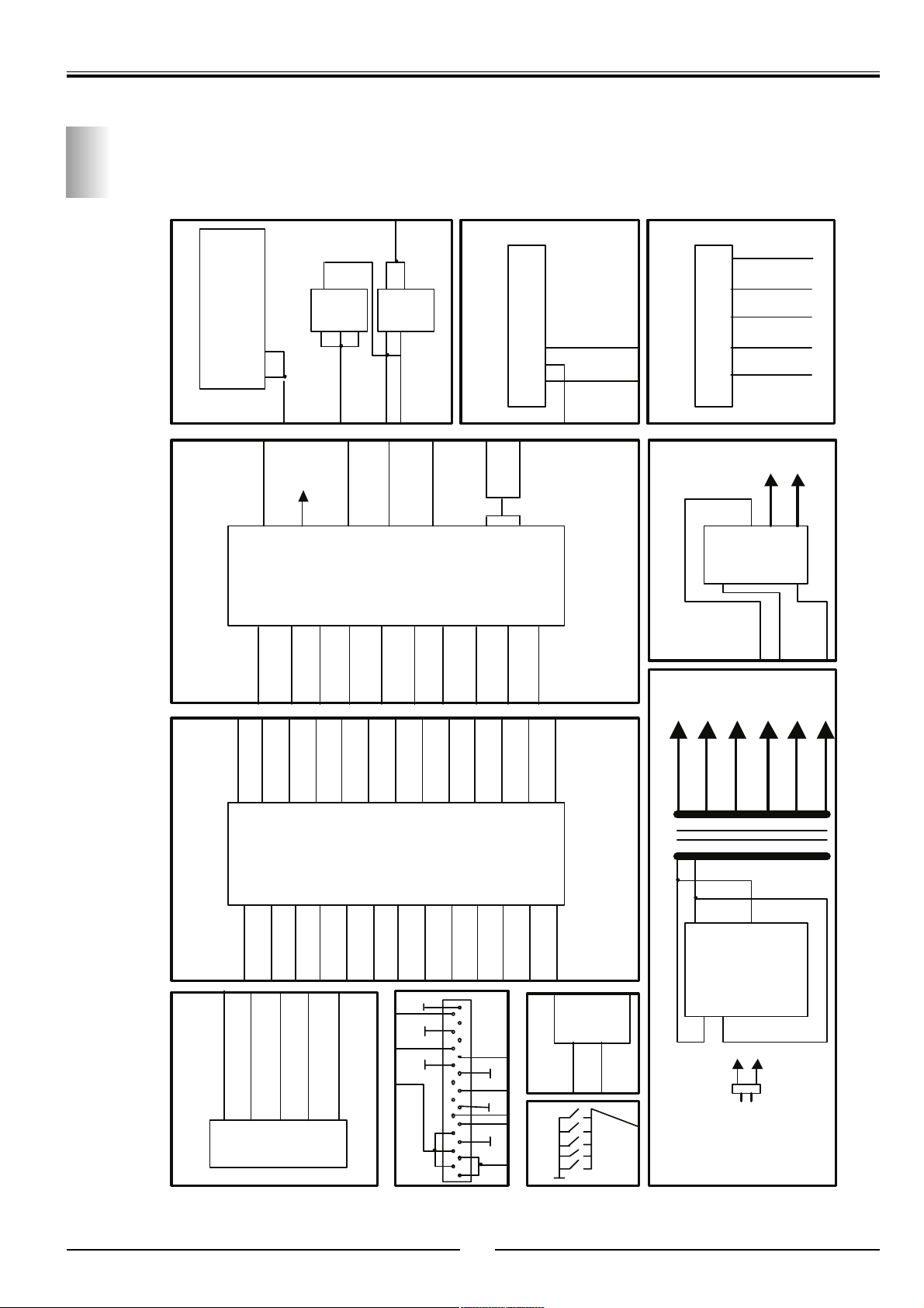
3. BLOCK DIAGRAM
3B
IA03
MN405
12
IA01
TDA7057
56
921
IC0
ST92195
8
18
1
KEYB
1
1
VOL
DVD SB
4
1
AUDOUT A
1
VOL
4
1
2
R_DVD
A10-3
MUTE_DVD
A8-10/A10-1/A7 -1
1
OSD A
V
4
I060
2
L DVD A1
4
LM358
1
A
7
HEATER A
3
ID41 TDA177
34
2
A9 VERTICAL
A2 -6
FB_OSD
CVBSOUT
333
A7-5/A2-10
1
VERT A2
PT 90 NEAT Service Manual
2
AMP A2
1V
A10 AV INTERFACE
OSD A7
V
SS08
CONN.
FBT
1
1
1
24 V12
8
4
1
3
BCL A2
3
9
2
HOUT A2
A
R DVD
2
A
L DVD
MUTE
1/A8-1
_DVD A7-
A8-4
DOUT
A8-5
CVBS_DVD
HEATER
A7 -CONTROLLER A8 AUDIO AMPLIFIER
A2 VIDEO PEOCESSOR
1
MUTE_DVD
A8-10/A8-1/A10-1
CLI 1L/L
2
3
A
A
2
1
A
A
2
1
AUDOUT A8
5
47
ICV1
STV2246
1
L/L
SDA A
2
5/A
IF1 A
SCL A
6
5/A
IF1 A
1/A
SD
1
TV/DVD A
7
2
A
1
HEATER A6
HOUT A
4847464
7
8
4
AGC
IF2
2/A
CL A
4
1
A1 TUNER
G OSD A2
B OSD A25R OSD A2
1
BCL A
VERT
111413202526272
2
1
IN
SC
AV STATUS A3
3
CVBS A
5
FBEXT A
2
SC_I A
FB_OSD
A2-10/A7-5
6
CVBSOUT A7
3
CVBS A
A3 SCART
1
OSD A
AMP A
FB
V
4
8
CV BSEXT A3
B
9
20
SCART1
19
14
5
1
15
18
21
10
11
12
17
8
7
6
13
4
3
2
SS01
SDA
A2-1/A4-1/A1-1
OSD A
R
7
G
7 R A2-6
1 G A
8 CLI A
B A
A2 -1
AV_STATUS
SCL
A2-2/A4-2/A1-2
OSD A
G
R 6FBEXT A
A11
OSD A
B
5
IC0
A4
KEYBOARD
SDA
110
16
5
12V
8
5
WP0
1
IP01
TDA16846
3142
24C08
5
6
A
SCL
A
A7-1/A2-1/A1-1
1
A5 POWER SUPPLY A6 HORIZONTAL
KEYB A7
AC I
9
Page 10
PT 90 NEAT Service Manual
T
V
16
V
D002
D001
D0045VD005
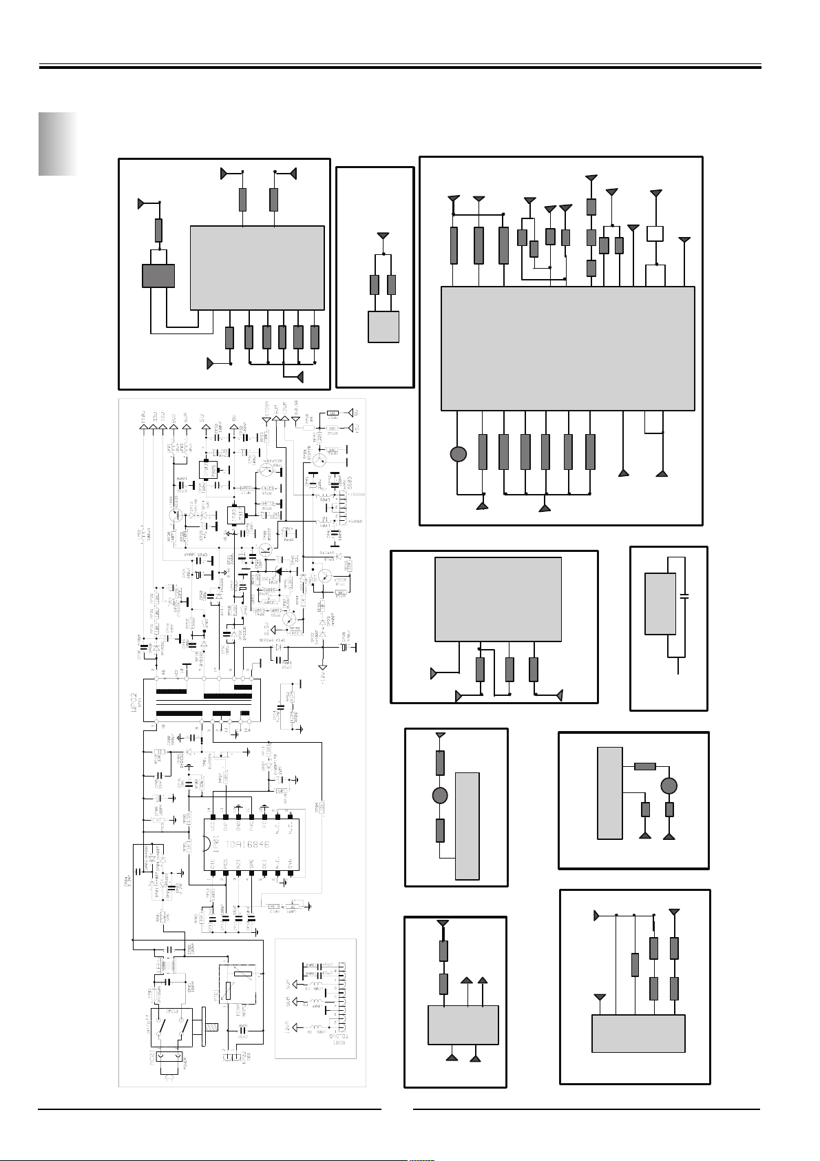
4. SUPPLY VOLTAGE DIAGRAM
5VDVD
12VDVD
R081
45
19
R012
R052 R028 RA09
20
R013
5V
5V
5VA
5VA
5VA
T001
43
393433
40
41
21
5VD
31
25
26
5VA
5V
VIDEO
1
5V
LV01
PROC.
STV2246/47/48
2
12
LV01
53
LV03
17
DV23
8V
LV07
SA02
A2
A5 POWER SUPPLY
LV01
45
252627
DV22
DV21
8V
DV20
28
8V
+12V TO RA10
A8
RA11
IA03
8V
11
MN4
053
RS58
5V
R002
R008
56
ST92195/92185
2
T003
A7
5V
55
R011
5V
R080
R057
54
3
12
R010
13
R007
46
14
R032
5V
A1
TV01
33V
RV03
RV06
RD15 RD12
FB
TUNER
9
5V
8V
19
8V
24V12
4
8
1
7
LT01
SS05
3
2
3
RT03
8V TO SS05/4
1
RT01
5V
A10
1 8
C011
EEPROM
5V
A4
RV54
14
5V
TV05
RV57
8V
12
DV10
SS08
12V
8
RD45
24V
9
8
TDA1
RD44 RD56
RD28 RD40
7
4
1
771
A6 A3
110V
16V
A9
10
Page 11
TRT
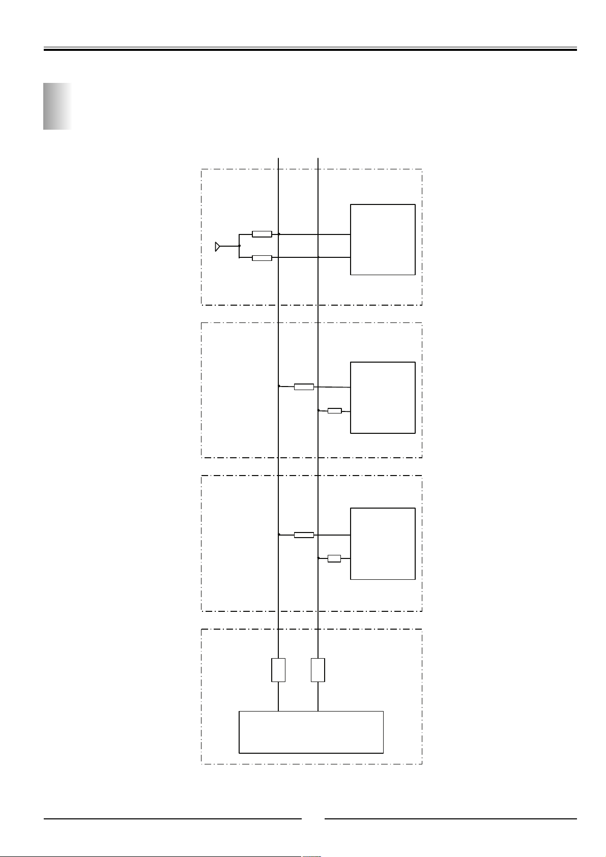
5. I2 BUS INTERCONNECTION DIAGRAM
PT 90 NEAT Service Manual
+5V
A7
A4
R012
R013
SDA
SDA
SDA
SCL
R049
SCL
SCL
R048
20 19
6 5
u-CONTROLLER
EEPROM
A2
A1
SDA
SDA
TUNER
RV34
SCL
R
SCL
5
4
RV33
52
51
PROC.
VIDEO
11
Page 12
PT 90 NEAT Service Manual
Fuse
F1 defective
Voltage at drain
TP 01
Voltage at
IP01
PIN 11
< 1V
Start-up voltage
(6)
PIN 14
< 8V
Start-up voltage
varies ca. 8V
IP 01
Measure
+115V
adjustable with
VAP 01
Control range of
switched-mode
power supply
DP01 - 04
CP01 - 04
CP06, TP01
RP 07, RP 05
open and
short circuit
RP 06
RP 11, DP 07
TP 01
VAP 1, RP 03
YES
NO
YES
YES
NO
NO
NO
Switched mode power
supply defective, +110V
is missing or level is wrong
NO
YES
YES
YES
NO
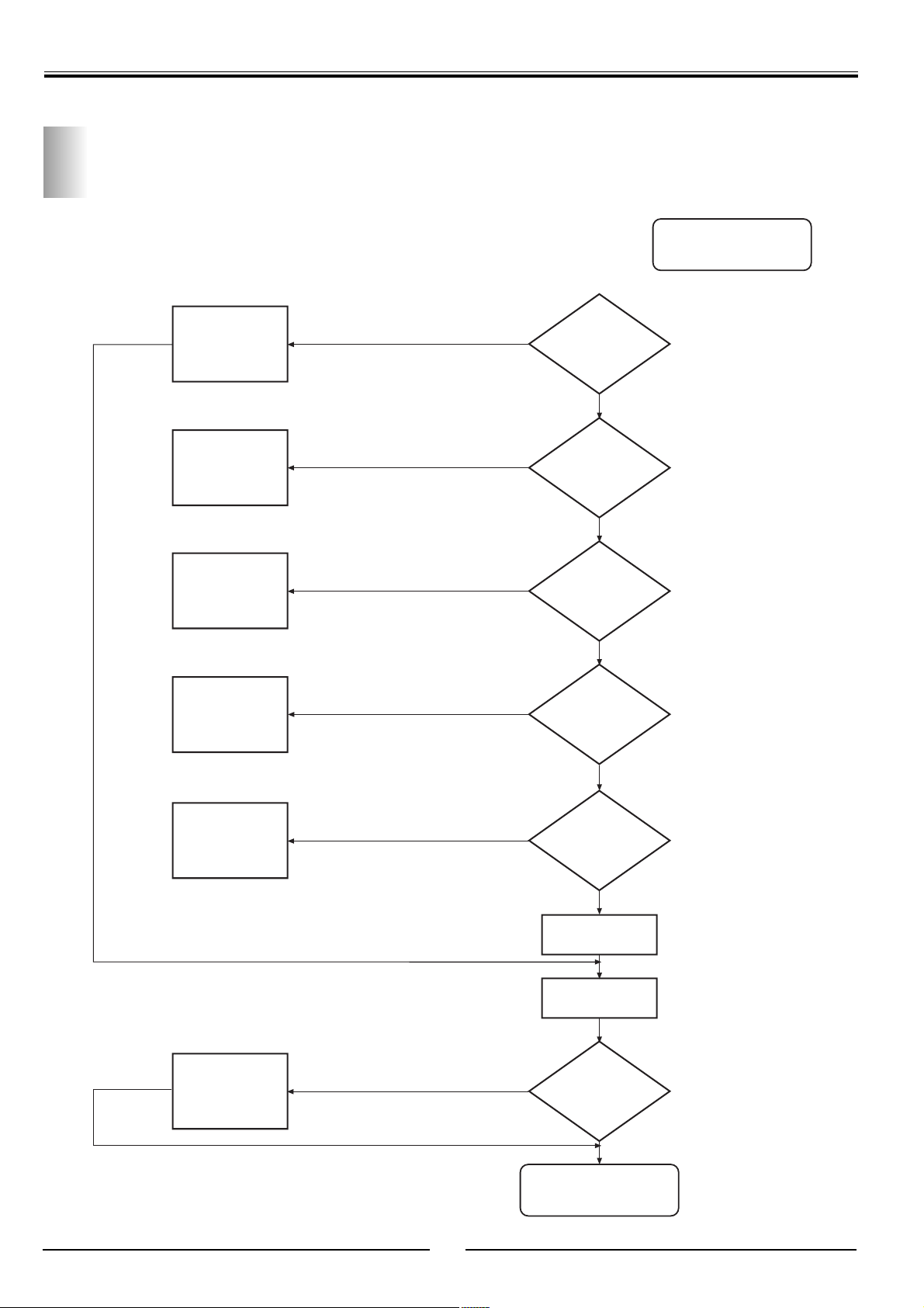
6. FAULT TRACING DIAGRAM-POWER SUPPLY
12
Page 13
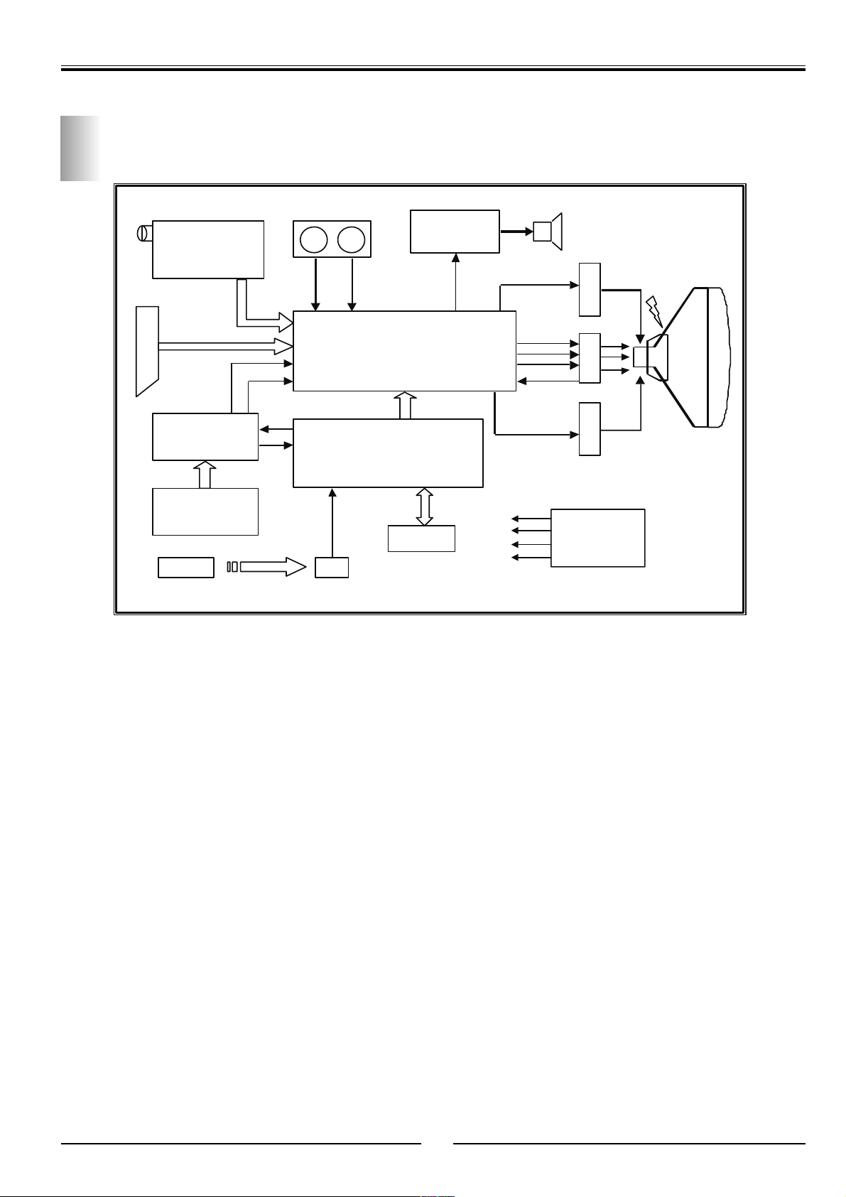
7. CHASSIS DIAGRAM
FRONT AV
PLL TUNER
TDA 7057
PT 90 NEAT Service Manual
2 X 2W
H.YOKE
BU508D
SCART
CVBS
AUDIO
DVD
BOARD
DVD
LOADER
RC IR
STV224X
ST92195
24C08
+5V
+110V
+12V
+16V
R G B
TDA1771
POWER
V.YOKE
13
Page 14

PT 90 NEAT Service Manual
8. SERVICE MENU AND BASIC ADJUSTMENTS
SERVICE MODE IS ACTIVED BY PRESSING THE DIGIT 1923
AT FEATURES MENU
8.1 OPTION BYTES
OPTION 1: MODEL CONFIGURATION
b0: 1: L Avaialable 0: not available
b1: 1: APR ON 0: APR OFF
b2: 1: no Pin 8 16:9 switching mode 0: Pin 8 16:9 switching mode
b3: 1: Turn on with AV button 0: not used
b4: 1: Keyboard with menu 0: Keyboard without menu
b5: 1: Brightness half range available 0: Brightness full range available
b6:7 Main Tuner
00 : Samsung
01 : Temic
10 : Philips UV1316
11 : Thomson/Orega
OPTION 2: FEATURE CONFIGURATION
b0: 1: AV2 mode available 0: not available
b1: 1: SVHS mode available 0: not available
b2: 1: Volume linear 0: Volume Logaritmic
b3 1: Search mono audio ident available 0: not available
b4: 1: DVD picture in SVHS mode 0: DVD picture in RGB mode
b5: 1: Headphone available 0: not available
b6: 1: No Subwoofer 0: Subwoofer available
b7: 1: 4/3 Picture tube 0: 16/9 Picture tube
OPTION 3: VIDEO/AUDIO FEATURE CONFIGURATION
b0: 1: One Crystal application (4.43 Mhz) 0:Two cystal application (for NTSC playback)
b1: 1: Intercarrier application 0: QSS application
b2: 1: STV2248E 0: Normal video IC
b3: 1: OSD contrast control ON 0: OSD contrast control OFF
b4: 1: Blue screen enable 0: disable
b5: 1: AVC Automatic Volume Correction (MSP Stereo) AVL(Mono 22XX)
0: not available
b6: 1: DVD available 0: not available
b7: 1: Standby after power on 0: No Standby after power on
Reserved bits must be set to 0
You will need following equipments to carry out the adjustment procedures;
a- PLL Pattern generator for Secam L'
b- PLL Pattern generator PAL BG
c- Patern generator for white pattern
d- Color Analyzer (CA100)
14
Page 15

PT 90 NEAT Service Manual
8.2 GEOMETRY ADJUSTMENT
a. V.S 4/3 50H
b. V.S 16/9 50H
c. V.S 4/3 60H
d. V.S 16/9 60H
e. V.P
f. H.P
• Enter service menu and select the GEOMETRY settings
• Standart geometrical adjustments carried out by V.S, V.P and H.P settings. V.S 16/9 50h setting have to be carried
out until 3 cm distance between upper and lower parts of the screen.
• Same adjustments for 60H for 16/9 and 4/3.
• Press menu button to leave service menu
Menu button to leave service menu.
8.3 G2 ADJUST
> : <
increase normal decrease
Enter the G2 menu in the service mode
Turn the G2 potentiometer on FBT until you reach the : sign
< indicator means to decrease
> indicator means to increase
8.4 VIDEO
1 RED
2 GREEN
3 BLUE
4 RED COFF
5 GREEN COFF
• Apply Dark gray pattern (at 10 IRE)
• Contrast 70%, brightness middle, color saturation middle.
• By changing the R COF and G COF Adjust to obtain the necessary values for x and y.
• Apply white pattern (at 100 IRE)
• Set the contrast to 70%, brightness and color saturation to middle.
• Place the color analyzer.
• (R,G,B), it is possible to modify the peak white.
• Adjust to obtain the necessary values for x and y.
Remark: It may be necessary after low light alignment to check and to re-align the high light and to repeat several
times the procedure to obtain good alignment for both low and high light.
15
Page 16

PT 90 NEAT Service Manual
8.5 TUNER/ IF
1. AGC
2. P C
3. P F
4. P C.L’
5. P F.L’
PPIIFF aaddjjuussttmmeenntt ffoorr BBGG//DDKK//LL ssyysstteemmss::
• 38.9 MHz PAL BG signal applied Tuner via tuner output (IF output).
• Leave the channel settings menu and enter service menu. Enter TUNER IF menu in the service mode.
Choose the PIF COARSE and PIF FINE item and adjust the setting until the : indicator (displayed as > : <)
turns in red color by pressing < and > on remote control.
• Press Menu button to leave service menu.
PPIIFF aaddjjuussttmmeenntt ffoorr LL'' ssyysstteemm::
• 33.9 MHz SECAM L' signal applied Tuner via tuner output.
• Leave the channel settings menu and enter service menu. Enter TUNE IF menu in the service mode.
Choose the PIF COARSE L’ and PIF FINE L’ item and adjust the setting until the: indicator
(displayed as > : < ) turns in red color by pressing < and > on remote control.
• Press Menu button to leave service menu.
8.6 HOTEL MODE
Installation and Child Lock Menus are omitted in Hotel Mode. You can not search any channel when the
Hotel Mode is activated.
Volume level cannot be increased higher then certain level in Hotel Mode. The volume limiting level is a predefined value in service menu.
Hotel mode activated from service menu.
8.7 SYSTEM VOLTAGE ADJUSTMENT
• Switch the TV in AV mode by pressing AV button on remote control unit. (Minimum beam current condition)
• Adjust the VAP2 potentiometer until 110Vdc measured on cathode pin of DP08 diode.
16
Page 17
PT 90 NEAT Service Manual
9. DVD MODULE
9.1 SAFETY AND HANDLING PRECAUTIONS
1. DO NOT use and store the Loader in dusty, high temperature or high humidity environments.
2. To avoid damage to the Loader by electrostatic dischargers, measuring equipment and operators should be
grounded during handling. The user of this unit takes all necessary precautions to avoid ESD (Electro-Static
Discharge) failures during handling and assembly of this unit into the end product.
3. Contamination of the PCB might influence the performance. Avoid fingerprints and stains on the PCB and
handle the Loader in a clean environment.
4. The mechanism of the Loader has been adjusted carefully during manufacturing. High shocks on this unit
may damage and should be avoided.
5. Fast heating (e.g. by bringing the Loader unit from a cold place into a warm and humid room) can result in
moisture condensing on the pickup lens, thus influencing the playability for a certain time. Before checking
the performance the Loader unit should be stabilized for at least 4 hours.
6. DO NOT disamble the loader to avoid ESD failures and to prevent from contamination.
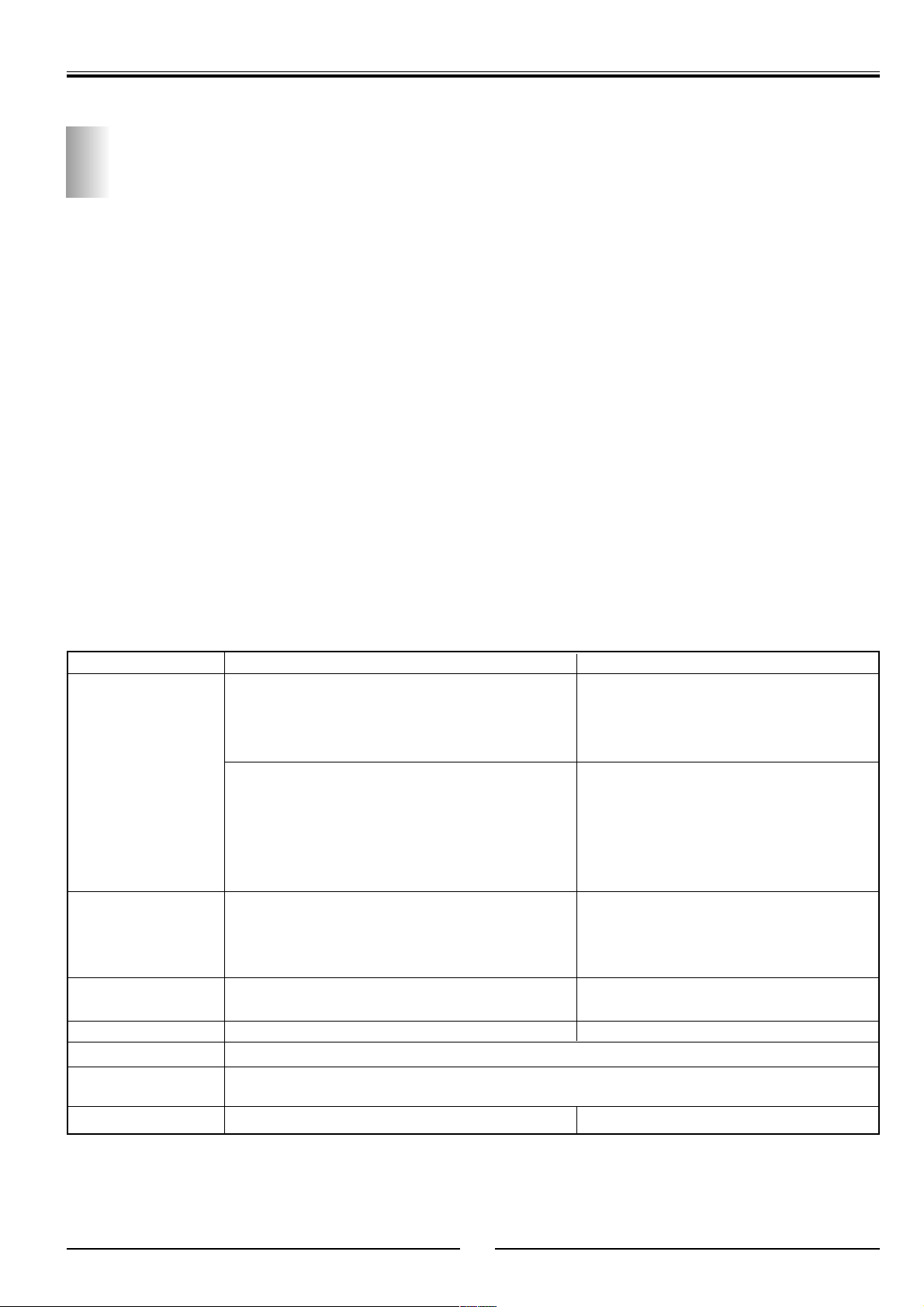
AACC SSoouurrccee SSuuppppllyy::
The Voltage Fluctuation : 110/220 V ± 10% tolerance
The Impulse Noise : 110/220 V ± 10% tolerance
AApppplliiccaabbllee DDiissccss FFoorrmmaatt
DDiisscc TTyyppee DDeessccrriippttiioonn
DVD-5 (Single Layer)
DVD-9 (Double Layer) IS09660
DVD-10 (Single Layer Double Side) UDE
DVD-18 (Double Layer Double Side) DVD BOOK
Disc Format
IS09660
RED BOOK (CD-DA)
WHITE BOOK (Video-CD)
CD BLUE BOOK (CD Extra)
YELLOW BOOK (CD-ROM)
ORANGE BOOK (CD-RW, R)
DVD-5 4.70 GB
DDiisscc CCaappaacciittyy
Disc Diameter DVD/CD 12 cm/8 cm
Disc Thickness 1.2 mm
Disc center
Aperture 15 mm
Track Gap 1.6 µm, CD 0.74 µm, DVD
DVD-9 8.54 GB
DVD-10 9.40 GB
DVD-18 17.0 GB
CD 656 MB (Mode 1)
748 MB (Mode 2)
17
Page 18
PT 90 NEAT Service Manual
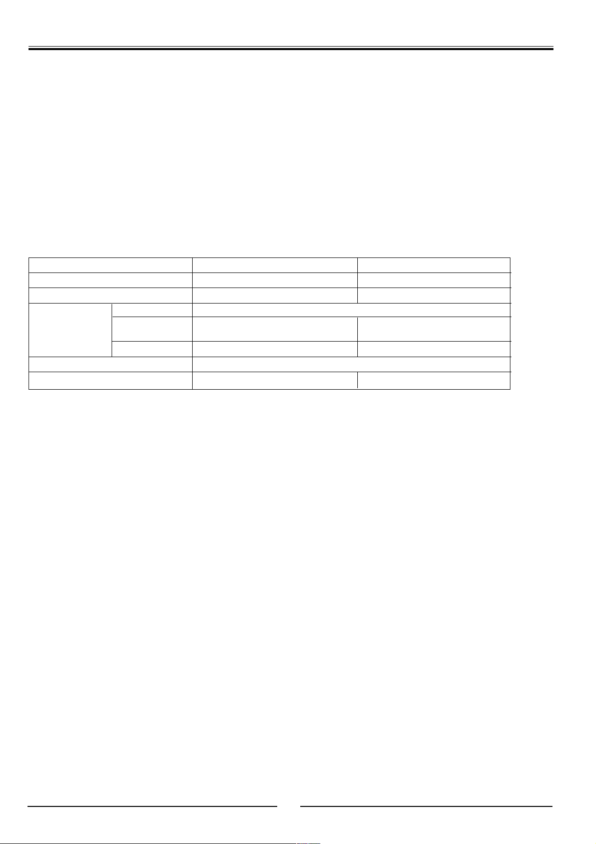
FFuunnccttiioonnss
Data Transfer Rate:
DVD 2600kB/sec (max)
CD 870kB/sec (max)
Data Buffer Capacity
256KB (DVD/CD)
Error Rate
10e
-15
MAX (DVD), 10e
-12
MAX (CD)
Reading Time
Starting procedure (Less than 15seconds)
Stopping procedure (Less than 2 Seconds)
LLaasseerr SSppeecciiffiiccaattiioonnss
DDVVDD CCDD
Laser wavelength 650-665nm 790+20nm
Laser power 0.5mW 0.7mW
Object Lens Non-spherical lens
lens Length of Ray
Coil 0.6mm 0.47mm
Moving Range 1.71mm 1.35mm
Focus Astigmatism
Searching Phase difference detection Three spot tracking
Disc Loading Mode
Motor- driven front-loading tray
Disc Fixing
Beam magnetic fixation
Reliability
Mean Time Between Failure (MTBF): Not less than 2,000 hours
Mean Time To Repair (MTTR): 0.5 hours
WWoorrkkiinngg EEnnvviirroonnmmeenntt
Temperature and Humidity
Operating temperature 5 – to 45 –
Storage temperature - 20 – to 60 –
Operating temperature varying 11–/hour(max)
Storage temperature varying 20–/hour(max)
Operating humidity 10% to 70%
Storage humidity 5% to 80%
Vibration
Reading data state 0.2g 10-30Hz sine wave
Playing CD audio state 0.15g 10-30Hz random
Standby 2.4g 10-30Hz random
Striking
Standby state 100kg 6ms half sine-wave (in X,Y and Z directions)
Noise
Not more than 45dB in one meter away
18
Page 19
9.2 MECHANICAL AND ELECTRICAL
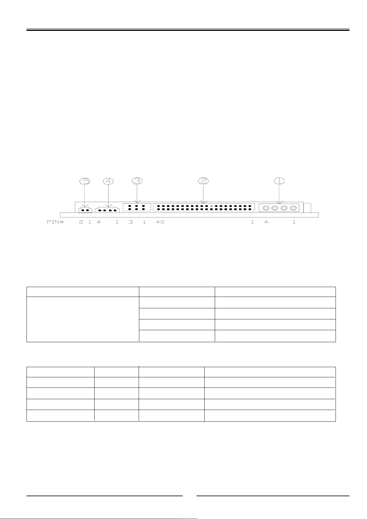
1. CONNECTORS
Integrated Connectors
1. DC power jack
2. IDE interface
3. Master/slave mode jumper set (not applicable as the loader configured for player)
4. Analog audio output (not applicable as the loader configured for player)
5. Digital Audio output (not applicable as the loader configured for player)
PT 90 NEAT Service Manual
PPiinn DDeeffiinniittiioonnss
ITEM PIN NO. DESCRIPTION
DC Power Jack 3 GND
SSiiggnnaall PPiinn NNoo.. PPiinn TTyyppee DDeessccrriippttiioonn
CSIEX- 37 I Driver Chip Select 0
CS3EX- 38 I Driver Chip Select 1
DA0 35 I Driver Address Bus-Bit 0
DA1 33 I Driver Address Bus-Bit 1
Power Jack
1 +12V
2 GND
4 +5V
ATAPI Interface
19
Page 20
PT 90 NEAT Service Manual
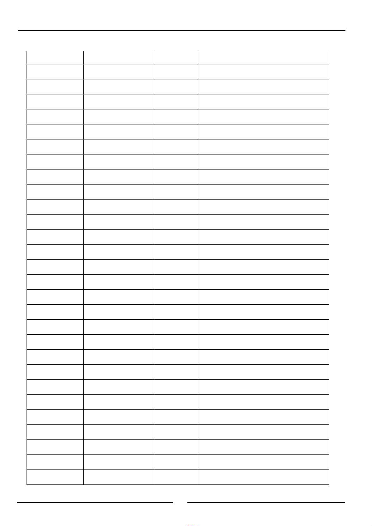
DA2 36 I Driver Address Bus-Bit 2
DASP- 39 I /O Driver Activity/Driver I Present
DD0 17 I /O Driver Data Bus-bit 0
DD1 15 I /O Driver Data Bus-bit 1
DD2 13 I /O Driver Data Bus-bit 2
DD3 11 I /O Driver Data Bus-bit 3
DD4 9 I /O Driver Data Bus-bit 4
DD5 7 I /O Driver Data Bus-bit 5
DD6 5 I /O Driver Data Bus-bit 6
DD7 3 I /O Driver Data Bus-bit 7
DD8 4 I /O Driver Data Bus-bit 8
DD9 6 I /O Driver Data Bus-bit 9
DD10 8 I /O Driver Data Bus-bit 10
DD11 10 I /O Driver Data Bus-bit 11
DD12 12 I /O Driver Data Bus-bit 12
DD13 14 I /O Driver Data Bus-bit 13
DD14 16 I /O Driver Data Bus-bit 14
DD15 18 I /O Driver Data Bus-bit 15
DIOR 25 I Driver I/O Read
DIOW- 23 I Driver I/O Write
DMACK- 29 I DMA Acknowledge
DMARQ- 21 O Driver Request
INTRQ 31 O Driver 16Bit I/O
IOCS16 32 O Driver Interrupt
IORDY 27 O I/O Channel Ready
PDIAG- 34 I/ O Passed Diagnostics
RESET- 1 I Driver Reset
CSEL 28 Cable Select
KEYPIN 20 Keying Pin on Interface Connector
20
Page 21
PT 90 NEAT Service Manual
2. KEY COMPONENTS
IItteemmss MMooddeell NNoo.. MMaakkeerr LLooccaattiioonn
Spindle Motor CCM03-042R1-2 MORETECH China
Loading Motor FC8A30T28_4A DM2429A SANKO TRICORE China Taiwan
Sled Motor FC8A30T18_2 DM2428 SANKO TRICORE China Taiwan
Laser Pick-up PVR-520T-HR-0101 MISTSUMI Japan
Actuator Drive BA5954FP Rohm Japan
Loading Motor Drive BA6287F Rohm Japan
RF Amp. SP3721A TI U.S.A
Servo DSP M5705 ALI Taiwan
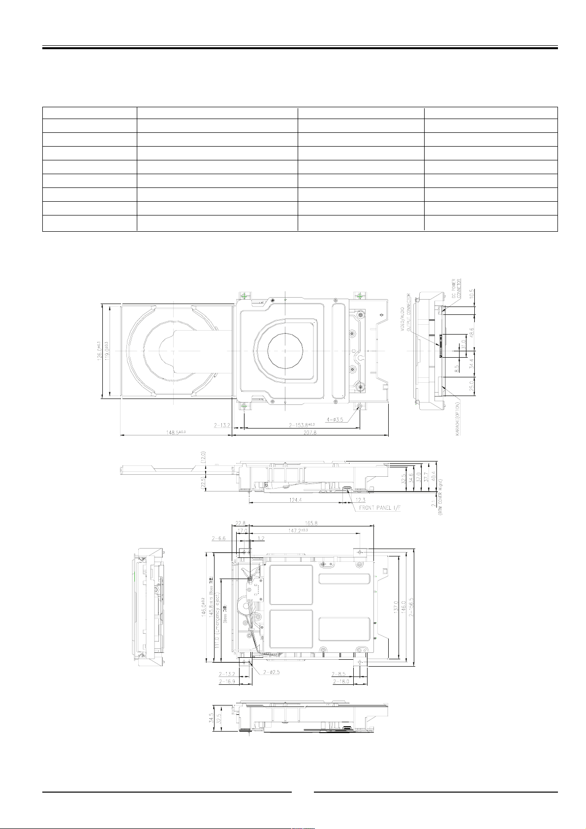
3. MECHANICAL DIMENSIONS
21
Page 22
PT 90 NEAT Service Manual
10- BLOCK DIAGRAMS
TV CHASSIS
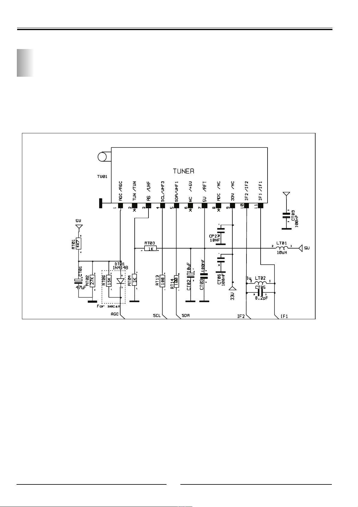
A 1 TUNER
22
Page 23
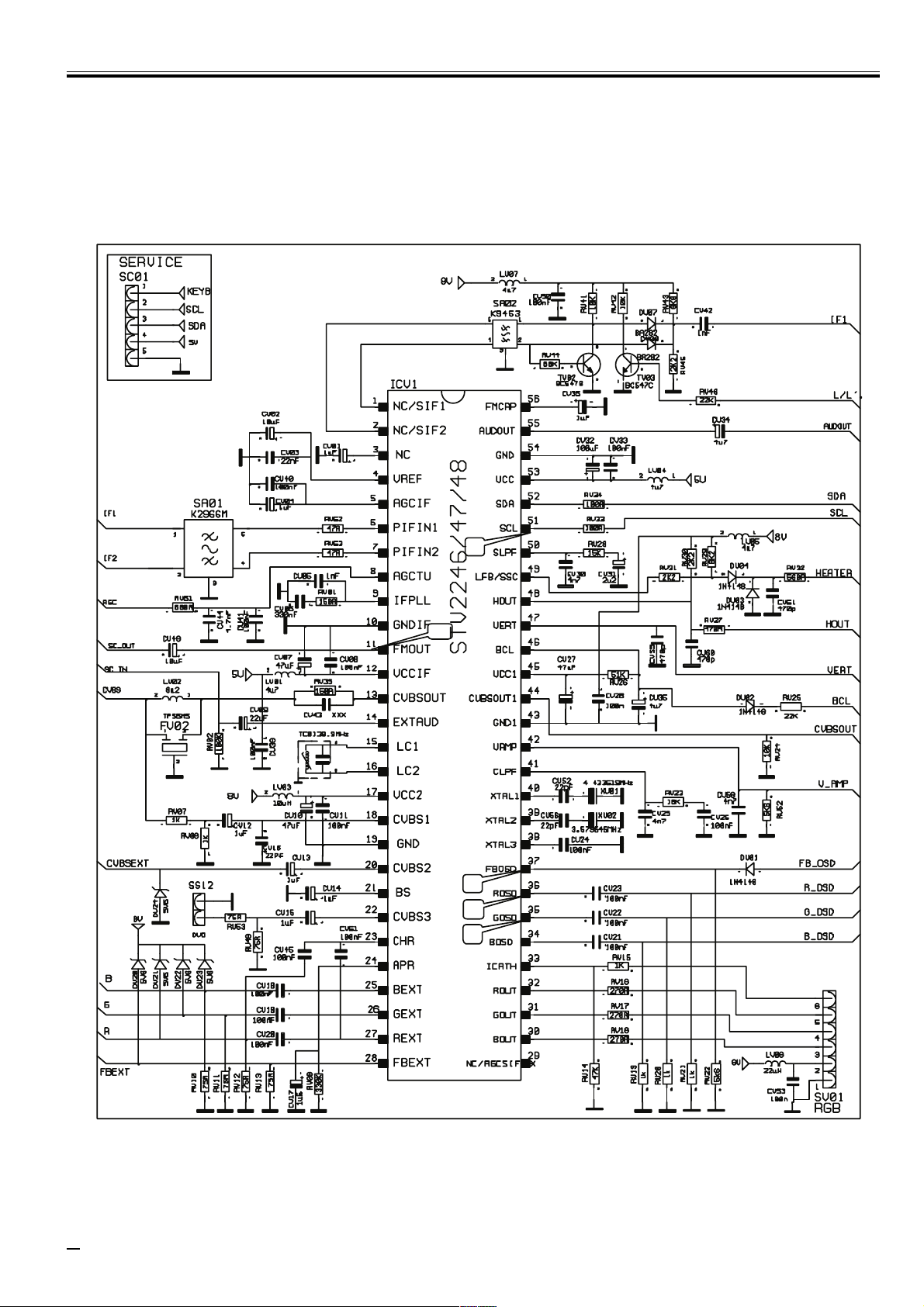
A 2 VIDEO PROCESSOR
PT 90 NEAT Service Manual
D1
D2
D5
D4
D
Page 24
PT 90 NEAT Service Manual
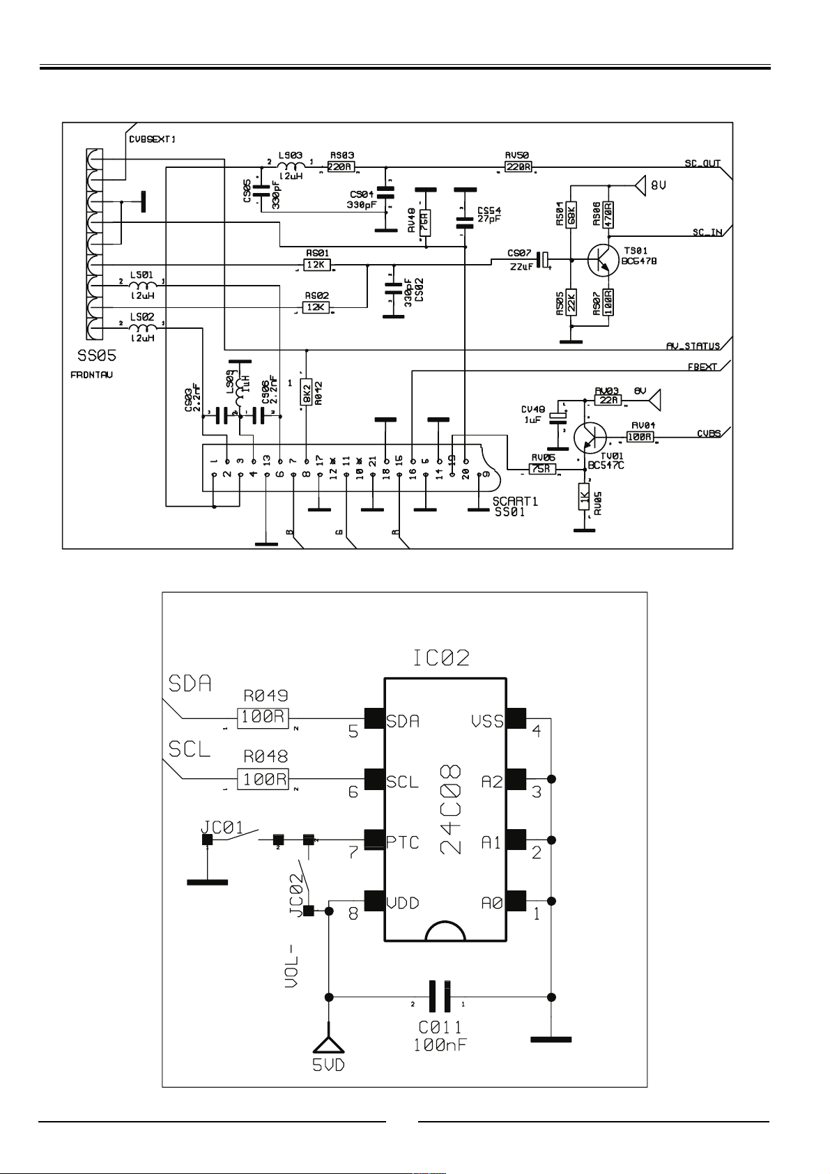
A 3 SCART
A 4 EEPROM
24
Page 25
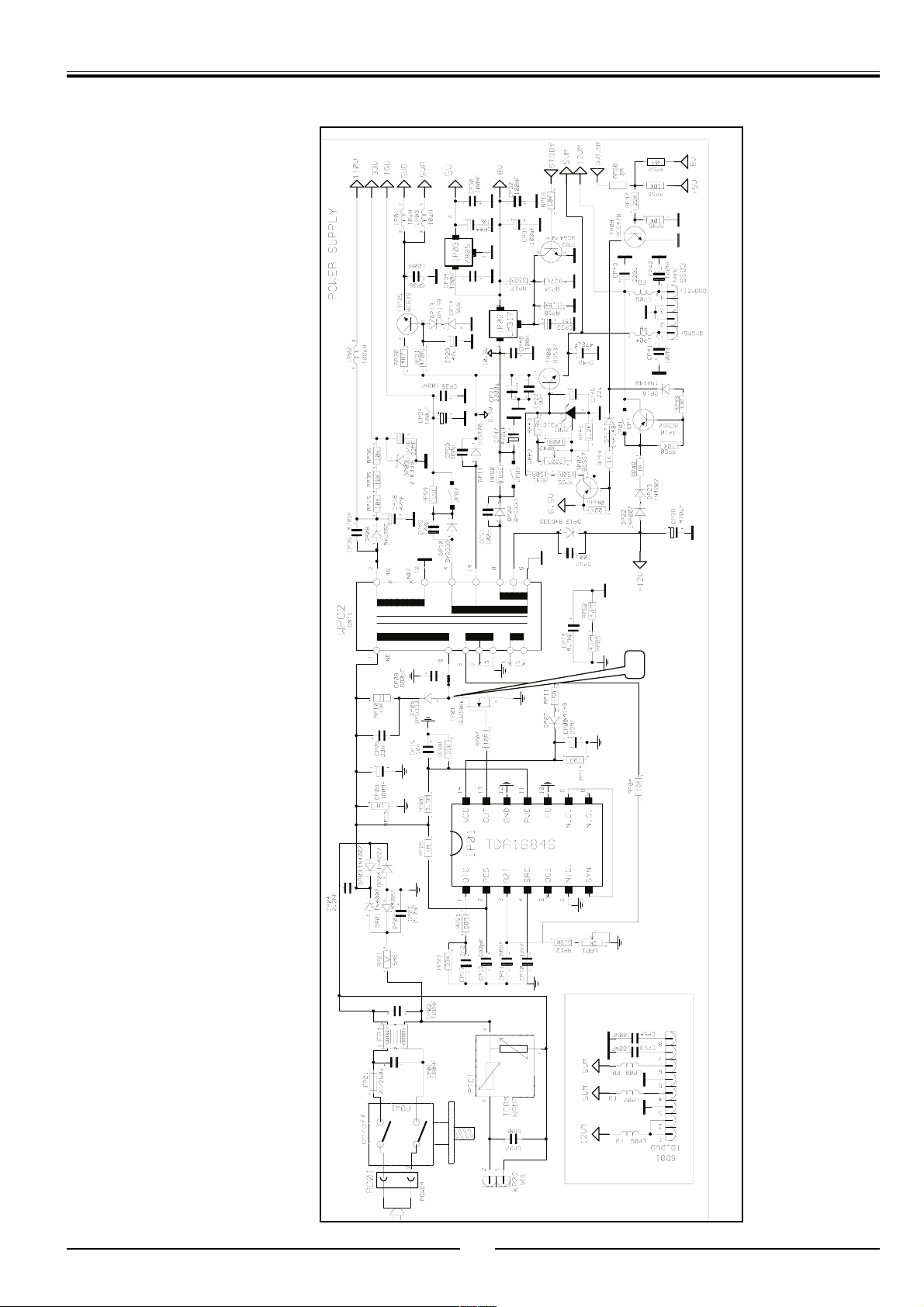
A 5 POWER SUPPLY
PT 90 NEAT Service Manual
E1
25
Page 26
PT 90 NEAT Service Manual
2
1
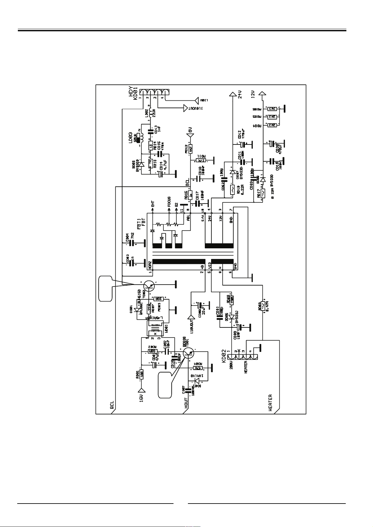
A 6 HORIZONTAL
F
F
26
Page 27
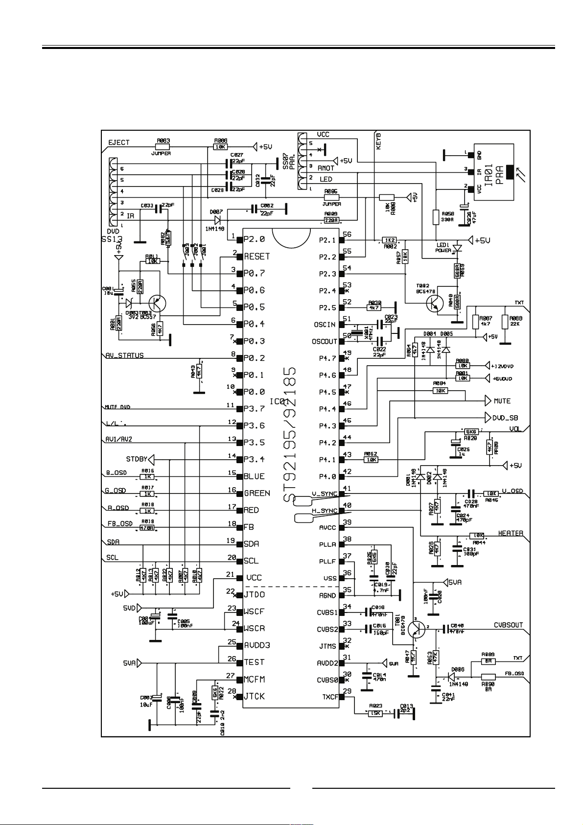
A 7 MICRO CONTROLLER
PT 90 NEAT Service Manual
G2
G1
27
Page 28
PT 90 NEAT Service Manual
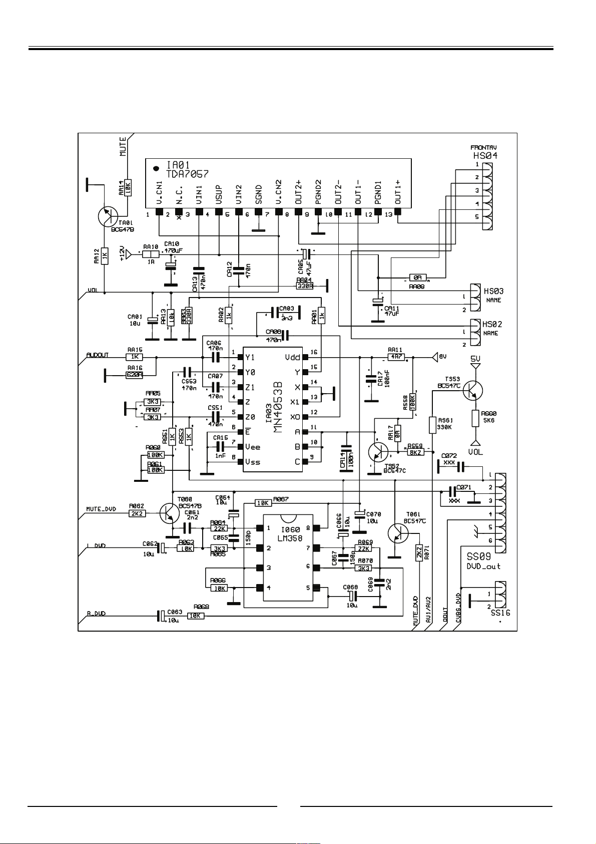
A 8 AUDIO AMPLIFIER
28
Page 29
H1
PT 90 NEAT Service Manual
H2
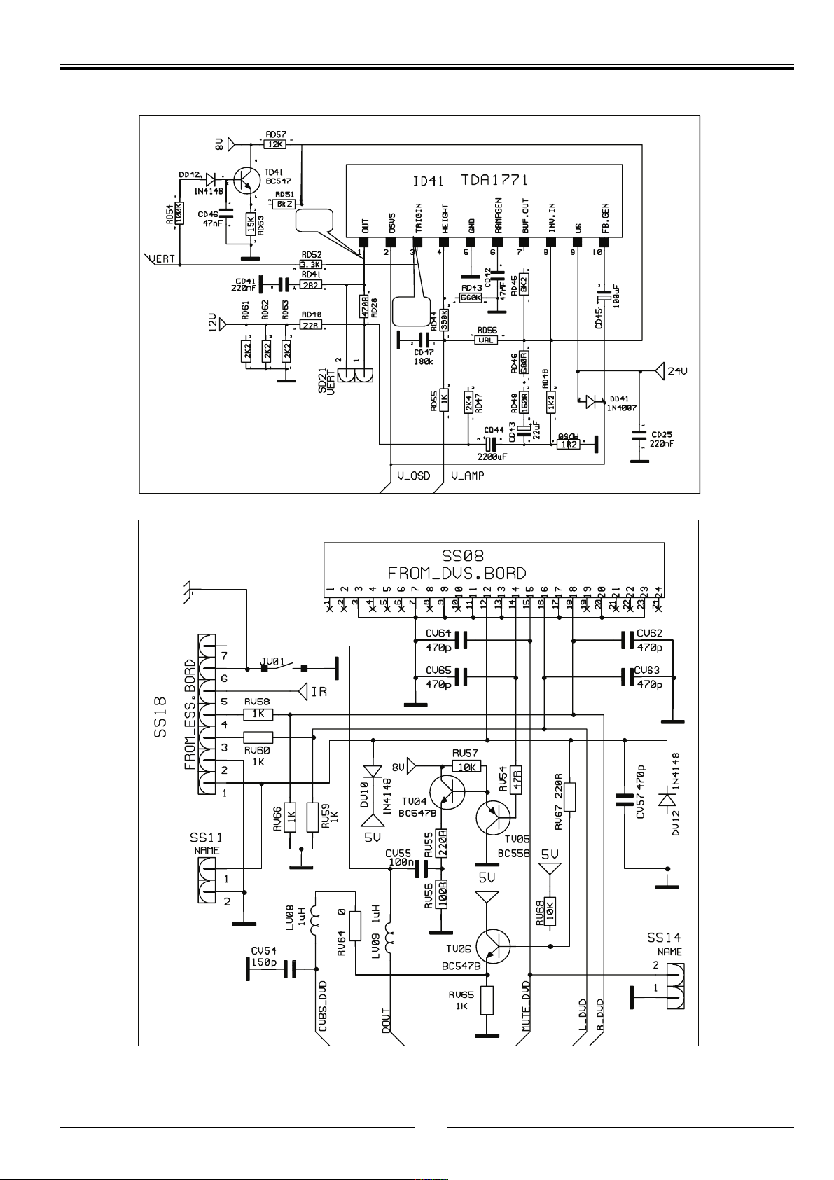
A 9 VERTICAL
A10 AV INTERFACE
CONNECTOR
29
Page 30
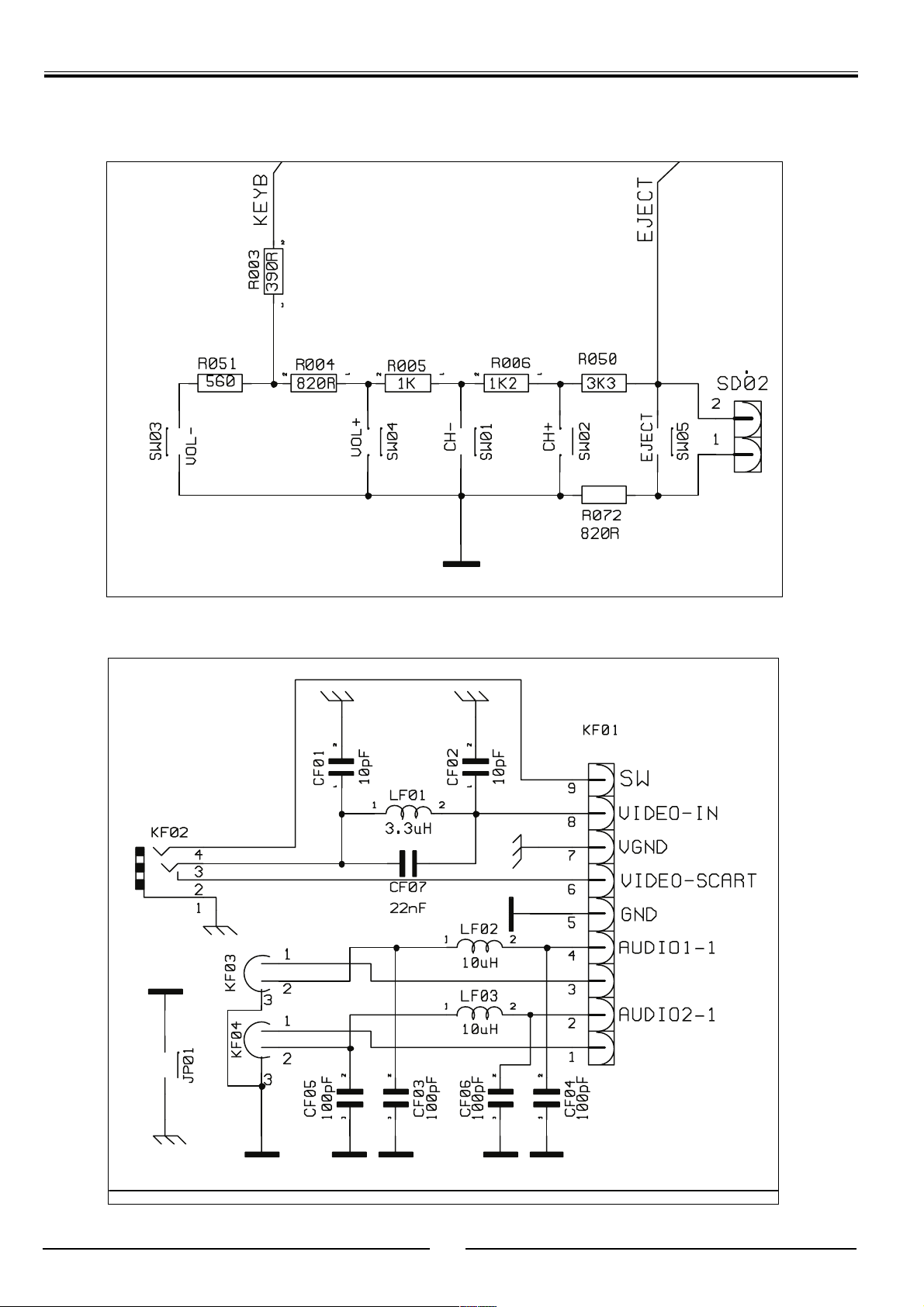
PT 90 NEAT Service Manual
A 11 KEYBOARD
A 12 FRONT AV
30
Page 31
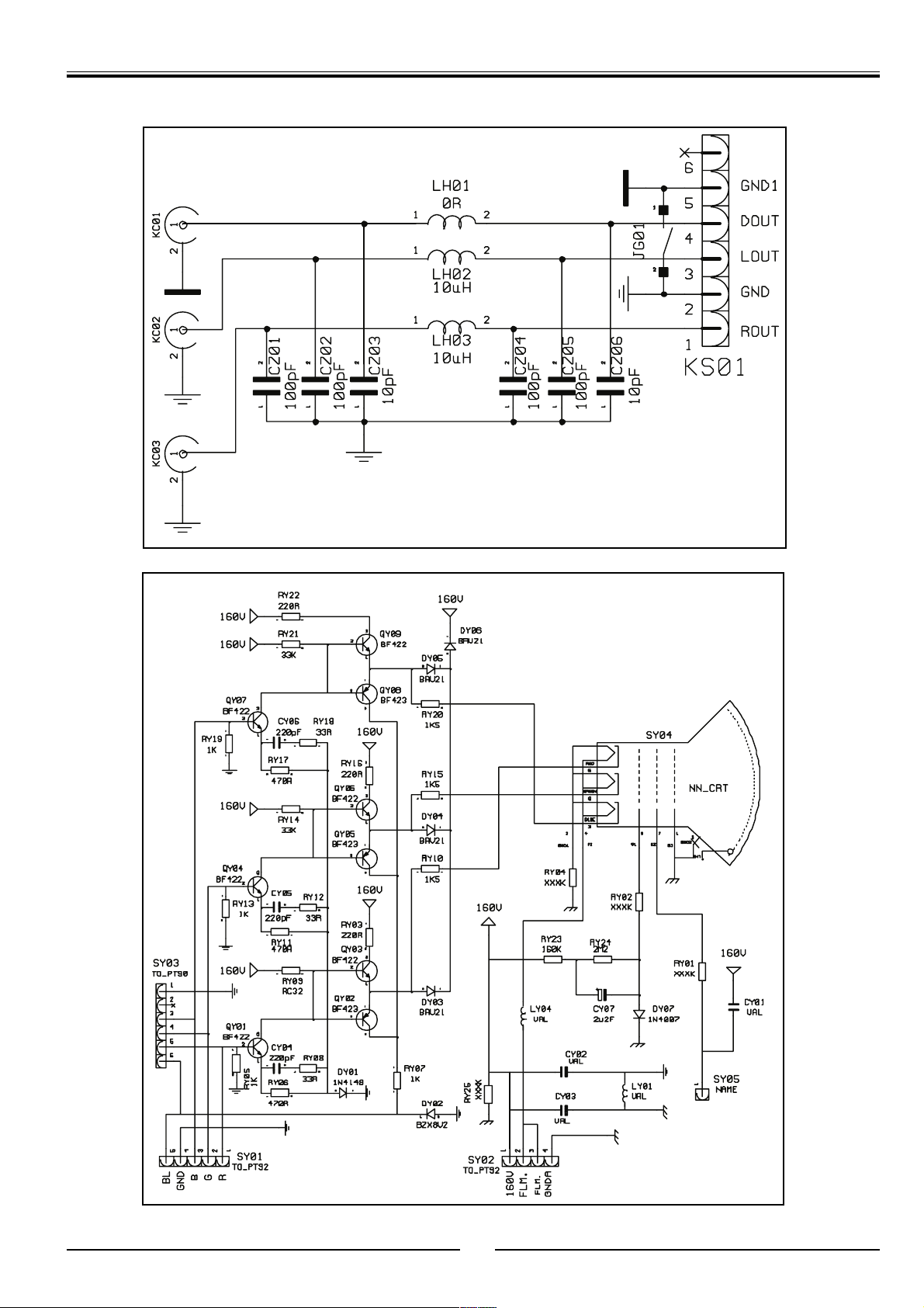
PT 90 NEAT Service Manual
A13 LINE OUT
A14 TUBE MODULE
31
Page 32
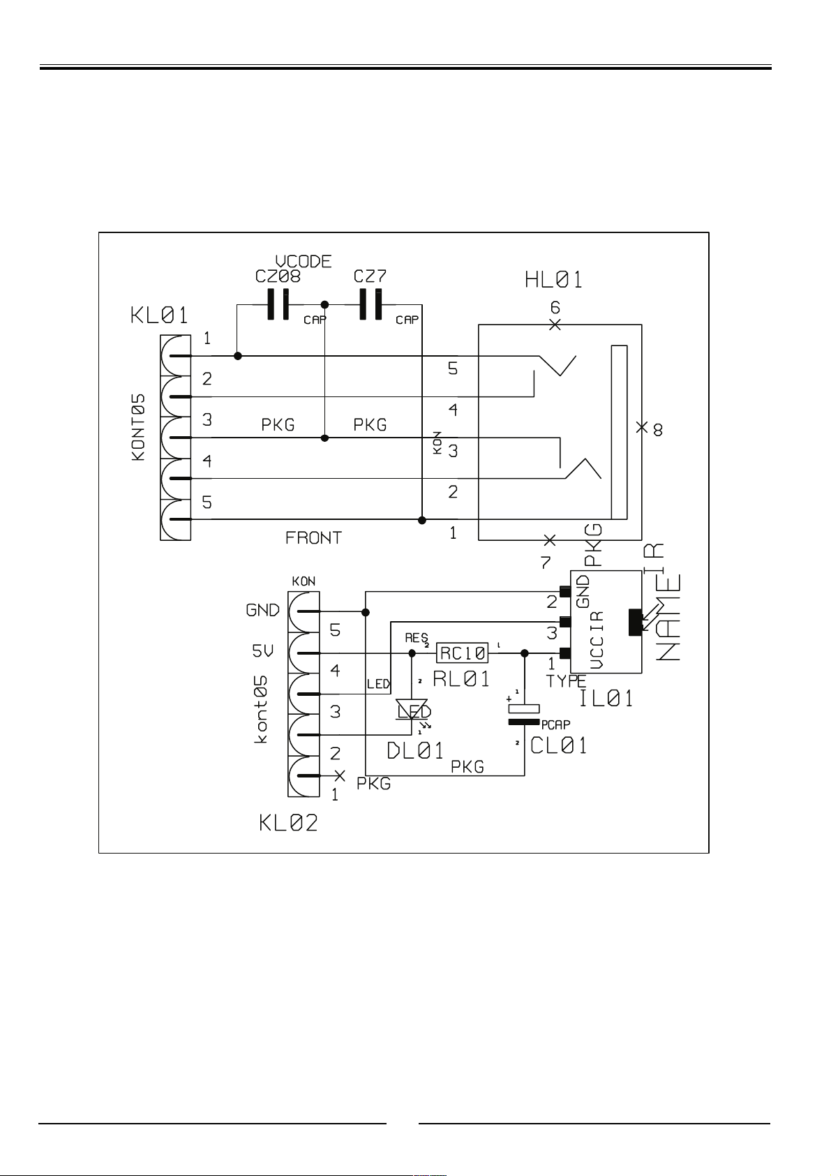
PT 90 NEAT Service Manual
A 15 IR MODULE
32
Page 33
R201
3.3V 3.3V 3.3V 3.3V3.3V
100K
PLLGND
PLLVCC
TC21
220U/16V
R203 51K
R207
R234 C208
C201
BC25
BC24
BC23
BC22
BC21
RA[0..9] 6,7
RA[0..9]
R204 4K7
C202
0.01U
R
AWRC 47K 10K
0.1U
PLLGND
0.1U
0.1U
0.1U
0.1U
0.1U
RN21
135
RA9
18P
C203
R
Default 47K 0.1U
ROEJ 7
RA8
RA7
RA6
RA5
RA4
RA0
RA1
RA2
RA3
TC22
RCASJ 7
RRASJ 7
642
3.3V
47U/16V
PT 90 NEAT Service Manual
DVD MODULE
XHD[0..15] 6
RD[0..15] 7
RD[0..15]
RWEJ 7
RFGND RFGND RFGND
XRD11
133
XRD4
134
XRD10
135
XRD5
136
XRD9
137
GND
138
XRD6
139
XRD8
140
XRD7
141
XRWEJ
142
XRSDCLK
143
XRRASJ
144
XRCASJ
145
VDD_3.3
146
XROEJ
147
XRA9
148
XRA8
149
VDD_3.3
150
XRA11
151
XRA10
152
XRA7
153
GND
154
XRA6
155
XRA5
156
XRA4
157
XRA0
158
XRA1
159
XRA2
160
XRA3
161
VDD_3.3
162
XTPLCK
163
XTSLRF
164
GND
165
XSPDIREF
166
XSFDIREF
167
AVDD5_PL
168
XSPLLFTR2
169
AVSS_PL
170
XSFDO
171
XSFTROPI
172
XSVR_PLL
173
174
XSVREFO
175
176
U21
RFGND
R208
C209
1000P
R231 R
RFO
RFO2
MVREF22,4
RD11
RD4
RD10
RD5
SRN33
R206 10K
0.1U
C205
0.1U
3.3V
PLCK
SLRF
C206
VC2
C208
47P
C207
RFVCC RFVCC RFVCC
RD9
RD6
RD8
RD7
0.1U
R207 47K
0.1U
PLLGND
BC26
BC27
BC28
PLLVCC
R234 R
PLLGND
0.1U
0.1U
0.1U
PLLGND
7 8
R205 5K1
R230 R
C204
XHD[0..15]
RD3
RD1
RD2
RD14
RD12
RD13
126
127
128
129
130
131
132
GND
XRD1
XRD2
XRD3
XRD14
XRD13
XRD12
XSPDOFTR1
XSAWRCVCO
XSDSSLV
XSRSLINT
VDD-3.3
AVSS_DS
XSRFIN
XSIPIN
AVDD5-DS
123456789
3.3V
RFVCC
R209 51K
C211
6800P
20K
C
C210
RFGND
R235 R
D21
TRAY_CNTL4
XHD11
XHD9
XHD5
XHD8
XHD6
XHD7
XHD10
RD0
RD15
118
119
120
121
122
123
124
125
XHD5
XHD9
XHD6
XHD8
XHD7
XRD0
XRD15
XSAWRC
XSRFGC
XSEFGC
XSFOCUS
XSTRACK
XSSLEG
AVDD5-DA
1011121314151617181920212223242526272829303132333435363738394041424344
MOTOR
TRACK
SLEG
FOCUS
TRAY_CNTL
3K3
3K3
10K
3K3
3K3
R213
R210
R214
R211
R212
12
1N4148
SSLEG4
EFGC2
STRACK4
SMOTOR4
SFOCUS4
XHD4
3.3V
3.3V
115
116
117
XHD4
XHD11
XHD10
XSMOTOR
AVSS-DA
XSRFRPLP
0
R228
MIRR2
RFRP2
C216
C215
C214
C213
C212
XHD12
XHD3
113
114
XHD3
XHD12
VDD_3.3
XSTELP
XSVREF2
XSRFRP
VC2
1000P
470P
470P
0.047U
0.47U
RFGND
XHD13
XHD2
112
XHD2
XSTEXI
C217
0.1U
111
XHD13
AVSS-AD
110
R215 47K
XHD1
109
GND
XSTEI
0
R216
XHD14
108
XHD1
XSFEI
SAEI
R217 R
MVREF22,4
XHD15
XHD0
106
107
XHD0
XHD14
XSAEI
AVDD5_AD
SSBAD
C218
TEXI2
HDRQ 6
IOWJ 6
104
105
XHD15
XHIOWJ
XHDRQJ
XSSBAD
GND
XSDFCT
DFCT
0.1U
R218 3K3
R219 4K7
TEI2
FEI2
IORJ 6
103
XHIORJ
XSCSJ
XSCSJ
C219
IORDY 6
HDACKJ 6
101
102
XHDACKJ
XHIORDYJ
XSCLK
XSDATA
XSDATA
XSCLK
1000P
C220
1000P
SAEI
R220 5K1
HINTJ 6
100
XHINTJ
XSLDC
XSFGIN
SAE2
HCS16J 6
HPDIAGJ 6
HA1 6
XHA1
XHCS16J
XHPDIAGJ
XSFGIN
XSSPDON
XSFLAG3
XSPDON
FLAG3
C221
HA0 6
HA2 6
XHA2
XHA0
XSFLAG2
XSFLAG1
FLAG2
FLAG1
0.1U
FLAG0
HDASPJ 6
HCS1J 6
HCS3J 6
XHCS3J
XHCS1J
XHDASPJ
XSFLAG0
XMP1_7
XMP1_6
BIT16
MP1_
RFGND
XMA15
GND
SSBAD
DFCT
SBAD2
8990919293949596979899
XMA13
XMA14
XMP1_5
XMP1_4
OUTSW
OUTSW4
XSCSJ
33
R221
SDFCT2
XSCLK
33
R222
SCSJ2
R236
XSDATA
33
R223
SCLK2
SDATA2
ALi M5705
GND
88
XMA12
87
XMA0
86
XMA1
85
XMA2
84
XMA3
83
XMA4
82
XMA5
81
XMA6
80
XMA7
79
XMA8
78
XMA9
77
VDD_3.3
76
XMA10
75
XMA11
74
XMINT1J
73
XMWRJ
72
XMRDJ
71
XMCSJ
70
XMD7
69
XMD6
68
XMD5
67
XMD4
66
XMD3
65
XMD2
64
XMD1
63
XMD0
62
GND
61
XOCS2
60
XOSC1
59
VDD_3.3
58
XMP1_0
57
XMALE
56
VDD_3.3
55
XMPSENJ
54
XCRSTJ
53
XGPIO0
52
XGPIO1
51
XHRSTJ
50
XMP1_1
49
XGPIO2
48
XMP1_2
47
XMFSCSJ
46
XMP1_3
45
RFGND
R
XSPDON
XSFGIN
SFGIN4
SSPDON4
INSW
INSW4
MFSCSJ5
3.3V
LED1
LED15
PLCK
PLCK
MA15
MA14
MA13
MA12
MA0
MA1
MA2
MA3
MA4
MA5
MA6
MA7
MA8
MA9
MA10
MA11
R237 0
SLRF
TP
SLRF
MD7
MD6
MD5
MD4
MD3
MD2
MD1
MD0
EJECT1
EJECT15
LDON2
TP
R226 10
R227 R
IDERST6
COUNTER
COUNTER
RFO
TP
FOCUS
FOCUS
RFO
MA[0..15] 5
MA[00..15]
CRSTJ4,5
PI_SIGO2
TP
TRACK
TP
TP
SLEG
SLEG
TRACK
J21
MWRJ 5
MPSENJ5
MOTOR
TP
SSBAD
TP
SSBAD
MOTOR
123
A16J5
DFCT
TP
DFCT
VCCTXRX
VCC
L21
TP
XSFGIN
TP
XSFGIN
FLAG0
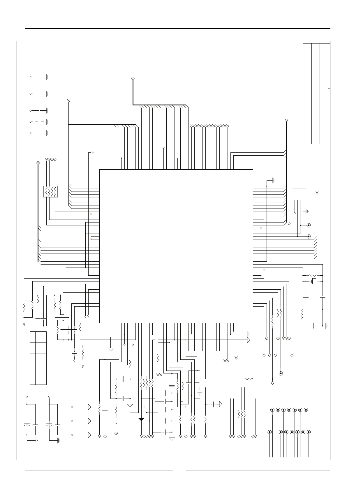
ALI M5705 (176 PIN) DVD/CD DECODER
DECODER.SCH
Title
MD[0..7] 5
GND
RS232
4
MD[0..7]
RXD
TP
TXD
TP
R229
100K
Y21
C225
12P
TP
FLAG3
TP
FLAG3
C224
C
12P
33.8688MHz
FLAG0
TP
FLAG1
FLAG1
C223
L
FLAG2
TP
FLAG2
33
Page 34
PT 90 NEAT Service Manual
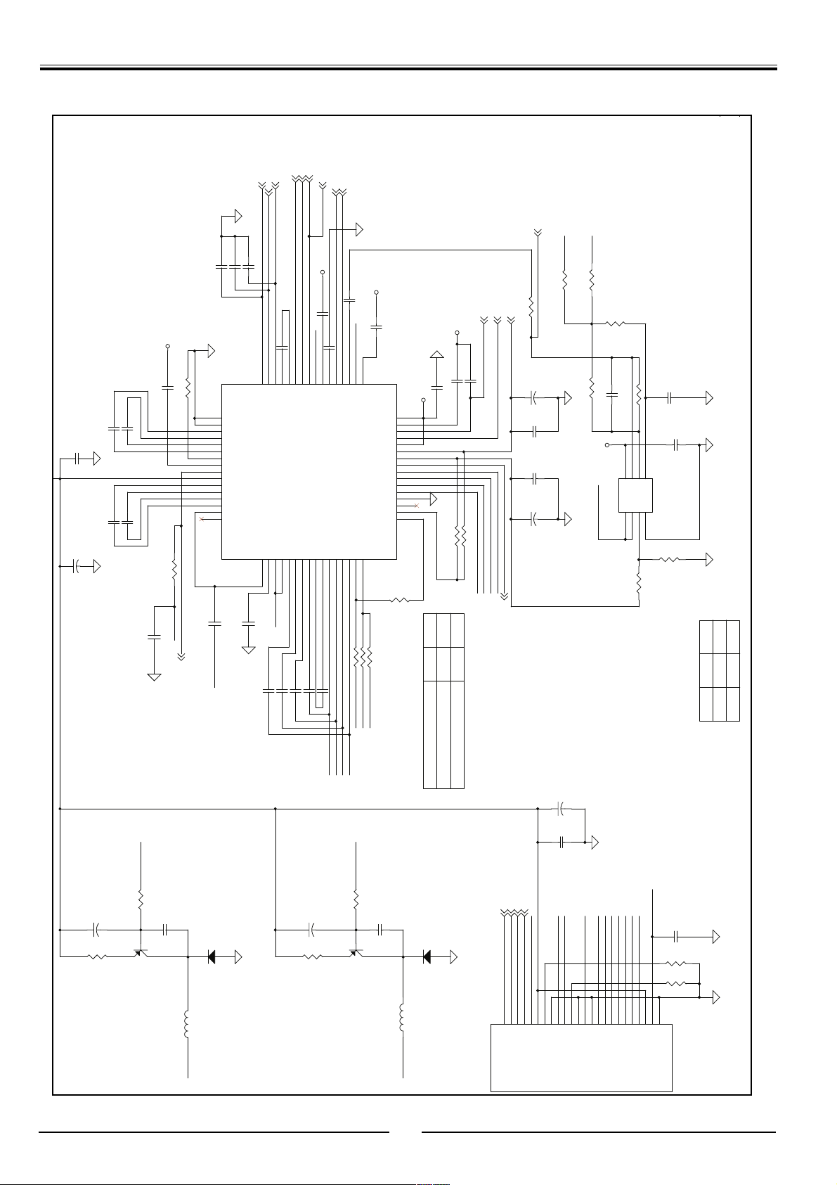
ALI HOP 1000 PRE-AMP CIRCUIT
ALI HOP-1000
PRE-AMP.
RFVCC
C107
0.1U
R104
8K2
C103
0.1U
C105
0.1U
0.1U
BC11
RFGND
C102
0.1U
C104
0.1U
TEI 3
SAE 3
FEI 3
SCSJ 3
SCLK 3
SDATA 3
RFGND
C110
33P
C111
33P
C113
33P
C116
RFGND
U11
49
50
51
52
53
54
55
56
57
58
59
60
61
62
63
64
484746454443424140393837363534
SCLK
SDEN
SDATA
HOLD1
VNA
FNN
FNP
DIP
DIN
RX
BYP
SIGO
VPA
AIP
AIN
ATON
ATOP
CDRF
CDRFDC
LCP
0.047U
LCN
TEXI 3
SDFCT 3
SBAD 3
PI
MIRR 3
MVREF2 3,4
MVREF2
R112 R
TC15
C128
C127
TC14
RFRP 3
100U/16V
0.1U
0.1U
100U/16V
MEVO
R113 0
RFGNDRFGND
PI
R114 R
10K
R136
MVREF2
R115
C131
RFVCC
U12
470K
33P
V+
AOA-A+
123
PREAMP.SCH
Title
56K
C134
0.47U
TL3472
BC13
0.1U
RFGND
R118
678
B-
BO
V- B+
4 5
RFGND
RFVCC
RFVCC
C
C122
C120
1000P
C121
FEI
MEI-
TE
FE
CE
MEI
TPH
MEV
SP3721
0.1U
DFT
C123
150P
33
PI
MIN
MLPF
MEVO
FDCHG
MB
MP
MIRR
VPB
VCI
VC
LDON
CDLD
CDPD
DVDLD
DVDPD
VNB
NC
VC12
CDTE
RFVCC
BC12 0.1U
32
31
30
29
28
27
26
25
24
23
22
21
20
19
RFGND
18
17
RFGND
C125
RFVCC
4700P
C126
EFGC 3
1000P
TC11
220U/16V
TC12
R101
RFGND
100U/16V
10
3.3P
C101
RFGND
CDLDO
R102
5K1
C106
EBC
Q11
SOT89EBC 2SB1132
4K7
R103
MEI-
1000P
DVDFRP
DVDRFN
PD1
PD2A2B2C2D2CPCNDCBAFE
123456789
MVREF25
C112
RFGND
1 2
RFGND
0.1U
C114
680P
C109 680P
RFO3
PUHRF
D11
1N4148
L11
10UH
CDLD
C115
680P
C117
680P
10111213141516
C118
680P
C119
100U/16V
TC13
R105
10
100P
D
C
B
R107 1K2
R108 1K2
R109 10K
E
MVREF25
A
DVDLDO F MEVO
R106
1K
EBC
Q12
SOT89EBC 2SB1132
C124
1000P
R110
L12
10K
10UH
DVDLD
R134 0
R135 R
MVREF25
DVDMDI
DVDLDO
CDMDI
CDLDO
R
0
0
R134 R135
MVREF2=MVREF25 R
MVREF2!=MVREF25
1 2
RFGND
D12
1N4148
CN11
R132
LDON3
TC16
100U/16V
C129
0.1U
RFGND
TRACK- 4
TRACK+ 4
FOCUS- 4
FOCUS+ 4
DVDLD
CDLD
CDMDI
LD(CD)
LD(DVD)
VR
GND(NC)
PUHRFCBADFE
C
PD
GND
RFOUT
F
B
A
D
TRACK-
TRACK+
FOCUS-
FOCUS+
DVDMDI
24232221201918171615141312111098765432
VR
FO-
TR+
TR-
FO+
VCC
GND
PD(MONITOR)
1K5
MVREF25
E
VCC
R133
8K2
C130
R123
R122
1
GND
VS(VCC)
HOP-1000 JP24-05M
RFGND RFGND
Vref R132 R133
2.1V 1.5K 8.2K
2.5V 0 R
0.1U
100
100
RFGND RFGND
34
Page 35
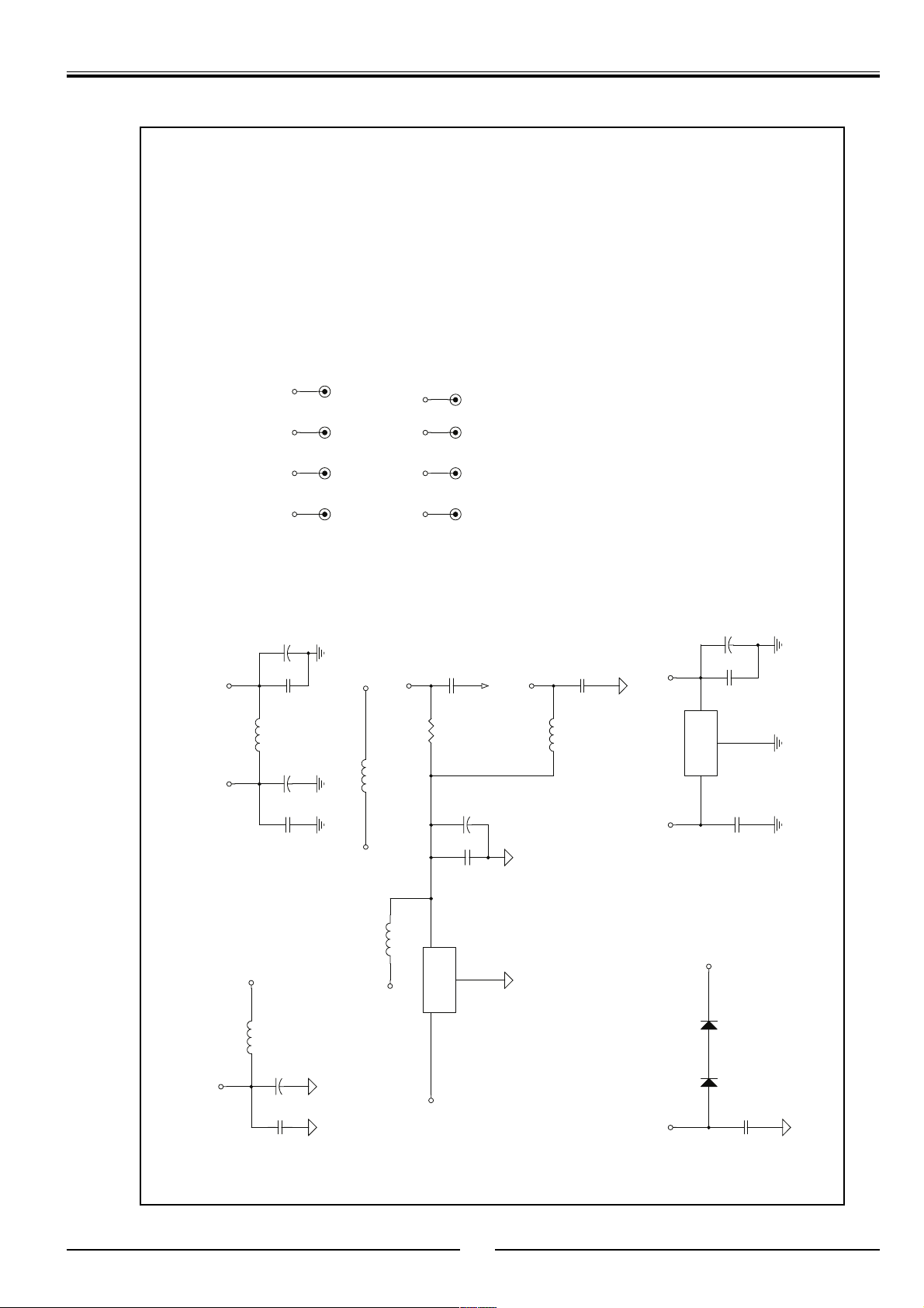
ALI HOP-1000
POWER
PT 90 NEAT Service Manual
VCC
5V
3.3V
RFVCC MVCC
PLLVCC
100U/16V
TC73
C703
0.1U
L72
FB-1
1 2
TC72
220U/16V
C702
0.1U
TP
3.3V
TP
MVCC
TP
RFVCC
TP
PLLVCC
L74
1 2
M5V
FB-1
PLLVCC
RFGND MGNDPLLGND GND
R701
C704
0.1U
3.3 0805
TC75
TP
GND
TP
MGND
TP
RFGND
TP
PLLGND
220U/16V
PLLGND
RFVCC
100U/16V
TC76
C707
0.1U
Q72
SOT223 AS1117
IN OUT
3 2
GND
C708
1
C709
0.1U
0.1U
RFGND
L77
FB-1
1 2
5V 3.3V
12V
5V
C706
L78
FB-1
3
+12V
5V
L71
FB-1
220U/16V
TC71
PAGNDPAGND
C701
0.1U
Q73
(BA05 TO252AA)
2
1
MVCC
0.1U
PAGND
PAGND
12V
D72
D71
MVCC
1 2
1 2
1N4002
1N4002
C710
0.1U
PAGND
35
Page 36
PT 90 NEAT Service Manual
HA1/AUX4[3]
VSS
HA0/AUX4[2]
HCS3FX#/AUX3[6]
HCS1FX#/AUX3[7]
152
153
154
155
156
VEE
HA2
/AUX4[4]
VEE
AUX[0]
AUX[1]
AUX[2]/IOW#
VSS
VEE
AUX[3]/IOR#
AUX[4]
AUX[5]
AUX[6]
AUX[7]
LOE#
VSS
VCC
LCS0#
LCS1#
LCS2#
LCS3#
VSS
VEE
VSS
LD10
LD11
VSS
VEE
LD12
LD13
LD14
LD15
LWRLL#
LWR HL #
VSS
VEE
CAMIN0
CAMIN1
VSS
LD0
LD1
LD2
LD3
LD4
LD5
LD6
LD7
LD8
LD9
LA0
LA1
LA2
LA3
157
158
159
160
161
162
163
164
165
166
167
168
169
170
171
172
173
174
175
176
177
178
179
180
181
182
183
184
185
186
187
188
189
190
191
192
193
194
195
196
197
198
199
200
201
202
203
204
205
206
207
208
1
2 3 4 5 6 7 8 910111213141516171819202122232425262728293031323334353637383940414243444546474849505152
HIOCS16#/CAMCLK/AUX3[4]
HWR#/DCI_CLK/AUX4[5]
HRD#/DCI_ACK#/AUX4[6]
VEE
VSS
HIORDY/AUX3[3]
HIRQ/DCI_ERR#/AUX4[7]
HRST#/AUX3[5]
HRRQ#/AUX4[0]
143
144
145
146
147
148
149
150
151
VSS
HD13/AUX2[5]/SP
HD12/AUX2[4]/C2PO
HD11/AUX2[3]//IRQ
HD10/AUX2[2]/SQSK
HD9/AUX2[1]/SQSO
HWRQ#/DCI_REQ#/AUX4[1]
HD15/AUX2[7]/IR
HD14/AUX2[6]/SQSI
VCC
137
138
139
140
141
142
HD8/DCI_FDS#/AUX2[0]/VFD_CLk
HD7/DCI7/AUX1[7]/ VFD_DIN
131
132
133
134
135
136
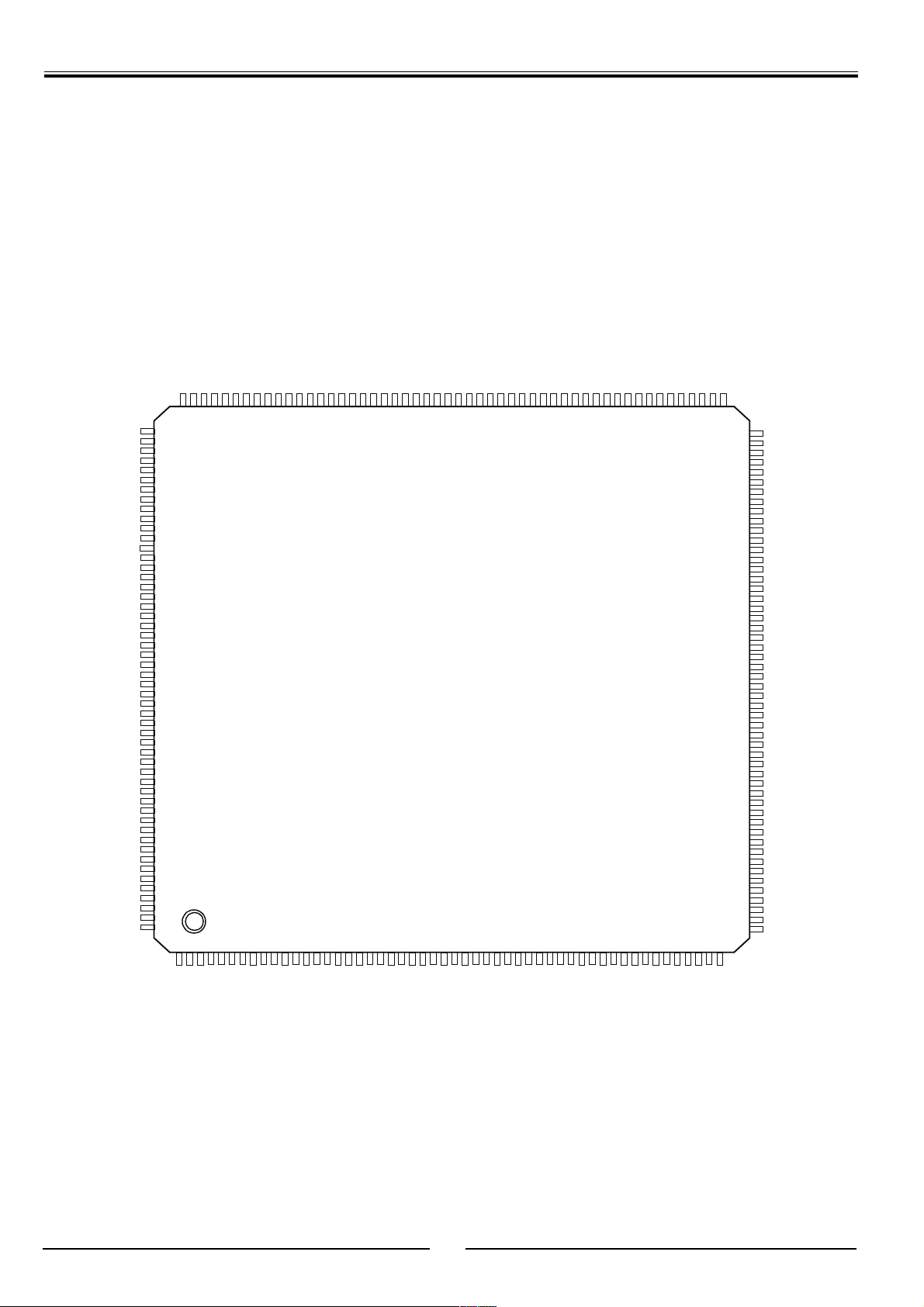
ES6008/18/28/38
208-Pin PQFP Package
VEE
130
VSS
129
HD4/DCI4/AUX1[4]
HD5/DCI5/AUX1[5]
HD6/DCI6/AUX1[6]/VFD_DOUT
HD2/DCI2/AUX1[2]
HD3/DCI3/AUX1[3]
HD1/DCI1/AUX1[1]
HD0/DCI0/AUX1[0]
VCC
VSS
HSYNC#/CAMIN7/AUX3[0]
PCLK2XSCN/CAMIN4
YUV7/CAMIN3
YUV6/VDAC
PCLKQSCN/CAMIN5/AUX3[2]
VSYNC# /CAMIN6/ AUX3[1]
118
119
120
121
122
123
124
125
126
127
128
YUV5/YDAC
VSS
ADVEE
YUV4/RSET
YUV3/COMP
YUV2/CDAC
YUV1/VREF
YUV0/CAMIN2/UDAC
DCLK
105
106
107
108
109
110
111
112
113
114
115
116
117
104
103
102
101
100
57
99
98
97
96
95
94
93
92
91
90
89
88
87
86
85
84
83
82
81
80
79
78
77
76
75
74
73
72
71
70
69
68
67
66
65
64
63
62
61
60
59
58
56
55
54
53
VEE
VSS
DSCK
DQM
DCS0#
VEE
VSS
DCS1#
DB15
DB14
DB13
DB12
VEE
VSS
DB11
DB10
DB9
DB8
DB7
DB6
VSS
VCC
DB5
DB4
DB3
DB2
DB1
DB0
VSS
VEE
DMBS1
DMBS0
DRAS#
DWE#
DOE#/DSCK_EN
DCAS#
VEE
VSS
DMA11
DMA10
DMA9
DMA8
DMA7
DMA6
VSS
VEE
DMA5
DMA4
DMA3
DMA2
DMA1
DMA0
VEE
LA4
LA5
LA6
LA7
LA8
LA9
VSS
VCC
VCC
RSD
NC
XIN
XOUT
AVEE
VSS
RWS
RBCK
NC
VSS
LA11
LA10
LA12
LA13
VEE
LA14
LA15
LA16
LA20
LA17
LA18
LA19
LA21
RESET#
TDMDX/RSEL
VSS
VEE
TDMDR
TDMCLK
VSS
VCC
TSD2
TDMFS
TDMTSC#
TWS/SEL_PLL2
TSD0/SEL_PLL0
TSD3
TSD1/SEL_PLL1
VSS
TBCK
MCLK
SPDIF/PLL3
MPEG Board
MPEG Decoder
36
Page 37

PT 90 NEAT Service Manual
11- DESCRIPTION
OF INTEGRATED
CIRCUITS
-TV PART-
37
Page 38
PT 90 NEAT Service Manual
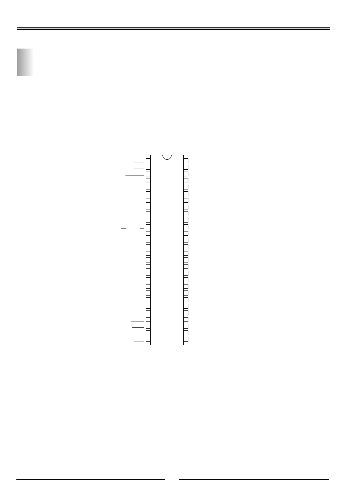
STV224X pos: ICV1
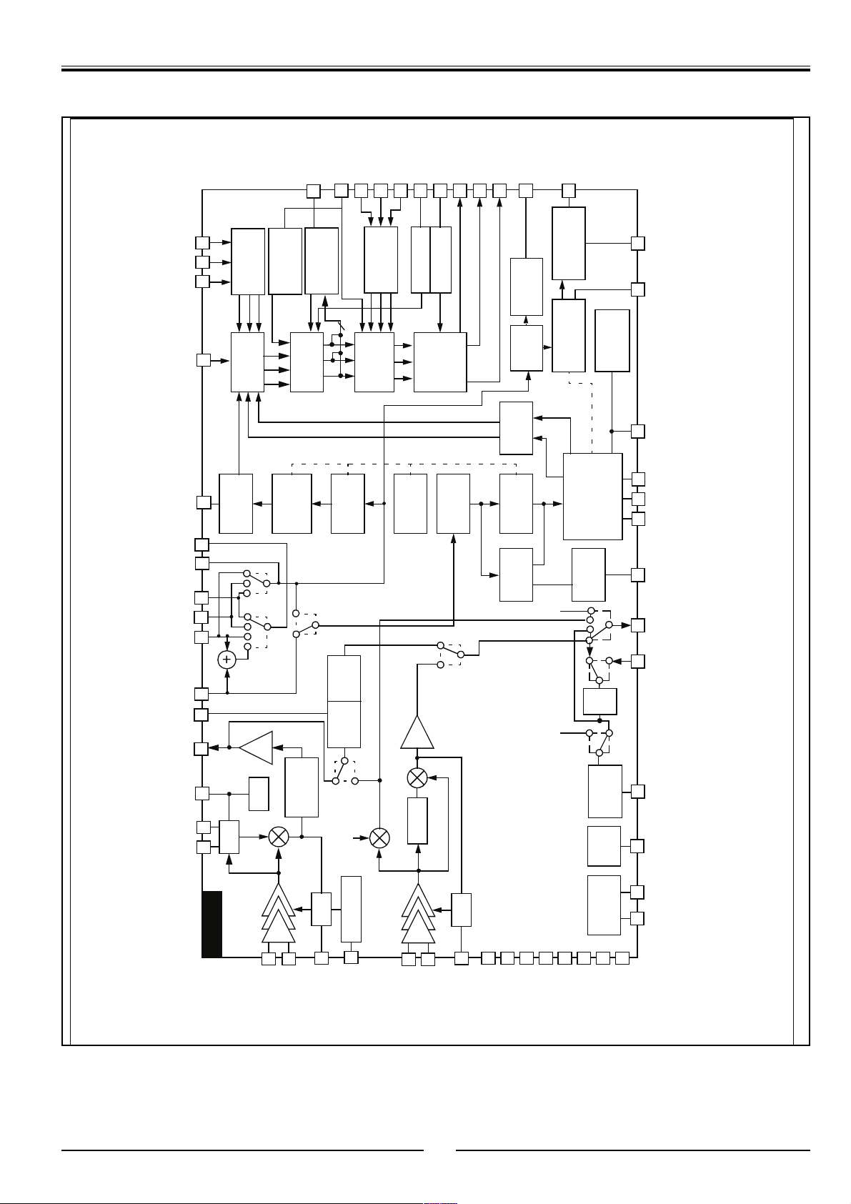
Multi Standard TV Processor
STV224X is a fully bus controlled IC for TV including PIF, SIF , Luminance , Chrominance and deflection processing. It is a
bus controlled PAL / SECAM / NTSC single chip TV Processor. For details of STV224X features please refer to the
STV224X datasheet. 110° , 4:3 or 16:9 CRT applications. It integrates both vertical deflection and E-W correction circuit
necessary for design of 110° chassis it allows designing a PAL/NTSC(BGDKIMN) set with very few external components
and no manual adjustment.
SIFIN1
SIFIN2
AGCSIFCAP
V
AGCPIFCAP
PIFIN1
PIFIN2
TUNERAGCOUT
IFPLL
GND
AM /FMOUT/SC
V
INTCVBSOUT
EXTAUDIOIN
PIFLC1
PIFLC2
CVBSIN1
GND2
CVBSIN2
Y/CVBSIN3
BEXT/Cb
GEXT/Y
REXT/Cr
FBEXT
REFIF
CCIF
V
CC2
BS
CHR
APR
1
2
3
4
5
6
7
8
9
10
IF
11
12
13
14
15
16
17
18
19
20
21
22
23
24
25
26
27
28
56
55
54
53
52
51
50
49
48
47
46
45
44
43
42
41
40
39
38
37
36
35
34
33
32
31
30
29
FMCAP
AUDIOOUT
GNDD
V
CCD
SDA
SCL
SLPF
LFB/SSC
HOUT
VERT
BCL/SAF
V
CC1
CVBSOUT2
GND1
X1/VAMP/CHROUT
CLPF
XTAL1
XTAL2
XTAL3/BTUN
FBOSD/HC
ROSD
GOSD
BOSD
I
CATH
ROUT
GOUT
BOUT
NTBC/CVBSOUT1
38
Page 39
t
STV224X
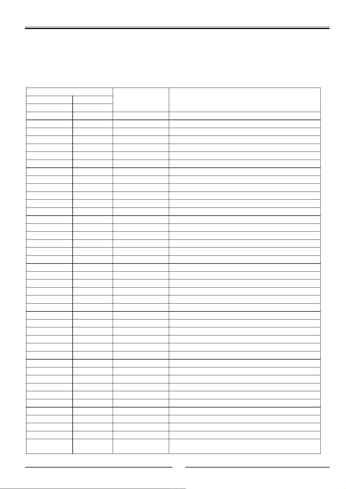
1.2 PIN DESCRIPTION
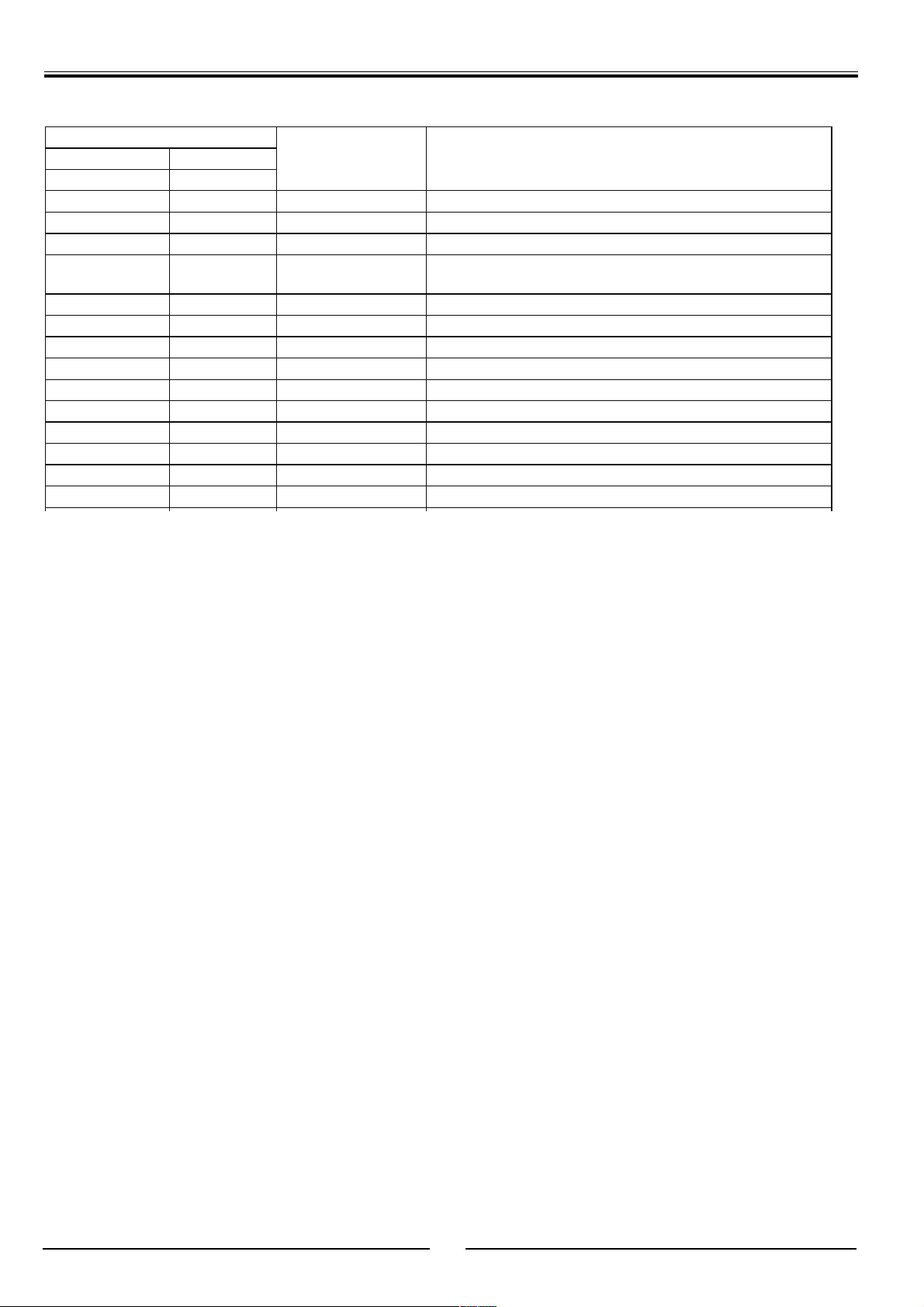
Table 1. Pin Configuration
Pin N°
SDIP56 TQFP64
18SIFIN1 SIFInput
29SIFIN2 SIFInput
310AGCSIFCA P AG C SIF C apacitor
411V
5 12 AGCPIFCAP AGC PIF Capacitor
6 13 PIFIN1 PIF Input
7 14 PIFIN2 PIF Input
8 16 TUNERAGCOUT AGC Tuner Output
9 17 IFPLL IF PLL Filter
10 18 GND
11 19 AM/FMOUT/SC AM/FM Mono Sound or Stereo Carriers Output
12 20 V
13 21 INTCVBSOUT Internal CVBS Output
14 22 EXT AUDIOIN External Audio Input
15 23 PIFLC1 LC Input
16 24 PIFLC2 LC Input
17 25 V
18 26 CVBSIN1 Internal Video Input
19 27 GN D 2 Video/Luma Ground
20 28 CVBSIN2 External Video Input
21 29 BS Black Stretch Capacitor
22 34 Y/CVBSIN3 Y(SVHS) or CVBS3 External Input
23 35 CHR Chroma (SVHS) Input
-37UINB-Y Input
-38VINR-Y Input
-39YINYInput
- 40 YOUT Y Output
-41VOUT R-YOutput
-42UOUT B-YOutput
30 43 BOUT Blue Output
31 44 GOUT Green Output
32 45 ROUT Red Output
33 46 I
34 47 BOSD OSD Blue Input
35 48 GOSD OSD Green Input
36 49 ROSD OSD Red Input
37 50 FBO SD/HC OSD Fast BlankingInput / Half Contrast onSD IP56 package
38 52 XTAL3/BTUN 3.5X M Hz C rystalorCloche FilterTuningC apac itor
39 53 XTAL2 3.5X MHz Crystal
40 54 XTAL 1 4.43 /3. 5X MHz Cryst al
41 55 CLPF Chroma PLL Filter
42 56 X1/VAMP/CHROUT
REFIF
CCIF
CC2
CATH
IF
PT 90 NEAT Service Manual
Symbol DescriptionSTV224XC/8XC STV223XD
Voltage Reference Filtering
IF Ground
5 V IF Supply
Video/Luma Supply Voltag e (8 V)
Cathode Current Measurement Input
XTAL1 Control Pin, Vertical Amplitude DAC Outpu
Chroma Reference Signal Output
39
Page 40
PT 90 NEAT Service Manual
PinN°
SDIP56 TQFP64
43 57 GND1 Chroma/Scanning Ground
- 58 CVBSOUT1 Main Video Switch Output
45 59 V
46 61 BCL/SAF
47 62 VERT Vertical Output Pulse
48 63 HOUT Horizontal Output Pulse
49 64 LFB/SSC Line Flyback Input and Super-Sandcastle Output
50 1 SLPF Scanning PLL Filter
51 2 SCL I C Bus Clock Input
52 3 SDA I C Bus Data Input
53 4 V
54 5 GNDD Digital Ground
55 6 AUDIOOUT Main Audio Output
56 7 FM CAP FM D em odulation Capacitor
CC1
CCD
Symbol DescriptionSTV224XC/8XC STV223XD
Chroma/Scanning Power Supply (8 V)
Beam Current Limiter Control Voltage and Safety
(XRAY)
Digital Supply Voltage (5 V)
40
Page 41
PT 90 NEAT Service Manual
REXT/Cr
GEXT/Y
BEXT/Cb
FBEXT
CVBSOUT2
NTBC/CVBSOUT1
CVBSIN1
CVBSIN2
Y/CVBSIN3
CHR
FMCAP
INTCVBSOUT
BS
APR
24
27
26
RGB
HALF
25
28
21
44
29
18
20
22
TO YUV
CONTRAST
YUV
SWITCH
BLACK
STRETCH
MATRIX
SAT./CONT
LUMA DL
PEAKING
& CORING
APR
FBOSD/HC
37
3
ROSD
363534
TRAP
CHROMA
GOSD
RGB
CONTRAST
RGB
SWITCH
FM
SOUND BP
DEEMP.
FM DEMOD
23
56
13
BOSD
Mono
FILTER
TUNING
CATH
BCL/SAF
I
463332
SENSE
BCL/SAF
CATH
I
DRIVE
BRIGHT.
CUTOGG
BLANKING
ACC & ACC
OVERLOAD
AM
Mono
ROUT
GOUT
31
Sound
Subcarrier
BOUT
VERT
30
47
VERTICAL
SYNC.
DL
CHROMA
FILTER
BANDPASS
FILTER
CLOCHE
SCANNING
SEP
HOUT
48
2nd LOOP
HORIZONTAL
1st LOOP
HORIZONTAL
AUTO IDENT.
CLOCHE
VAM P DC
KILLER
DEMODULATOR
PAL/SECAM/NTSC
TUNING
LFB/SSC
49
SLPF
50
CONTROL
X1/VAMP/CHROUT
42
CLPF
41
XTAL1
XTAL2
XTAL3/BTUN
38111455
Mute
AM/FMOUT/SC
EXTAUDIOIN
AVL
Mute
IFPLL
PIFLC2
PIFLC1
9
16
15
AFC
W/B SPOT
INVERTER
PLL
Carrier
LIMITER
PLL Reference
VOLUME
AUDIO
AUDIOOUT
V
4
REF
REF
SCL
AGC
TUNER AGC
STV2248
7
PIFIN26PIFIN1
8
5
1
SIFIN12SIFIN2
AGCPIFCAP
AGC
3
AGCSIFCAP
53
V
CCD
IC BUS
54
10
54
45
43
V
CC1
GND1
17
CC2
V
IF
CCIF
V
GNDD
GND
SDA
52 51
DECODER
19
GND2
TUNERAGCOUT
41
Page 42

PT 90 NEAT Service Manual
MAIN FEATURES
l I-C bus control (read and write modes),
l PIF PLL demodulator, Bus controlled VCO alignment,
l IF positive and negative modulation,
l Digital AFC,
l Tuner delayed AGC output,
l White and Black spot cancellation,
l SIF with QSS or intercarrier structure,
l Built in sound bandpass,
l Multistandard PLL FM demodulator (4.5, 5.5,
6.0,6.5MHz),
l AM demodulator for France,
l FM sound carriers output for Stereo chassis,
l Audio switch for external audio input, Mono chassis,
l Digital volume control,
l Audio Mute,
l Video switch, 3 CVBS inputs, 1 CVBS output which can
be used to drive teletext decoder,
l SVHS switch, Y input is combined with CVBS3 input,
l OSD RGB analog inputs, fast blanking detection on OSD
fast blanking pin, contrast control capability,oversize
blanking capability on OSD fast blanking input,
l External analog RGB inputs with contrast and saturation
control (external RGB matrixed in YUV).
l Integrated chroma filters (trap, bandpass, cloche) with
automatic alignment,
l Integrated luminance delay line,
l Adjustable peaking on the luminance signal with coring
function,
l Black strech circuit,
l PAL / SECAM / NTSC color decoder with automatic iden-
tification of standards,
l Integrated chroma delay line,
l Full integrated SECAM decoder,
l Hue control, two selectable matrixes in NTSC mode,
l Automatic flesh control circuit with two selectable charac-
teristics (normal and wide),
l ACC overload circuit,
l Chroma subcarrier output, which could be used to drive
comb filter circuit,
l Automatic RGB peak regulation (APR).
l Automatic digital cut-off current loop with warm-up detec-
tion circuit,
l White point and cut-off point adjustments,
l Beam current limiter control stage,
l High performance synchronization pulses separator,
l Horizontal synchronization with two phase locked loops,
l Integrated VCO, auto-calibration using the chroma crystal
reference frequency,
l Automatic time constant selection for the first PLL, 3
selectable time constants,
l Video identification circuit (independent from PLL1),
l Noise detector circuit,
l Vertical countdown circuit,
l Automatic 50/60Hz selection circuit,
l Blanking and inserted cut-off pulses position adapted to
standard (50 or 60Hz),
l Long blanking mode capability in 60Hz (same blanking as
50Hz standard),
l Possibility to insert cut-off pulses after a vertical oversize
blanking signal,
l De-interlace capability,
l Horizontal starting circuit with soft-start capability,
l Horizontal and vertical position adjustments, vertical
amplitude control voltage (combined with chroma subcarrier output),
l 4/3, 16/9 selection voltage.
42
Page 43
PT 90 NEAT Service Manual
m
V
m
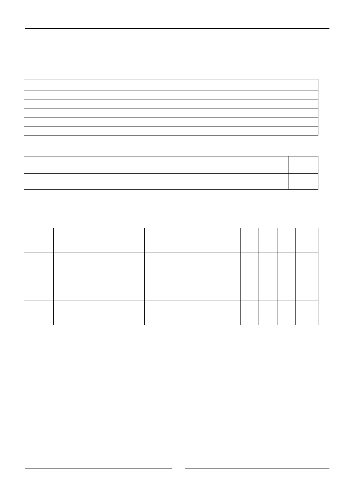
ELECTRICAL CHAR ACTERISTICS
ABSOLUTE MA XIMUM RA TING S
Symbol Parameter Value Unit
V
_8V
CC
V
CC
V
ESD
T
oper
T
stg
THE RM A L DA TA
8 V Supply Voltage 10 V
_5V
5 V Supply Voltage 7 V
Capacitor 100 pF discharged via 1.5 k serial resistance (Human Body Model)
±2
Operating Te m pe ra ture 0, +70 °C
Storage Temperature -55, +150°C
kV
Symbol Parameter
R
th (j-a)
Junction-ambient Thermal Resistance (measured at P
=1W)
D
SDIP56 40 °C/W
TQFP64 50 °C/W
Typical
Value
Unit
SUPPLY
(Supplies at T ypical Values, T
= 25° C, IC bus register at power-on res et value, auto
amb
mode, unless otherwise specified).
Symbol Parameter Test Conditions Min. Typ Max. Unit
V
CCIF
V
CCD
V
V
I
CCIF
I
CC5F
I
CCI
I
CC2
P
CC1
CC2
IF Circuit Supply Voltage 4.75 5 5.25
Bus & Digital Supply Voltage 4.75 5 5.25
Chroma, Scanning Supply Voltage 7.6 8 8.4
Video Supply Voltage 7.6 8 8.4 V
V
Current Consumption V
CCIF
V
Current Consumption V
CC5F
V
Current Consumption V
CCI
V
Current Consumption V
CC2
TotalPower Dissipation
D
= 5 V. No -l o ad at RGB outputs . 58
CCIF
= 5 V. No-load at RGB outputs. 48 m
CCD
= 8 V. No-load at RGB outputs. 40 m
CCI
= 8 V. No-load at RGB outputs. 56 m
CC2
V
= V
CCI
V
CCIF =VCC5V
CC2
= 8 V,
= 5 V
1300 mW
No-load at RGB out pu ts.
43
Page 44

PT 90 NEAT Service Manual
ST92195C/D pos: IC01
48-96 KB ROM HCMOS MCU WITH ON-SCREEN DISPLAY AND
TELETEXT DATA SLICER
General Features:
•
Register File based 8/16 bit Core Architecture with RUN,
WFI, SLOW and HALT modes
•
0°C to +70°C Operating Temperature Range available
•
Up to 24 MHz Operation @ 5V±10%
•
Minimum instruction cycle time: 165nS at 24MHz.
•
48, 56, 64, 84 or 64K Bytes ROM
•
256 Bytes RAM of Register file (accumulators or index
registers)
•
256 to 512 Bytes of on-chip static RAM
•
2 or 8 Kbytes of TDSRAM (Teletext and Display Storage
RAM)
•
28 fully programmable I/O pins
•
Serial Peripheral Interface
•
Flexible Clock controller for OSD, Data Slicer and Core
clocks running from
a single low frequency external crystal.
•
Enhanced Display Controller with 26 rows of 40/80 char-
acters
– 2 sets of 512 characters
– Serial and Parallel attributes
– 10x10 dot Matrix, definable by user
– 4/3 and 16/9 supported in 50/60HZ and 100/120 Hz
mode
– Rounding, fringe, double width, double height,
scrolling, cursor, full Background color, half-intensity
color, translucency and half-tone modes
•
Teletext unit, including Data slicer, Acquisition Unit and
up to 8K Bytes RAM for Data Storage
•
VPS and Wide Screen Signalling slicer
•
Integrated Sync Extractor and Sync Controller
•
14-bit Voltage Synthesis for tuning reference voltage
•
Up to 6 External Interrupts plus one non-maskable inter-
rupt
•
8 x 8-bit programmable PWM outputs with 5V open-drain
or push-pull capability
•
16-bit Watchdog timer with 8-bit prescaler
•
1 or 2 16-bit standard timer(s) with 8-bit prescaler
•
I–C Master/Slave (on some devices)
•
4-channel A/D converter; 5-bit guaranteed
•
Rich instruction set and 14-Addressing modes
•
Versatile development tools, including Assembler, Linker,
C-Compiler, Archiver, Source Level Debugger and hardware emulators with Real-Time Operating System available from third parties
•
Pin Compatible EPROM and OTP devices available.
Microcontroller+OSD+(Teletext decoder)+VPS/PDC/WS
decoder are embedded in one chip, where there are two
types with the major difference;
ST92185 No-teletext
ST92195 With teletext
The ST92195 microcontroller is developed and manufactured by STMicroelectronics using a pro-prietary n-well
HCMOS process. Its performance derives from the use of
a flexible 256-register pro-gramming model for ultra-fast
context switching and real-time event response. The intelligent on-chip peripherals offload the ST9 core from I/O and
data management processing tasks allowing critical application tasks to get the maximum use of core resources.
The ST92195 MCU supports low power consumption and
low voltage operation for power-efficient and low-cost
embedded systems.
The advanced ST9+ Core consists of the Central Processing Unit (CPU), the Register File and the Interrupt controller. The general-purpose registers can be used as accumulators, index registers, or address pointers. Adjacent
register pairs make up 16-bit registers for addressing or
16-bit processing. Although the ST9 has an 8-bit ALU, the
chip handles 16-bit operations, including arithmetic,
loads/stores, and memory/register and memory/memory
exchanges. Two basic addressable spaces are available:
the Memory space and the Register File, which includes
the control and status registers of the on-chip peripherals.
Power consumption of the device can be reduced by more
than 95% (Low power WFI).
Up to 28 I/O lines are dedicated to digital Input/Output.
These lines are grouped into up to five I/O Ports and can
be configured on a bit basis under software control to provide timing, status signals, timer and output, analogue
inputs, external interrupts and serial or parallel I/O. A set
of on-chip peripherals form a complete system for TV set
and VCR applications:
– Voltage Synthesis
– VPS/WSS Slicer
– Teletext Slicer
– Teletext Display RAM
– OSD
44
Page 45
PT 90 NEAT Service Manual
c
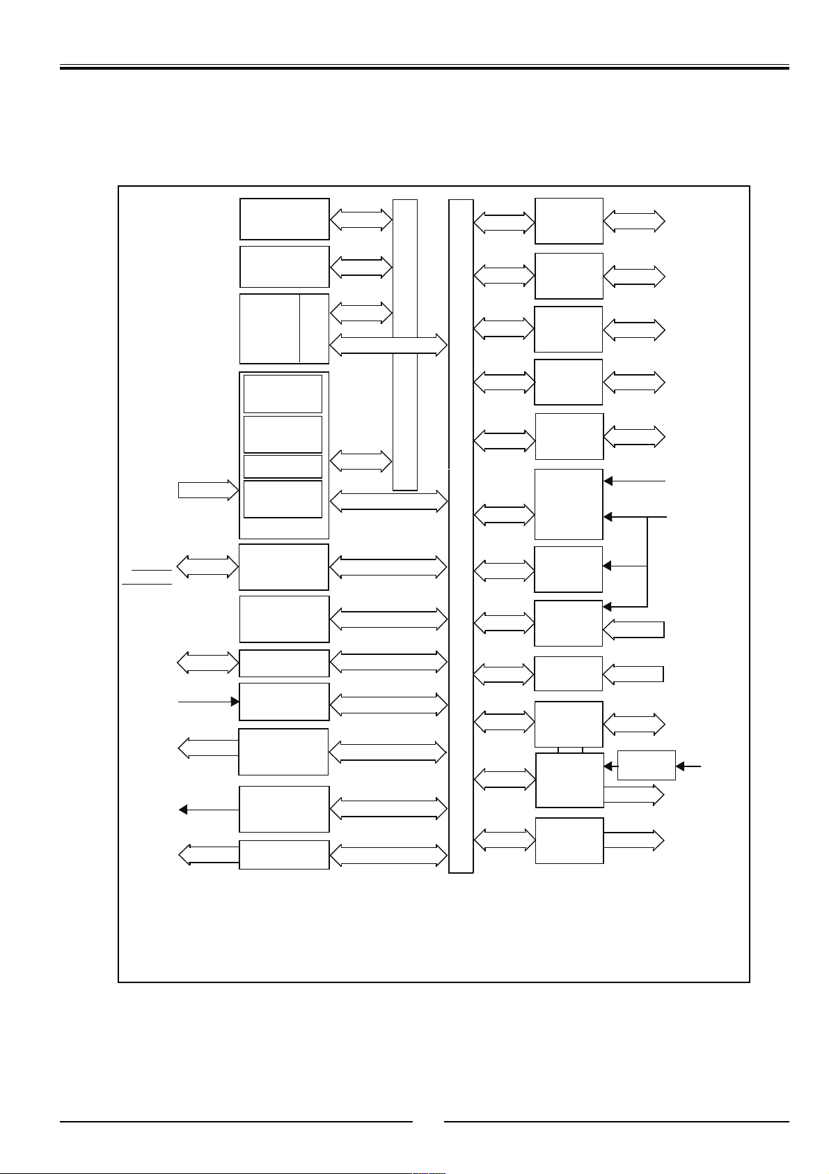
BLOCK
DIAGRAM
NMI
INT[7:4]
INT2
INT0
OSCIN
OSCOUT
RESET
RESETO
SDO/SDI
SCK
MCFM
VSO[2:1]
STOUT0
DA1/SCL1
DA2/SCL2
Up to 96
Kbytes ROM
256 or 512
bytes RAM
Up to 8
Kbytes
TDSRAM
256 bytes
Register File
Interrupt
Management
ST9+ CORE
WATCHDOG
TIMING AND
CLOCK CTRL
VOLTAGE
SYNTHESIS
STANDARD
TIMER
TRI
8/16-bit
CPU
MMU
RCCU
16-BIT
TIMER/
SPI
1)
2)
IC
I/O
PORT 0
I/O
PORT 2
I/O
PORT 3
I/O
PORT 4
I/O
MEMORY BUS
REGISTER BUS
PORT 5
DATA
SLICER
& ACQUI-
SITION
UNIT
SYNC.
EXTRAC-
TION
VPS/WSS
DATA
SLICER
ADC
SYNC
CONTROL
ON
SCREEN
DISPLAY
PWM
D/A CON-
VERTER
MULTIP.
8
6
4
8
2
FREQ.
P0[7:0]
P2[5:0]
P3[7:4]
P4[7:0]
P5[1:0]
TXCF
CVBS1
WSCR
WSCF
CVBS2
AIN[4:1]
EXTRG
VSYNC
HSYNC/CSYNC
CSO
PXFM
R/G/B/FB
TSLU
HT
PWM[7:0]
All alternate functions(Italic characters) are mapped on Ports 0, 2, 3, 4 and 5
Note 1: One standard timer on ST92195C devices, two standard timers on ST92195D devi
Note 2: IC available on ST92195D devices only
45
Page 46
PT 90 NEAT Service Manual
o
o
F
t
t
t
t
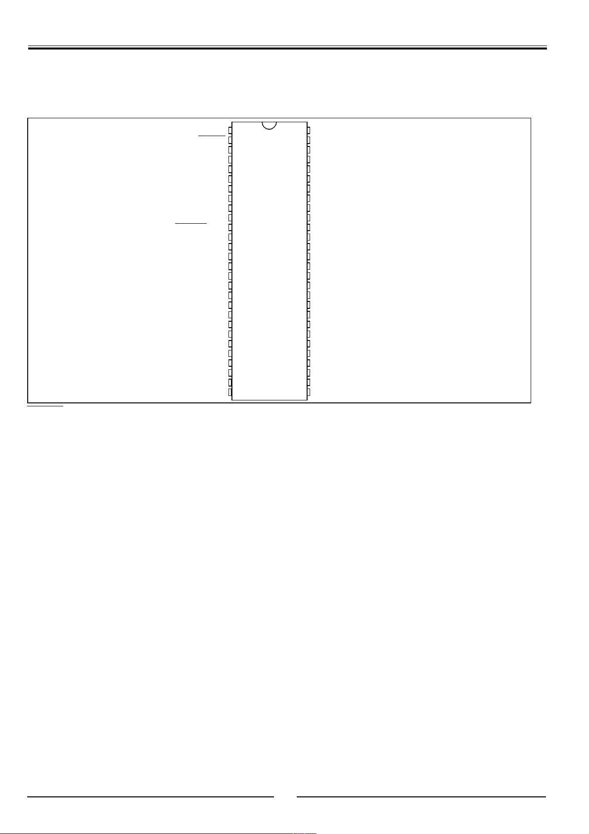
PIN DESCRIPTION (Cont’d)
Figure 3. 56-Pin Package Pin-Out
RESET
INT7/P2.0
RESET
AIN4/P0.2
CSO/RESET0
SDA1/SDI/SDO/P5.1
SCL1/SCK/INT2/P5.0
WSCF
V
/WSCR
PP
AVDD3
TEST0
MCFM
Reset (input, active low). The ST9+ is ini-
P0.7
P0.6
P0.5
P0.4
P0.3
P0.1
P0.0
/P3.7
P3.6
P3.5
P3.4
FB
V
DD
JTDO
JTCK
1
2
3
4
5
6
7
8
9
10
11
12
13
14
15
B
16
G
17
R
18
19
20
21
22
23
24
25
26
27
28
tialised by the Reset signal. Wi th the d eactivation
of RESET, program execution begins from the
Program memory location pointed to by the vector
contained in program mem ory locations 00h and
01h.
R/G/B Red/Green/Blue. Video color analog DAC
outputs.
FB Fast Blanking. Video analog DAC output.
V
Main power supply voltage (5V±10%, digital)
DD
WSCF, WSCR Analog pins for the VPS/WSS slic-
er . These pins must be tied to ground or not connected.
V
: On EPROM/OTP devices, the WSCR pin is
PP
replaced by V
pin. V
should be tied to GND in user mode.
PP
which is the programming voltage
PP
MCFM Analog pin for the displa y pixel frequency
multiplier.
OSCIN, OSCOUT Oscillator (input and output).
These pins connect a parallel-resonant crystal
(24MHz maximum), or an external source to the
on-chip clock oscillator and buffer. OSCIN is the
input of the oscillator inverter and internal clock
generator; OSCOUT is the output of the oscillator
P2.1/INT5/AIN1
56
P2.2/INT0/AIN2
55
P2.3/INT6/VS01
54
P2.4/NMI
53
P2.5/AIN3/INT4/VS02
52
OSCIN
51
OSCOUT
50
P4.7/PWM7/EXTRG/STOUT0
49
P4.6/PWM6
48
P4.5/PWM5/SDA2
47
P4.4/PWM4/SCL2
46
P4.3/PWM3/TSLU/HT
45
P4.2/PWM2
44
P4.1/PWM1
43
P4.0/PWM0
42
VSYNC
41
HSYNC/CSYNC
40
AVDD1
39
PXFM
38
37
JTRSTO
GND
36
AGND
35
CVBS1
34
CVBS2
33
JTMS
32
AVDD2
31
CVBSO
30
29
TXCF
VSYNC Vertical Sync. Vertical video synchr
tion input to OSD. Positive or negative
HSYNC/CSYNC Horizontal/Composite sync. Hori-
zontal or composite video synchronisati
OSD. Positive or negative polarity.
PXFM Analog pin for the Display Pixel
Multiplier
AVDD3 Analog V
to V
externa lly .
DD
GND Digital circuit ground.
AGND Analog circuit ground (must be ti
nally to digital GND).
CVBS1 Composite video input signal for
text slicer and sync extraction.
CVBS2 Composite video input signal for
WSS slicer. Pin AC coupled.
AVDD1, AVDD2 Analog power supplies (mus
tied externally to AVDD3).
TXCF Anal og pin for the Teletext slicer
CVBSO, JTDO, JTCK Test pins: leave float
TEST0 Test pins: must be tied to AVDD2.
JTRST0 Test pin: must be tied to GND.
inverter.
of PLL. This pin m ust be
DD
46
Page 47
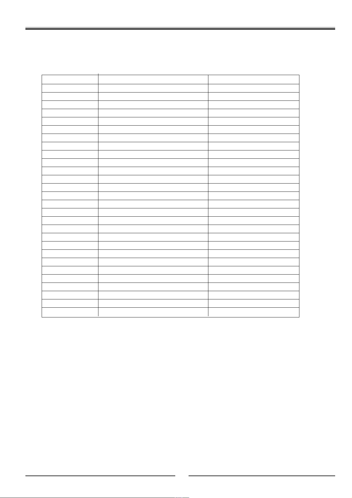
PIN ASSIGNMENT
PPiinn NNoo.. PPiinn NNaammee II//OO FFuunnccttiioonn
1 INT7/P2.0 IR INT. IN
3 P0.7 DVDDATAOUT
4 P0.6 STOP
5 P0.5 N.C.
6 P0.4 N.C.
7 P0.3 N.C.
8 AIN4 AV.STATUS
9 P0.1 N.C.
10 P0.0 N.C.
11 CSO/RESET0/P3.7 MUTE_DVD
12 P3.6 L/L'
13 P3.5 TV/DVD
14 P3.4 STDBY
28 JTCK N.C.
30 CVBSO N.C.
32 JTMS N.C.
42 P4.0/PWMO DVD_STD_BY
43 P4.1/PWM1 VOL
44 P4.2/PWM2 N.C.
45 P4.3/PWM3 DVD POWER +5V
46 P4.4/PWM4 DVD POWER +12V
47 P4.5/PWM5 N.C.
48 P4.6/PWM6 N.C.
49 P4.7/PWM7/EXTRG/STOUT N.C.
53 P2.4/NMI N.C.
54 P2.3/INT6/VS01 LED CONTROL
55 P2.2/INT0/AIN2 DVDDATAIN
56 P2.1/INT5/AIN1 KEYBOARD INPUT
PT 90 NEAT Service Manual
47
Page 48
PT 90 NEAT Service Manual
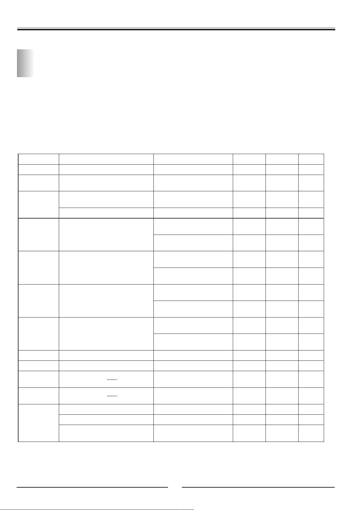
24C08 pos: IC02
Non-Volatile Memory
These I_C-compatible electrically erasable programmable memory (E_PROM) is organized as 1024 x 8 bit and operate
with a power supply of 5 V. The memory behaves as a slave device in the I_C protocol, with all memory operations synchronized by the serial clock. Read and Write operations are initiated by a START
condition, generated by the bus master. The START condition is followed by a Device Select Code and RW bit terminated
by an acknowledge bit.
DC Characteristics
= 0 to 70°C, –20 to 85°C or –40 to 85°C; VCC = 3V to 5.5V, 2.5V to 5.5V or 1.8V to 5.5V
(T
A
Symbol Parameter Test Condition Min Max Unit
I
I
I
I
I
I
I
CC
CC1
CC2
CC3
CC4
V
V
V
V
LI
LO
IL
IH
IL
IH
Input Leakage Current 0V≤ VIN≤ V
Output Leakage Current
Supply Current (ST24 series)
Supply Current (ST25 series) V
Supply Current (Standby)
(ST24 series)
Supply Current (Standby)
(ST25 series)
Supply Current (Standby)
(ST24C08R)
Supply Current (Standby)
(ST24C08R)
0V ≤ V
SDA in Hi-Z
V
= 5V, fC = 100kHz
CC
(Rise/Fall time < 10ns)
= 2.5V, fC = 100kHz 1 mA
CC
= VSS or VCC,
V
IN
V
CC
V
= VSS or VCC,
IN
= 5V, fC = 100kHz
V
CC
V
= VSS or VCC,
IN
V
CC
V
= VSS or VCC,
IN
V
= 2.5V, fC = 100kHz
CC
= VSS or VCC,
V
IN
V
CC
V
= VSS or VCC,
IN
V
= 3.6V, fC = 100kHz
CC
V
= VSS or VCC,
IN
V
CC
V
= VSS or VCC,
IN
V
= 1.8V, fC = 100kHz
CC
CC
≤ V
OUT
= 5V
= 2.5V
= 3.6V
= 1.8V
CC
Input Low Voltage (SCL, SDA) –0.3 0.3 VCCV
Input High Voltage (SCL, SDA) 0.7 VCCVCC + 1 V
Input Low Voltage
(E, PRE, MODE,
WC)
Input High Voltage
(E, PRE, MODE,
WC)
–0.3 0.5 V
V
– 0.5 VCC + 1 V
CC
±2 µA
±2 µA
2mA
100 µ A
300 µ A
5 µA
50 µA
20 µA
60 µA
10 µA
20 µA
Output Low Voltage (ST24 series) I
V
OL
Output Low Voltage (ST25 series) I
Output Low Voltage
(ST24C08R)
= 3mA, VCC = 5V 0.4 V
OL
= 2.1mA, VCC = 2.5V 0.4 V
OL
= 1mA, VCC = 1.8V 0.3 V
I
OL
48
Page 49
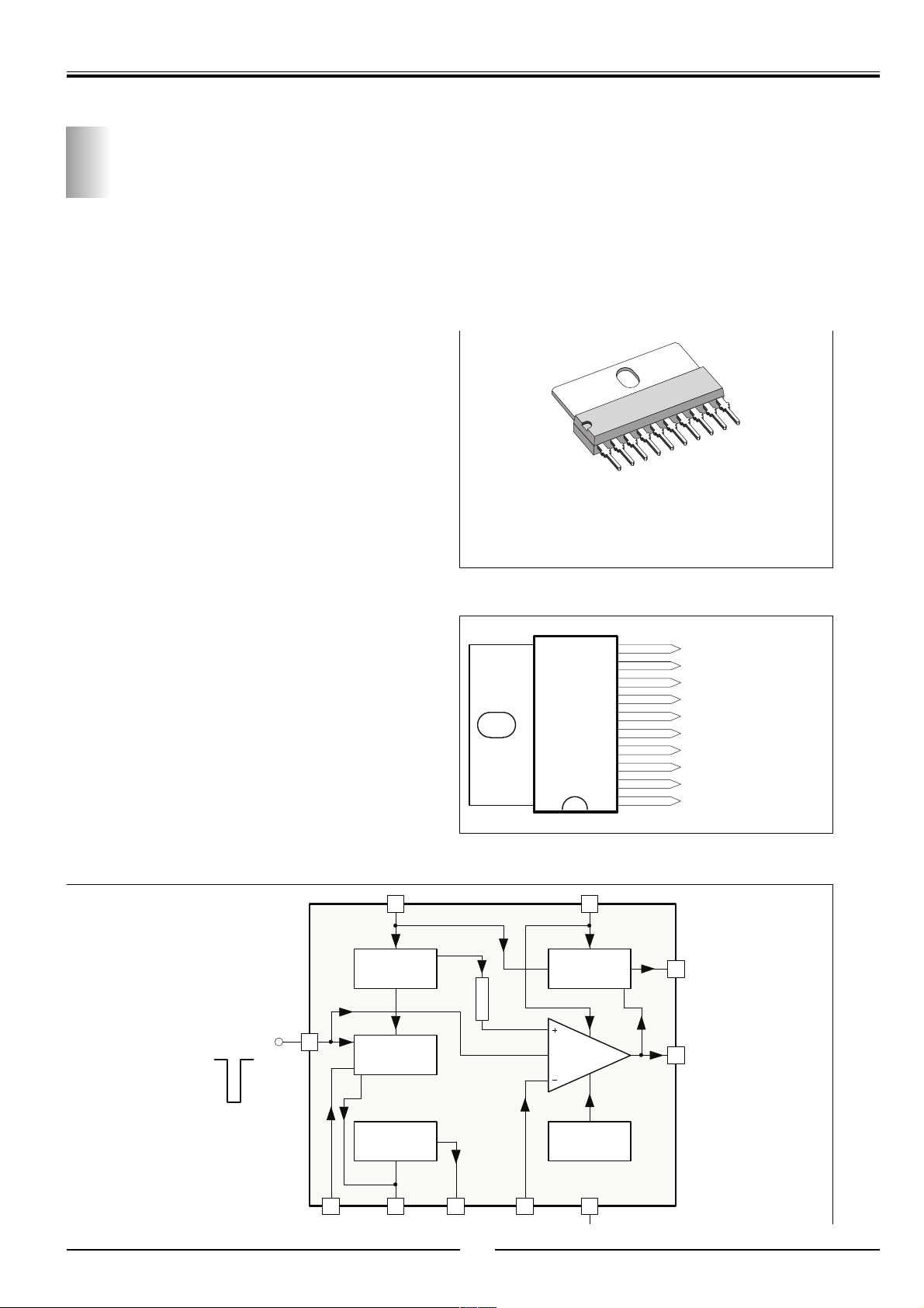
PT 90 NEAT Service Manual
TDA1771 pos: ID41
VERTICAL DEFLECTION CIRCUIT
DESCRIPTION
The TDA1771 is a monolithic integrated circuit in SIP10 package.
It is a full performance and very efficient vertical deflection circuit intended for direct drive of a TV picture tube in Color and
B & W television as well as in Monitor and Data displays.
RAMP GENERAT OR
INDEPENDENT AMPLI TUDE ADJUSTEMENT
BUFFER STAGE
POWER AMPLIFIER
FLYBACK GENERA T O R
INTERNAL REFE RENC E VOLTAGE
THERM AL PROTECTION
SIP10
(Plastic Package)
ORDER CODE : TDA1771
PIN CONNECTIONS (top view)
SCRIPTION
e TDA1771 is a monolithic i ntegrated circuit in
P10 package.
is a full performance and very efficient vertical
flection circuit intended for direct drive of a TV
cture tube in Color and B & W television as well
in Monitor and Data displays.
OCK DIAGRAM
9
VOLTAGE
REGULATOR
R3
FLYBACK
GENERATOR
10
9
8
7
6
5
4
3
2
1
2
FLYBACK GENERATOR
V
S
INVERTING INPUT
BUFFER OUTPUT
RAMP GENERATOR
GROUND
HEIGHT ADJUSTMENT
TRIGGER INPUT
OUTPUT STAGE V
POWER OUTPUT
10
S
1771-01.EPS
TRIGGER IN
3
467 85
RAMP
GENERATOR
BUFFER
STAGE
CLOCK
PULSE
POWER
AMP.
THERMAL
PROTECTION
49
1
-02.EPS
Page 50
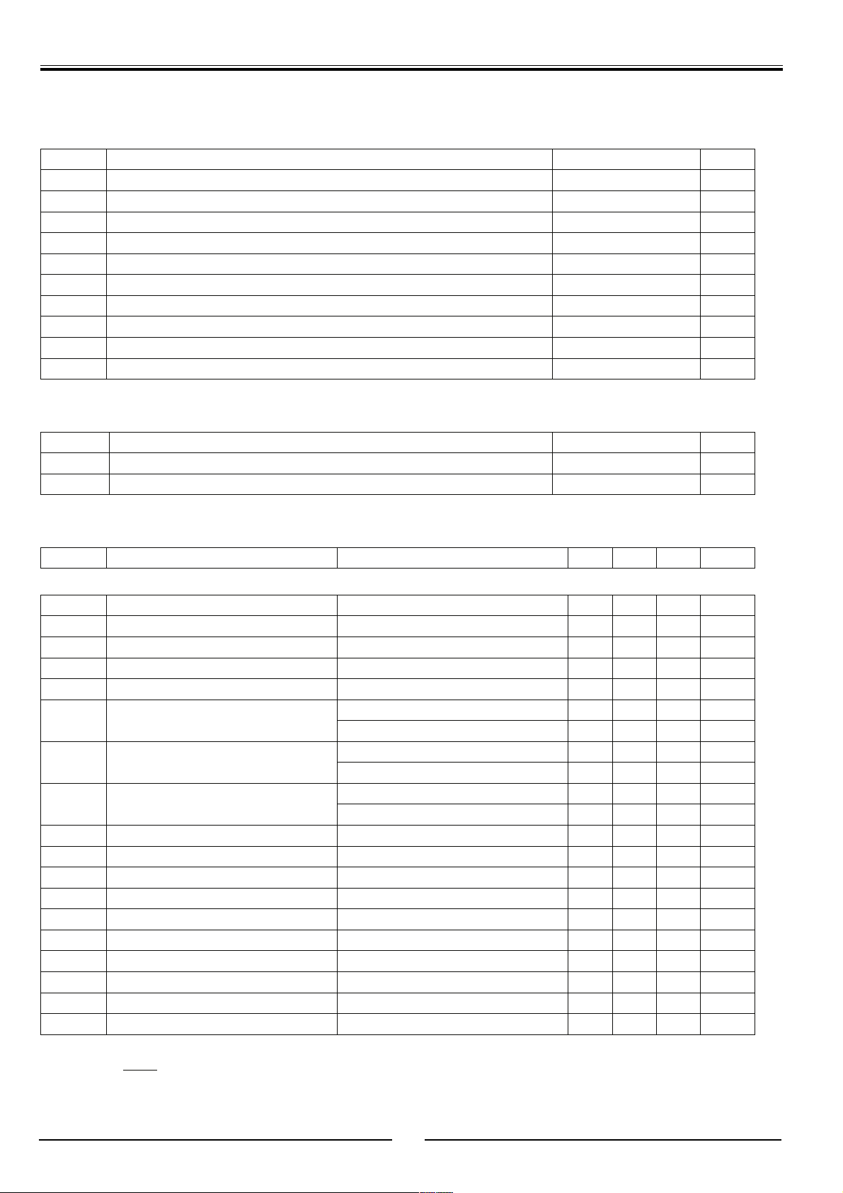
PT 90 NEAT Service Manual
V
.
ABSOLUTE MAXIMUM RATINGS
Symbol Parameter Value Unit
V
, V2Flyback Peak Voltage 65 V
V
1
V
V
I
I
I
10
I
10
P
, TJStorage and Junction Temperature – 40, + 150°C
T
S
Supply Voltage 30 V
S
Trigger Input Voltage 20 V
3
Amplifier Input Voltage GND to VSV
8
Output Peak to Peak Current (non repetitive t = 2ms) 6
0
Output Peak to Peak Current t > 10µs4A
0
Pin 10 DC Current at V
Pin 10 Peak to Peak Current @ t
Total Power Dissipation @ T
tot
< V
1
9
< 1.5ms 3 A
fly
= 60°C9W
tab
100 mA
THERMAL DATA
Symbol Parameter Value Unit
R
th (j-tab)
R
th (j-a)
Thermal Resistance Junction-tab Max. 10 °C/W
Thermal Resistance Junction-ambient Max. 70 °C/W
1771-01.TBL
1771-02.TBL
ELECTRICAL CHARACTERISTICS (T
= 25°C unless otherwise specified)
amb
Symbol Parameter Test Conditions Min. Typ. Max. Unit
DC (V
= 30V)
S
dI
dV
dV
I
2
I
9
– I
6
– I
6
6/I6
V
1
V
1L
V
1H
V
4
4/VS
4/dI 4
V
r
Pin 2 Quiescent Current I
Pin 9 Quiescent Current I
Ramp Generator Bias Current V
Ramp Generator Current V6 = 0, – I4 = 20µA 18.5 20 21.5 µA
Ramp Gener. Linearity V6 = 0 to 15V, – I
Quiescent Output Voltage R
Out Saturation Voltage to GND I
Out Saturation Voltage to VS– I1 = 0.5A 1.1 1.6 V
Reference Voltage – I
Reference Voltage Drift Versus VSVS = 10V to 30V 1 2 mV/V
Reference Voltage Drift Versus I4I4 = 10µA to 30µA 1.5 2 mV/µA
Internal Ref. Voltage 4.26 4.40 4.54
= 0, I10 = 0 16 36 mA
1
= 0, I10 = 0 15 30 mA
1
= 0 0.5 µA
6
= 20µA0.21%
4
= 30kΩ, Rb = 10kΩ, VS = 30V 17.0 17.8 18.6 V
a
= 6.8kΩ, Rb = 10kΩ, VS = 15V 7.2 7.5 7.8 V
R
a
= 0.5A 0.5 1 V
1
= 1.2A 1 1.4 V
I
1
= 1.2A 1.6 2.2 V
– I
1
= 20µA 6.3 6.6 6.9 V
4
Gv Ouput Stage Open Loop Gain f = 100Hz 60 dB
V
V
fs
V
10
V
3
I
3
t
3
Notes : 1. The trigger input circuit can accept, with a metal option, positive and negative going input pulses
2. th=
Saturation Voltage – I
9 – 10
Pin 10 Scanning Voltage I
Trigger Input Threshold (see note 1) 2.6 3.0 3.4
Trigger Input Bias Current V
Trigger Input Width (see note 2) 20 60 thµS
t
1.2⋅
S
where tS is the vertical period and V
V
PP
= 1.2A 1.5 2.5 V
10
= 20mA 1.7 3 V
10
= V3 – 0.2V 30 µA
IN
is ramp amplitude at Pin 6
PP
1171-03.TBL
50
Page 51
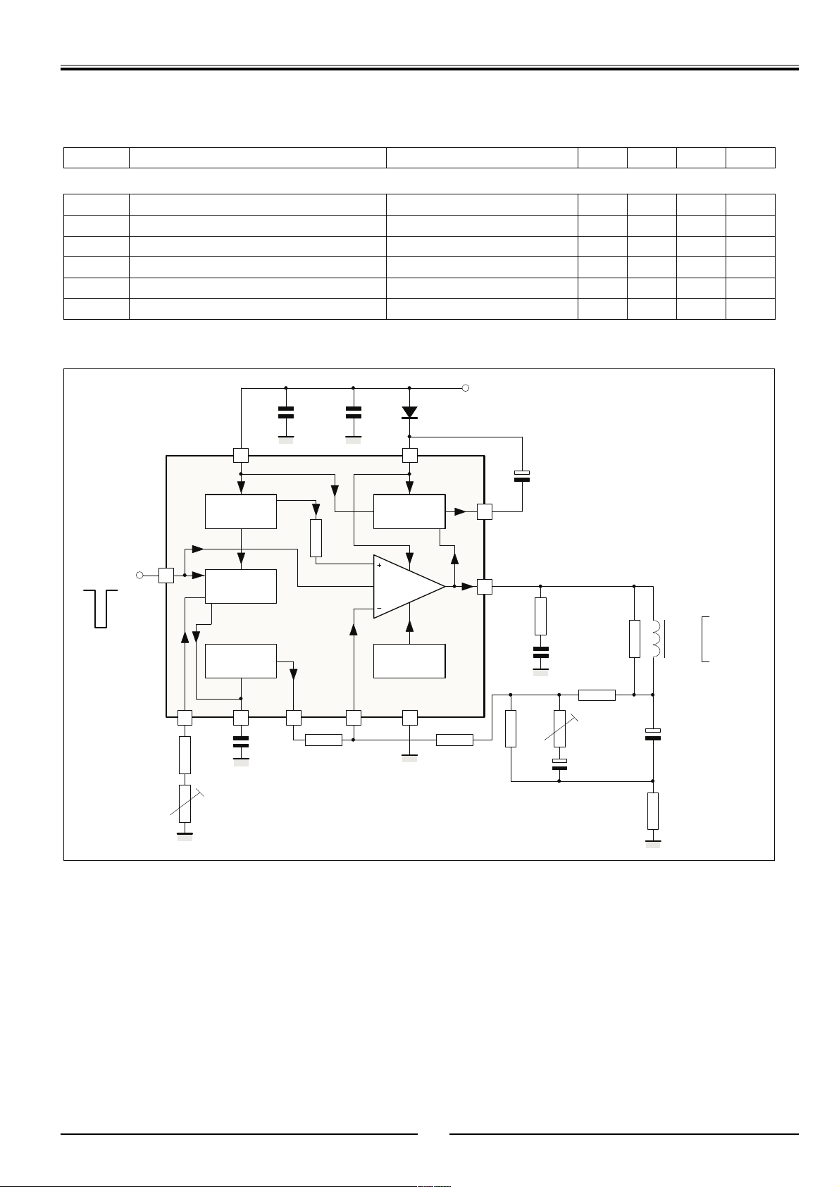
PT 90 NEAT Service Manual
V
V
ELECTRICAL CHARACTERISTICS (T
= 25°C unless otherwise specified) (continued)
amb
Symbol Parameter Test Conditions Min. Typ. Max. Unit
DC (V
= 24V)
S
V
S
I
1
I
S
V
1
V
7
T
JS
Operating Supply Voltage Range 10 30
Peak-to-peak Operating Current Range 0.4 2.5
Supply Current IY = 2.4A
Flyback Voltage IY = 2.4A
pp
pp
315 mA
51 V
Sawtooh Pedestall Voltage 1.85
Junction Temp. for Thermal Shutdown 145 °C
APPLICATION CIRCUIT
+V
S
0.1µF470
9
VOLTAGE
REGULATOR
R3
µ
F
GENERATOR
2
FLYBACK
1N4001
100µF
35V
10
1771-04.TBL
TRIGGER IN
3
467 85
180k
Ω
220k
Ω
RAMP
GENERATOR
BUFFER
STAGE
47nF
CLOCK
PULSE
POWER
AMP.
PROTECTION
THERMAL
1
1.2k
Ω
2.2Ω
0.22µF
1k
22µF
2.4k
Ω
330
Ω
Ω
1.2
YOKE
1500µF
Ω
Ω
Ry = 9.6
Ly = 24.6mH
Iy = 1.2App
1771-03.EPS
51
Page 52
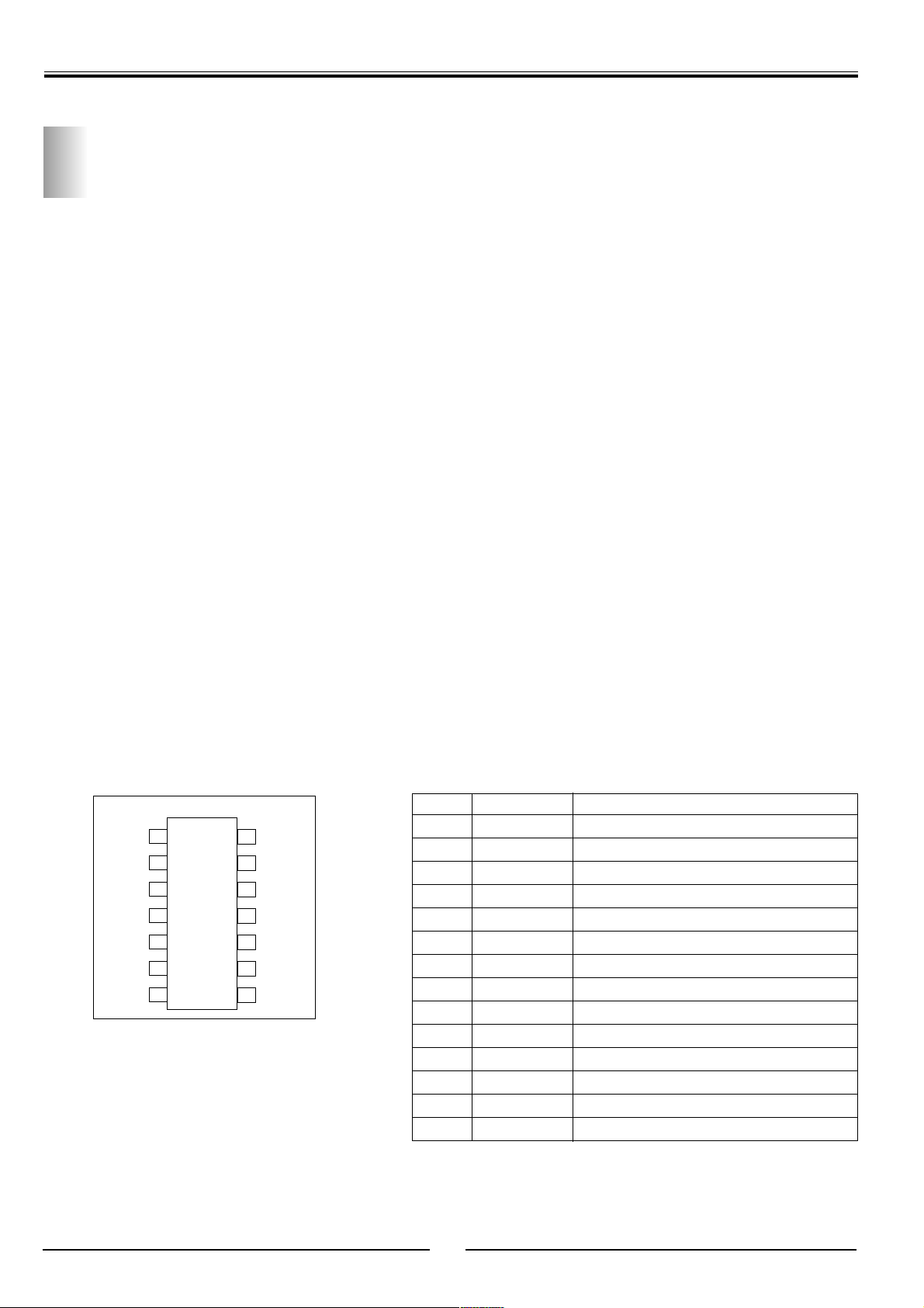
PT 90 NEAT Service Manual
TDA 16846 pos: IP01
Controller for Switch Mode Power Supplies Supporting Low Power
Standby and Power Factor Correction
Features
•
Line Current Consumption with PFC
•
Low Power Consumption
•
Stable and Adjustable Standby Frequency
•
Very Low Start-up Current
•
Soft-Start for Quiet Start-up
•
Free usable Fault Comparators
•
Synchronization and Fixed Frequency Facility
•
Over- and Undervoltage Lockout
•
Switch Off at Mains Undervoltage
•
Temporary high power circuit (only TDA 16847)
•
Mains Voltage Dependent Fold Back Point Correction
•
Continuous Frequency Reduction with Decreasing
Load
•
Adjustable and Voltage Dependent Ringing Suppression Time
Description
The TDA 16846 is optimised to control free running or
fixed frequency flyback converters with or without Power
Factor Correction (Current Pump). To provide low power
consumption at light loads, this device reduces the
switching frequency continuously with load, towards an
adjustable minimum (e. g. 20 kHz in standby mode).
Additionally, the start up current is very low. To avoid
switching stresses of the power devices, the power transistor is always switched on at minimum voltage. A special circuit is implemented to avoid jitter. The device has
several protection functions: V CC over- and undervoltage, mains undervoltage, current limiting and 2 free
usable fault comparators. Regulation can be done by
using the internal error amplifier or an opto coupler feedback (additional input). The output driver is ideally suited
for driving a power MOSFET, but it can also be used for
a bipolar transistor. Fixed frequency and synchronized
operation are also possible. The TDA 16846 is suited for
TV-, VCR- sets and SAT receivers. It also can be good
used in PC monitors. The TDA 16847 is identical with
TDA 16846 but has an additional power measurement
output (pin 8) which can be used for a Temporary High
Power Circuit.
Pin Configuration (top view)
U
DTC
PCS
RZI
SRC
OCI
FC2
SYN
1
2
3
4
5
6
7
14
13
12
11
10
9
8
VCC
OUT
GND
PVC
FC1
REF
N.C./PMO
Pin Definitions and Functions
Pin Symbol Function
1 OTC Off Time Circuit
2 PCS Primary Current Simulation
3 RZI Regulation and Zero Crossing Input
4 SRC Soft-Start and Regulation Capacitor
5 OCI Opto Coupler Input
6 FC2 Fault Comparator 2
7 SYN Synchronization Input
8 N.C./PMO Not Connected (TDA16846)
9 REF Reference Voltage and Current
10 FC1 Fault Comparator 1
11 PVC Primary Voltage Check
12 GND Ground
13 OUT Output
14 VCC Supply Voltage
52
Page 53
Short Description of the Pin Functions
Pin Functions
1 A parallel RC-circuit between this pin and ground determines the ringing suppression time
and the standby-frequency.
2 A capacitor between this pin and ground and a resistor between this pin and the positive
terminal of the primary elcap quantifies the max. possible output power of the SMPS.
3 This is the input of the error amplifier and the zero crossing input. The output of a voltage
divider between the control winding and ground is connected to this input. If the pulses at
pin 3 exceed a 5 V threshold, the control voltage at pin 4 is lowered.
4 This is the pin for the control voltage. A capacitor has to be connected between this pin
and ground. The value of this capacitor determines the duration of the softstart and the
speed of the control.
PT 90 NEAT Service Manual
5 If an opto coupler for the control is used, it's output has to be connected between this pin
and ground. The voltage divider at pin 3 has then to be changed, so that the pulses at pin
3 are below 5 V.
6 Fault comparator 2: If a voltage > 1.2 V is applied to this pin, the SMPS stops.
7 If fixed frequency mode is wanted, a parallel RC circuit has to be connected between this
pin and ground. The RC-value determines the frequency. If synchronized mode is wanted,
sync pulses have to be fed into this pin.
8 Not connected (TDA16846). / This is the power measurement output of the Temporary
High Power Circuit. A capacitor and a RC-circuit has to be connected between this pin
and ground.
9 Output for reference voltage (5 V). With a resistor between this pin and ground the fault
comparator 2 (pin 6) is enabled.
10 Fault comparator i: If a voltage > 1 V is applied to this pin, the SMPS stops.
11 This is the input of the primary voltage check. The voltage at the anode of the primary
elcap has to be fed to this pin via a voltage divider. If the voltage of this pin falls below
1 V, the SMPS is switched off. A second function of this pin is the primary voltage dependent fold back point correction (only active in free running mode).
12 Common ground.
13 Output signal. This pin has to be connected across a serial resistor with the gate of the
power transistor.
14 Connection for supply voltage and startup capacitor. After startup the supply voltage is
produced by the control winding of the transformer and rectified by an external diode.
53
Page 54
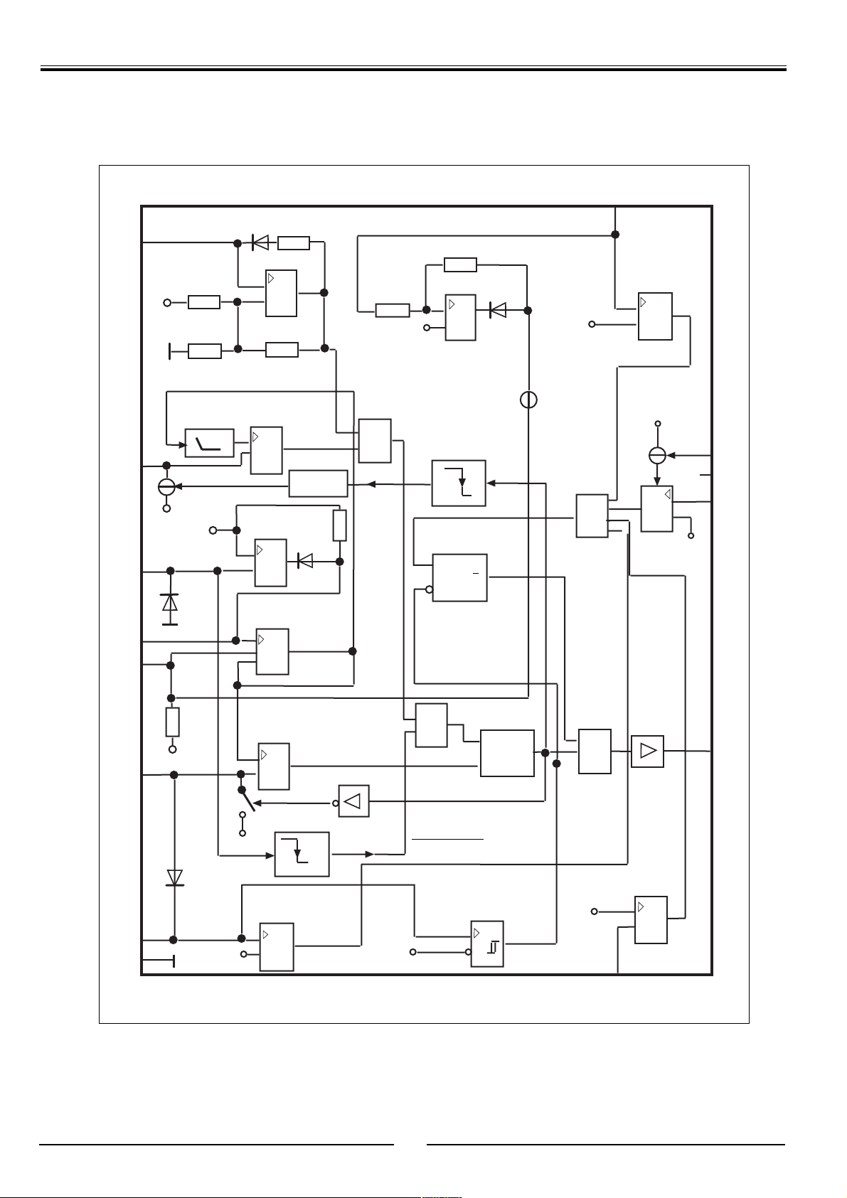
PT 90 NEAT Service Manual
TDA16846 Block Diagrams
PVC
SYN
OTC
RZI
SRC
OCI
5V
1
3
4
5
3.5V
CS1
D
R
30kΩ
R
75kΩ
Limit
5V
3
D
4
7
8
Control Voltage
Off Time
Comparator
5V
Amplifier
Control Voltage
KSY
∞
+
R
15kΩ
∞
+
-
Eror
∞
+
-
Buffer for
∞
+
+
-
R
4
3
RSTC/RSTF
R
D
2
G4
11
Primary
Voltage
Check
∞
+
V
CC
9
REF
8
N.C.
1
∞
FC2
6
+
–
FC2
1.2V
Fold Back Point Correction
R6x1/3
R
6
1.5V
G1
1
2
PVA
-
+
ED2
Error-
Flipflop
S
R
D5
∞
1V
–
3.5V
+
Q
R
1
20kΩ
5V
2
PCS
D1
Startup
Diode
14
V
CC
12
GND
1)
The input with the lower voltage becomes operative
16V
1.5V
On Time
Comparator
∞
+
ED1
<25mV
Overvoltage
Comparator
∞
+
-
&
S
G2
I
1
Zero Crossing
Signal
Supply Voltage
Comparator
15.8V
+
-
Q
R
∞
G3
1V
Output
Driver
&
FC1
∞
13
OUT
-
+
10
54
Page 55
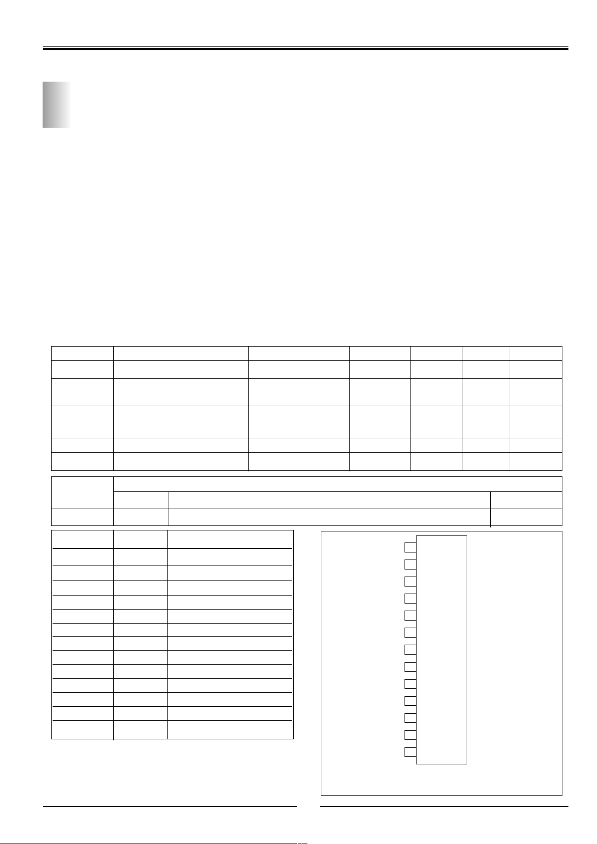
PT 90 NEAT Service Manual
TDA7057AQ
2 x5 W stereo BTL Audio Output Amplifier with DC Volume Control
FEATURES
• DC volume control
• Few external components
• Mute mode
• Thermal protection
• Short-circuit proof
• No switch-on and switch-off clicks
• Good overall stability
• Low power consumption
• Low HF radiation
• ESD protected on all pins.
GENERAL DESCRIPTION
The TDA7057AQ is astereo BTL output amplifier with DC
volume control. The device is designed for use in TV and
monitors, but are also suitable for battery-fed portable
recorders and radios.
Missing Current Limiter (MCL)
A MCL protection circuit is built-in. The MCL circuit is
activated when the difference in current between the
output terminal of each amplifier exceeds 100 mA (typical
300 mA). This level of 100 mA allows for headphone
applications (single-ended).
QUICK REFERENCE DATA
SYMBOL PARAMETER CONDITIONS MIN. TYP. MAX. UNIT
V
P
P
out
G
v
G
C
I
q(tot)
THD total harmonic current P
supply voltage 4.5 – 18 V
output power Vp = 12 V; RL= 16 Ω 3.0 3.5 – W
= 12 V; RL= 8Ω – 5.3 – W
V
p
voltage gain 39.5 40.5 41.5 dB
gain control 68.0 73.5 – dB
total quiescent current Vp = 12 V; RL= ∞ – 22 25 mA
=0.5w w – 0.3 1 %
out
TYPE PACKAGE
NUMBER NAME DESCRIPTION VERSION
TDA7057AQ DBS13P Plastic DIL-bent-SIL power package; 13 leads (lead length 12 mm) SOT141-6
SYMBOL PIN DESCRIPTION
VC1 1 DC volume contol 1
n.c. 2 not connected
V
I (1)
V
P
V
I (2)
3 voltage input 1
4 positive supply voltage
5 voltage input 2
SGND 6 signal ground
VC2 7 DC volume contol 2
OUT2+ 8 positeve output 2
PGND2 9 power ground 2
OUT2- 10 negative output 2
OUT1- 11 negative output 1
PGND1 12 powwer ground 1
OUT1+ 13 positive output 1
vc1
n.c.
V
I(1)
V
SGND
VC2
OUT2
PGND2
OUT2–
OUT1-
PGND1
OUT1+
V
P
I(2)
1
2
3
4
5
6
7
8
9
10
11
12
13
U
TDA7057AQ
55
Pin Configuration
Page 56
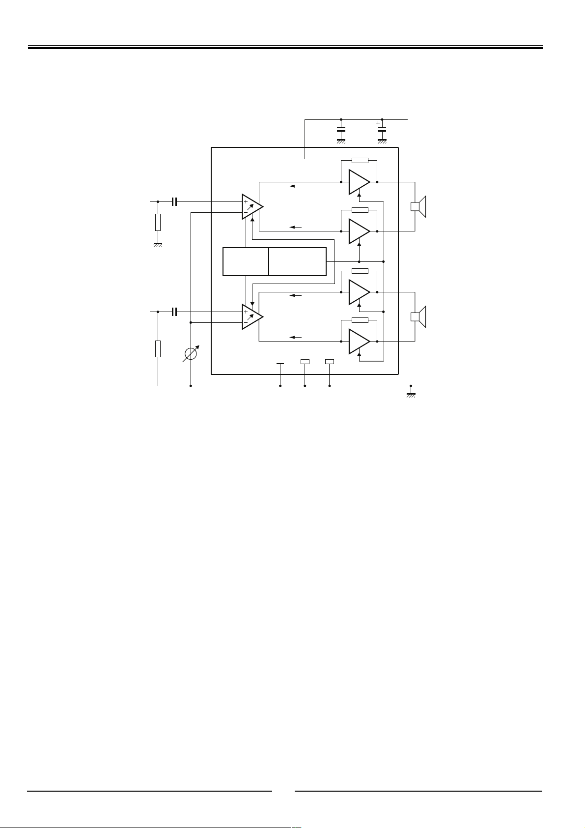
PT 90 NEAT Service Manual
handbook, full pagewidth
input 1
Rs = 5 kΩ
input 2
Rs = 5 kΩ
470 nF
470 nF
DC-
volume
TDA7053AQ
3
1
STABILIZER
5
7
I+ 1
I− 1
TEMPERATURE
MCL
PROTECTION
I− 1
I+ 1
signal
ground
4
9 126
power
ground
(1)
100 nF
VP = 12 V
220µF
13
(2)
11
10
(2)
8
(1) This capacitor can be omitted if the 220µF electrolytic capacitor is connected close to pin 5.
(2) RL=16Ω.
FUNCTIONAL DESCRIPTION
The TDA7057AQ is a stereo output amplifiers with two
DC volume control stages. The device is designed for TV
and monitors, but also suitable for battery-fed portable recorders and radios.
In conventional DC volume control circuits the control or
input stage is AC coupled to the output stage via external
capacitors to keep the offset voltage low.
In the TDA7057AQ the two DC volume control stages are
integrated into the input stages so that no coupling capacitors are required and a low offset voltage is still maintained. The minimum supply voltage also remains low.
The BTL principle offers the following advantages:
• Lower peak value of the supply current
• The frequency of the ripple on the supply voltage is twice the signal frequency.
Consequently, a reduced power supply with smaller capa
citors can be used which results in cost reductions.
For portable applications there is a trend to decrease the
supply voltage, resulting in a reduction of output power at
conventional output stages. Using the BTL principle increases the output power.
The maximum gain of the amplifier is fixed at 40.5 dB.
The DC volume control stages have a logarithmic control
characteristic. Therefore, the total gain can be controlled
from +40.5 dB to -33 dB. If the DC volume control voltage
falls below 0.4 V, the device will switch to the mute mode.
The amplifier is short-circuit protected to ground, Vp and
across the load. A thermal protection circuit is also implemented. If the crystal temperature rises above 150 oC the
gain will be reduced, thereby reducing the output power.
Special attention is given to switch-on and switch-off
clicks, low HF radiation and a good overall stability.
56
Page 57
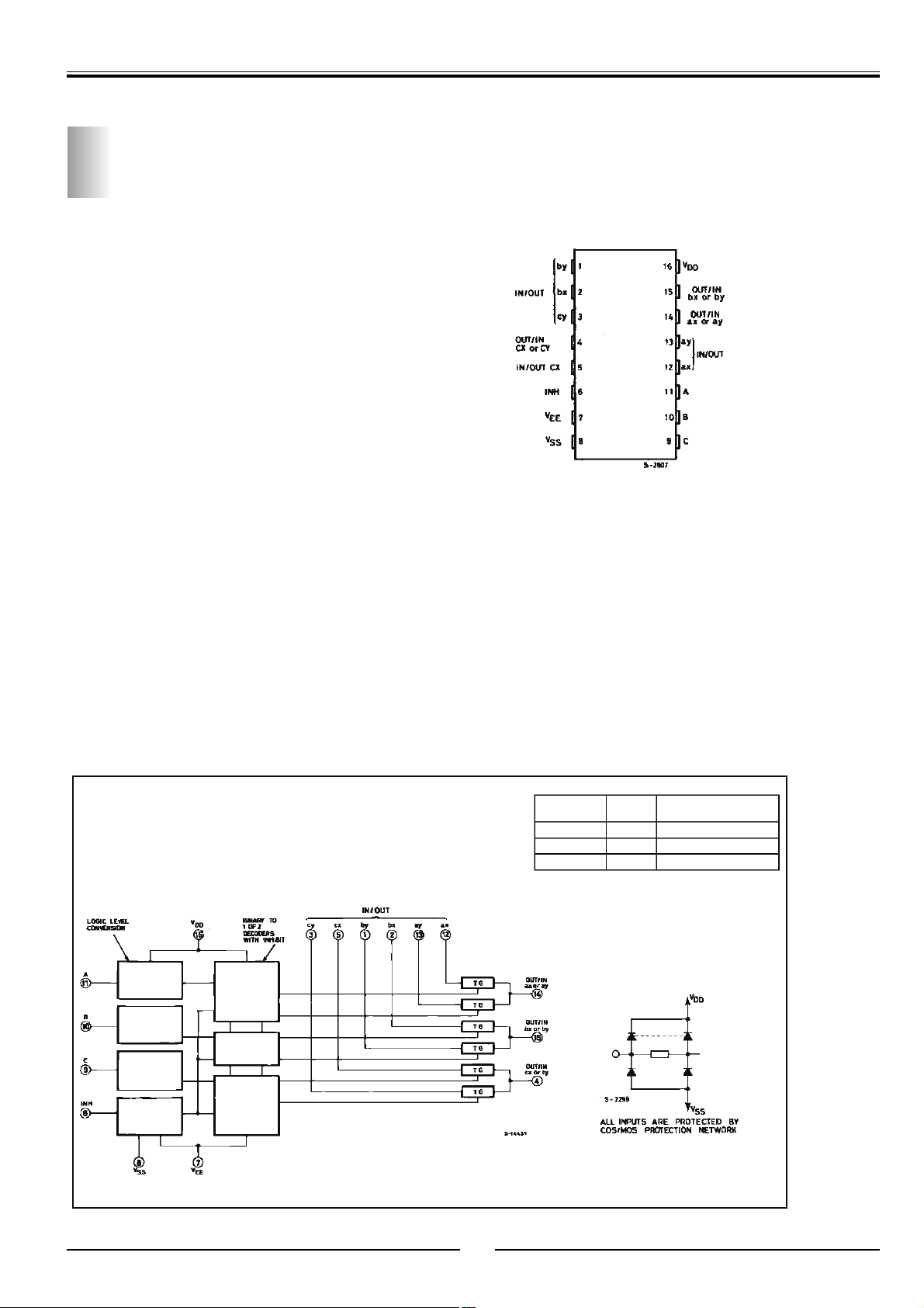
74HC4053B pos:IA03
h
p
Analog Multiplexer/Demultiplexer
4053B
.
QUIESCE NT CURREN T SPECIFIED TO 20V
FOR HCC DEVICE
.LOW ”ON” RESISTANCE : 125Ω (typ.) OVER
15V p.p. SIGNAL-INPUT RANGE FOR V
VEE= 15V
DD
-
EY
(Plastic Package)F(CeramicFritSeal Package)
.HIGH ”OFF” RESISTANCE : CHANNEL LEAK-
AGE ± 100pA (typ.) VDD– VEE= 18V
.
BINARY ADDRESS DECODING ON CHIP
.
VERY LOW QUIESCENT POWER DISSIPATION UNDER ALL DIGITAL CONTROL INPUT
AND SUPPLY CONDITIONS : 0.2 µW (typ.),
VDD– VSS=VDD– VEE= 10V
.
MATCHED SWITCH CHARACTERISTICS :
R
=5Ω (typ.)for VDD– VEE= 15V
ON
M1
(Micro Package)C1(Plastic Chip Carrier)
ORDER CODES :
HCC40XXBF HCF40XXBM1
HCF40XXBEY HCF40XXBC1
.WIDE RANGEOF DIGITALAND ANALOG SIG-
NAL LEVELS : DIGITAL3 TO 20V,ANALOG TO
20V p.p.
.5V, 10V,AND 15V PARAMETRIC RATINGS
.INPUT CURRENT OF 100mA AT 18V AND
25ϒC FOR HCC DEVICE
.
100% TESTEDFOR QUIESCENTCURRENT
.MEETS ALLREQUIREMENTSOFJEDECTEN-
TATIVE STANDARD N
SPECIFICATIONS FOR DESCRIPTION OF ”B”
SERIES CMOS DEVICES”
o
13A, ”STANDARD
DESCRIPTION
TheHCC 4051B, 4052B and4053B (extendedtem-
perature range) andHCF4051B, 4052B and4053B
(intermediate temperature range) are monolit
tegrated circuits, available in 16-lead dua
plastic or ceramic package and plastic micro
age. HCC/HCF4051B, HCC/HCF4052B, and
HCC/HCF4053B analog multiplexers/demult
plexers are digitally controlled analog switc
ing low ON impedance and very low OFF leakage
PT 90 NEAT Service Manual
FUNCTIONAL DIAGRAMS AND TRUTH TABLES (continued)
4053
Inh ibit
0 0 ax or bx or cx
0 1 ay or by or cy
1 X None
X=Don’t care.
AorB
or C
57
Page 58

PT 90 NEAT Service Manual
LM317 pos: IP02
1.2V TO 37V Voltage Regulator
GENERAL DESCRIPTION
The LM117 series of adjustable 3-terminal positive voltage regulators is capable of supplying in excess of 1.5A
over a 1.2V to 37V output range. They are exceptionally
easy to use and require only two external resistors to set
the output voltage. Further, both line and load regulation are better than standard fixed regulators. Also, the
LM117 is packaged in standard transistor packages
which are easily mounted and handled.
In addition to higher performance than fixed regulators,
the LM117 series offers full overload protection available only in IC’s. Included on the chip are current limit,
thermal overload protection and safe area protection. All
overload protection circuitry remains fully functional
even if the adjustment termi-nal is disconnected.
Normally, no capacitors are needed unless the device is
situ-ated more than 6 inches from the input filter capacitors in which case an input bypass is needed. An optional output capacitor can be added to improve transient
response. The adjustment terminal can be bypassed to
achieve very high ripple rejection ratios which are difficult to achieve with stan-dard 3-terminal regulators.
Besides replacing fixed regulators, the LM117 is useful
in a wide variety of other applications. Since the regulator is “floating” and sees only the input-to-output differential volt- age, supplies of several hundred volts can
be regulated as long as the maximum input to output differential is not ex-ceeded, i.e., avoid short-circuiting the
output. Also, it makes an especially simple adjustable
switching regulator, a programmable output regulator,
or by connecting a fixed resistor between the adjustment pin and output, the LM117 can be used as a precision current regulator. Sup-plies with electronic shutdown can be achieved by clamping the adjustment terminal to ground which programs the out-put to 1.2V
where most loads draw little current. For applications requiring greater output current, see LM150 series (3A)
and LM138 series (5A) data sheets. For the negative
complement, see LM137 series data sheet.
FEATURES
l Guaranteed 1% output voltage tolerance (LM317A)
l Guaranteed max. 0.01%/V line regulation (LM317A)
l Guaranteed max. 0.3% load regulation (LM117)
l Guaranteed 1.5A output current
l Adjustable output down to 1.2V
l Current limit constant with temperature
l P + Product Enhancement tested
l 80 dB ripple rejection
l Output is short-circuit protected
58
Page 59
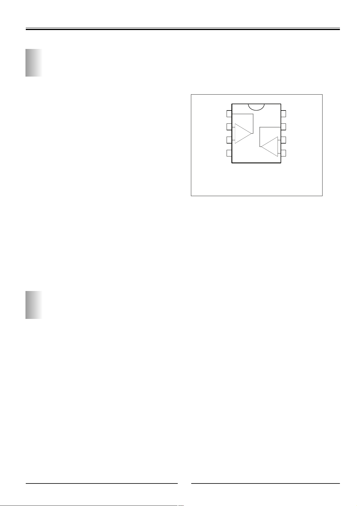
PT 90 NEAT Service Manual
LM358 pos: I060
Dual Operational Amplifier
FEATURES
• INTERNALLY FREQUENCY COMPENSATED
• LARGE DC VOLTAGE GAIN : 100dB
• WIDE BANDWIDTH (unity gain) : 1.1MHz (temperature
compen sated)
• VERY LOW SUPPLY CURRENT/OP (500mA) –ESSEN-
TIALLY INDEPENDENT OF SUPPLY VOLTAGE
• LOW INPUT BIAS CURRENT : 20nA (temperature com-
pensated)
• LOW INPUT OFFSET VOLTAGE : 2mV
• LOW INPUT OFFSET CURRENT : 2nA
• INPUT COMMON-MODE VOLTAGE RANGE INCLUDES
GROUND
• DIFFERENTIAL INPUT VOLTAGE RANGE EQUAL TO
THE POWER SUPPLY VOLTAGE
• LARGE OUTPUT VOLTAGE SWING 0V TO (VCC –
1.5V)
DESCRIPTION
These circuits consist of two independent, high gain, internally frequency compensated which were designed specifically to operate from a single power supply over a wide
range of voltages. The low power supply drain is independent of the magnitude of the power supply voltage. Application areas include transducer amplifiers, dc gain blocks
PIN CONNECTIONS
1
2
-
+
3
1 - Output 1
2 - Invertin g inp ut 1
3 - Non-inver ti ng input 1
-
4 - V
CC
and all the conventional op-amp circuits, which now can be
more easily implemented in single power supply systems.
For example, these circuits can be directly supplied with
the standard + 5V, which is used in logic systems and will
easily, provide the required interface electronics without
requiring any additional power supply. In the linear mode
the input common-mode voltage range includes ground
and the output voltage can also swing to ground, even
5 - Non-inverting input 2
6 - Inverting input 2
7 - Ouput 2
+
8 - V
CC
LM7805 pos: IP03
3-Terminal 1A Positive Voltage Regulator
Features
•
Output Current up to 1A
•
Output Voltage of 5,6,8,9,10,12,15,18,24 V
•
Thermal Overload Protection
•
Short Circuit Protection
•
Output Transistor Safe Operating Area Protection
Description
The MC78XX/LM78XX/MC78XXA series of three terminal positive regulators are available in the TO-220/DPAK package and with several fixed output voltages,
making them useful in a wide range of applications.
Each type employs internal current limiting, thermal
shutdown and safe operating are protection, making it
essentially indestructible. If adequate heat sinking is
provided, they can deliver over 1 A output current.
Although designed primarily as fixed voltage regulators,
these devices can be used with external components to
obtain adjustable voltages and currents.
59
Page 60

PT 90 NEAT Service Manual
DESCRIPTION OF INTEGRATED CIRCUITS
ES6018
DVD PROCESSOR SOLUTION
-DVD PART-
DESCRIPTION
Built on ESS’s proprietary and flexible Programmable Multimedia Processor architecture, the Vibratto TM series of
DVD processors combine audio/video stream data processing, system control and housekeeping functions, video postprocessing, and display format encoding, enabling various
DVD-based multimedia electronics to be built with minimal
external components. The Vibratto series includes new features for DVD-Audio support, progressive scan video output, and built-in TV encoder and video DACs.
All of the Vibratto DVD processors each include two parallel
processing units, a RISC processor, a vector engine, and
supplemental hardware resources for implementing specialized encoding and decoding tasks in the device architectures. All of these resources are interconnected with two
separate data buses, each with its own DMA unit and interface to external memory. The processing units enable
simultaneous parallel execution of system commands and
data processing.
Both the RISC processor and vector engine are independently programmable. Each has its own on-chip cache
memory. The RISC processor and its associated hardware
units perform bit stream parsing, control audio data output,
transfer video and audio data to the vector engine and service system control and housekeeping functions. The vector
engine and associated hardware units perform audio and
video microcode processing required by A/V standards such
as Dolby Digital TM, DTS TM, MPEG and JPEG. These
processing tasks include audio DSP, video motion compensation and estimation, loop filtering, discrete cosine transforms (DCT) and inverse DCT, quantization and inverse
quantization.
The Vibratto DVD processors support both JPEG/MP3
audio playback and the Kodak PictureCD JPEG display format. These new features allow Picture CDs created with
images and voiceovers from digital cameras to be enjoyed
in a DVD player or Home Theater System. All of the Vibratto DVD processors support both parallel and serial DVD
loader interfaces for system MPEG A/V data stream input,
industry standard-I 2 S bus for audio data input and output,
direct system EPROM and SDRAM access for high-speed
command fetching and audio/video data buffering and processing. The Vibratto DVD processors are available in 208pin Plastic Quad Flat Pack (PQFP) device packages.
FEATURES
• Dedicated core and I/O power supplies for low-power
operation; integrated 32-bit RISC processor for system
host, eliminating requirements of an external host CPU
• Supports DVD-Video, DVD-Audio, VideoCD 1.1, 2.0, and
3.0, Super VideoCD (SVCD), CD-DA, MP3, and Kodak
Picture-CD
• Supports parallel and serial interfaces to ATAPI, Compact
Flash, DCI, IDE and UDF DVD loaders
• Direct interface of 8- or 16-bit SDRAM of up to 128-Mb
capacity at a variety of speed grades
• Direct interface of up to 4 banks of 8- or 16-bit EPROM or
Flash EPROM; automatic firmware updating of Flash
EPROM through DVD loader
Video
• Built-in NTSC/PAL encoder includes field-adaptive de
interlacing for progressive scan video output for clearer
and more stable display (ES6028 and ES6038 Only)
• Macrovision 7.1 and Macrovision AGC 1.03 compliant
video outputs for 480-pixel progressive scan and for
NTSC/PAL interlaced video
• Four built-in 10-bit Video DACs provide simultaneous
video outputs of composite and S-video, or composite and
YUV; supports selectable 8-bit CCIR 601 4:2:2 YUV outputs
• 8-bit On-Screen Display (OSD) controller with 3-bit blending provides display with 256 colors in 8 degrees of transparency
• On-chip Subpicture Unit (SPU) decoder supports karaoke
lyric, subtitles, and EIA-608 compliant Line 21 Captioning
• Video error concealment, motion zoom and pan and
NTSC to PAL and PAL to NTSC conversion supported
Audio
• Dolby Digital (AC-3), DVD-Audio, Pro Logic, DTS, MPEG1 layer 2 and 3 Audio (MP3), and High-Definition Compat-
ible Digital.... (HDCD) decoding
• On-chip Dolby Digital (AC-3) and DTS 5.1 channel decoding and output (ES6018/28/38 Only)
• Dolby Digital and DTS S/PDIF digital audio output.
• Dolby Digital Class A, DTS, and HDCD certified
• Meridian Lossless Packing.... (MLP) decoding and Linear
PCM for DVD-Audio (ES6038 Only)
60
Page 61
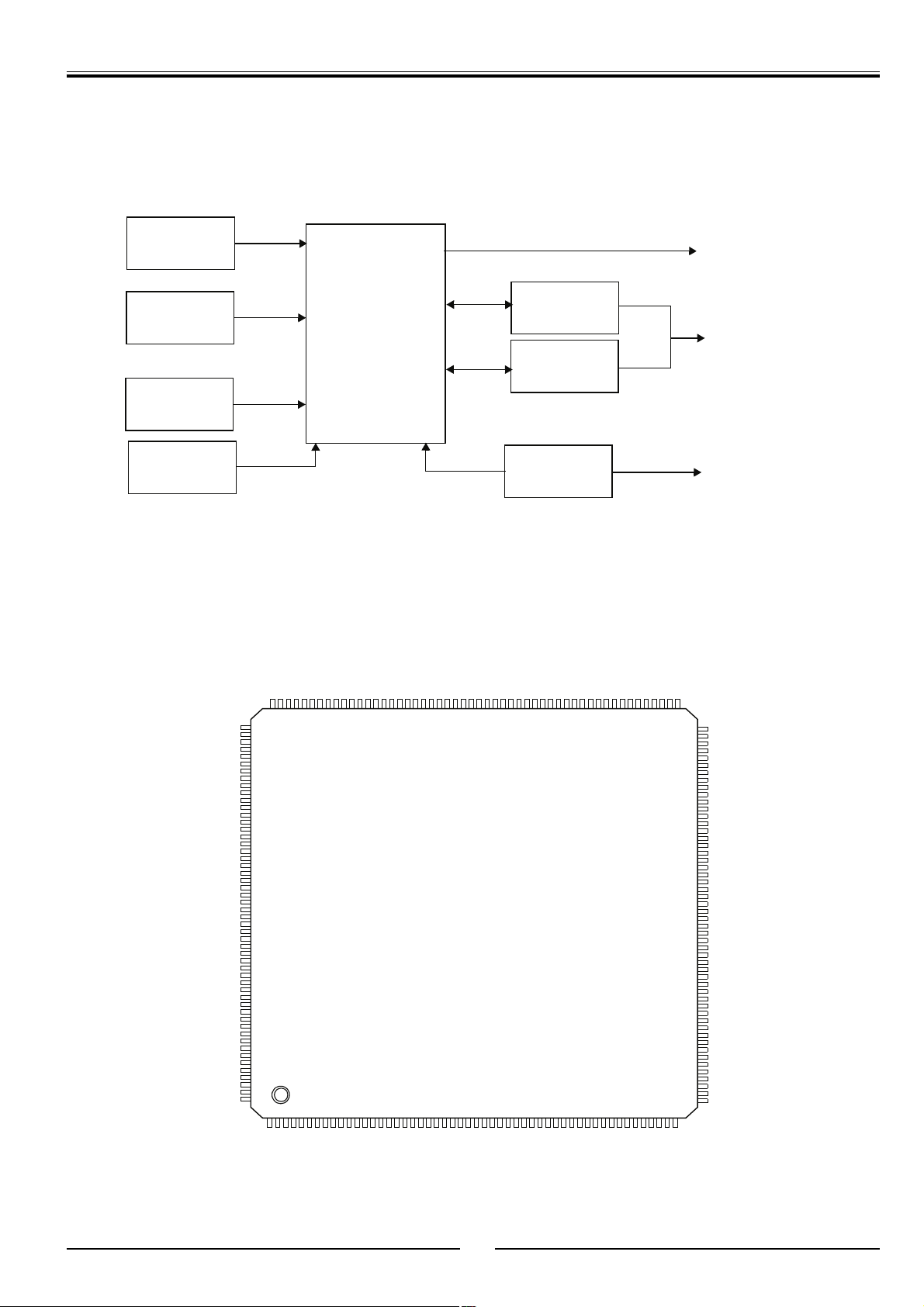
SYSTEM BLOCK DIAGRAM
PT 90 NEAT Service Manual
ROM/Flash
8 MB
SDRAM
EEPROM
DVD drive
ATAP I
Compact Flash
DCI
TVM
UDE
VSTEM
HCS3FX#/AUX3[6]
HCS1FX#/AUX3[7]
HIOCS16#/CAMCLK/AUX3[4]
HA1/AUX4[3]
VSS
HA0/AUX4[2]
Vibratto
VSS
HIORDY/AUX3[3]
HIRQ/DCI_ERR#/AUX4[7]
HRST#/AUX3[5]
HWR#/DCI_CLK/AUX4[5]
HRD#/DCI_ACK#/AUX4[6]
VEE
Video
TV
Audio
5.1 Audio
DAC
Speakers or
Audio
S/PDIF Out
A/V Receiver
or DTS
VFD
VFD Panel
Driver
VSS
HD13/AUX2[5]/SP
HD12/AUX2[4]/C2PO
HD11/AUX2[3]//IRQ
HD10/AUX2[2]/SQSK
HD9/AUX2[1]/SQSO
HD8/DCI_FDS#/AUX2[0]/VF D_CLk
HRRQ#/AUX4[0]
HWRQ#/DCI_REQ#/AUX4[1]
HD15/AUX2[7]/IR
HD14/AUX2[6]/SQSI
VCC
VSS
HD7/DCI7/AUX1[7]/VFD_DIN
VEE
HD1/DCI1/AUX1[1]
HD0/DCI0/AUX1[0]
VCC
VSS
HSYNC#/CAMIN7/AUX3[0]
PCLK2XSCN/CAMIN4
YUV7/CAMIN3
YUV6/VDAC
PCLKQSCN/CAMIN5/AUX3[2]
VSYNC#/ CAMIN6/AU X3[1]
YUV5/YDAC
VSS
ADVEE
YUV4/RSET
YUV3/COMP
YUV2/CDAC
YUV1/VREF
YUV0/CAMIN2/UDAC
HD4/DCI4/AUX1[4]
HD5/DCI5/AUX1[5]
HD6/DCI6/AUX1[6]/VFD_DOUT
HD2/DCI2/AUX1[2]
HD3/DCI3/AUX1[3]
DCLK
HA2
/AUX4[4]
AUX[0]
AUX[1]
AUX[2]/IOW#
AUX[3]/IOR#
AUX[4]
AUX[5]
AUX[6]
AUX[7]
LOE#
LCS0#
LCS1#
LCS2#
LCS3#
LWRLL#
LWRH L #
CAMIN0
CAMIN1
VEE
VEE
VSS
VEE
VSS
VCC
VSS
LD0
LD1
LD2
LD3
LD4
VEE
VSS
LD5
LD6
LD7
LD8
LD9
LD10
LD11
VSS
VEE
LD12
LD13
LD14
LD15
VSS
VEE
LA0
LA1
LA2
LA3
VSS
113
114
115
116
117
118
119
120
121
122
123
124
125
126
127
128
129
130
131
132
133
134
135
136
137
138
139
140
141
142
143
144
145
146
147
148
149
150
151
152
153
154
155
156
157
158
159
160
161
162
163
164
165
166
167
168
169
170
171
172
173
174
175
176
177
178
179
180
181
182
183
184
185
186
187
188
189
190
191
192
193
194
195
196
197
198
199
200
201
202
203
204
205
206
207
208
1
2 3 4 5 6 7 8 910111213141516171819202122232425262728293031323334353637383940414243444546474849505152
LA4
LA5
LA6
LA7
LA8
VEE
LA9
VSS
VCC
LA11
LA10
LA12
ES6008/18/28/38
208-Pin PQFP Package
VSS
VEE
LA13
LA14
LA15
LA16
LA17
LA18
LA19
VEE
VSS
LA21
LA20
RESET#
TDMFS
TDMDR
TDMCLK
TDMDX/RSEL
NC
VSS
VCC
TDMTSC#
TSD2
TWS/SEL_PLL2
TSD0/SEL_PLL0
TSD1/SEL_PLL1
VSS
TSD3
VCC
TBCK
MCLK
SPDIF/PLL3
RSD
112
RWS
RBCK
104
VEE
103
VSS
102
DSCK
101
DQM
100
DCS0#
99
VEE
98
VSS
97
DCS1#
96
DB15
95
DB14
94
DB13
93
DB12
92
VEE
91
VSS
90
DB11
89
DB10
88
DB9
87
DB8
86
DB7
85
DB6
84
VSS
83
VCC
82
DB5
81
DB4
80
DB3
79
DB2
78
DB1
77
DB0
76
VSS
75
VEE
74
DMBS1
73
DMBS0
72
DRAS#
71
DWE#
70
DOE#/DSCK_EN
69
DCAS#
68
VEE
67
VSS
66
DMA11
65
DMA10
64
DMA9
63
DMA8
62
DMA7
61
DMA6
60
VSS
59
VEE
58
DMA5
57
DMA4
56
DMA3
55
DMA2
54
DMA1
53
DMA0
NC
XIN
VSS
AVEE
XOUT
105
106
107
108
109
110
111
61
Page 62
PT 90 NEAT Service Manual
n
ES60X8 PIN DESCRIPTION
Table 1 ES60x8 Pin Description
Name Number I/O Definition
VEE 1,18, 27, 59, 68,
75, 92, 99, 104,
130, 148, 157,
159, 164, 183,
193, 201
VSS 8, 17, 26, 34, 43,
52, 60, 67, 76,
84, 91, 98, 103,
112, 120, 129,
138, 147, 156,
163, 171, 177,
184, 192, 200,
208
LA[21:0] 23:19, 16:10,
7:2, 207:204
VCC 9, 35, 44, 83,
121, 139, 172
RESET# 24 I Reset input, active low.
TDMDX
RSEL I ROM Select.
25
TDMDR 28 I TDM receive data.
TDMCLK 29 I TDM clock input.
TDMFS 3 0 I TDM frame sync.
TDMTSC# 31 O TDM output enable.
TWS
SEL_PLL2 I System and DSCK output clock frequency selection is made at the
I I/O power supply.
I Ground.
O Device address output.
I Core power supply.
O TDM transmit data.
RSEL Selection
016-bit ROM
1 8-bit ROM
O Audio transmit frame sync.
RESET#. The matrix belo w list s the available clock frequencies a
PLL bit settings.
32
TSD0
SEL_PLL0 I Refer to the description and matrix for SEL_PLL2 pin 32.
33
TSD1
SEL_PLL1 I Refer to the description and matrix for SEL_PLL2 pin 32.
36
O Audio transmit serial data port 0.
O Audio transmit serial data port 1.
SEL_PLL2 SEL_PLL1 SEL_PLL0 Clock Type
0 0 0 VCO off.
0 0 1 DCLK
0 1 0 Bypass mode
0 1 1 DCLK x 2
1 0 0 DCLK x 4.5
1 0 1 DCLK x 3
1 1 0 DCLK x 3.5z
1 1 1 DCLK x 4
TSD[2] 37 O Audio transmit serial data output 2.
TSD[3] 38 O Audio transmit serial data output 3.
62
Page 63
Table 1 ES60x8 Pin Description (Continued)
Name Number I/O Definition
MCLK 39 I/O Audio master clock for audio DAC.
TBCK 40 O Audio transmit bit clock.
SPDIF
SEL_PLL3 I Clock source select.
41
NC 42, 48 No connect pins. Leave open.
RSD 45 I Audio receive serial data.
RWS 46 I Audio receive frame sync.
RBCK 47 I Audio receive bit clock.
XIN 49 I Crystal input.
XOUT 50 O Crystal output.
AVEE 51 I Analog power for PLL.
DMA[11:0] 66:61, 58:53 O DRAM address bus [11:0].
DCAS# 69 O DRAM column address strobe.
DOE# 70 O DRAM output enable.
DSCK_EN O DRAM clock enable.
DWE# 71 O DRAM write enable.
DRAS# 72 O DRAM row address strobe.
DMBS0 73 O SDRAM bank select 0.
DMBS1 74 O SDRAM bank select 1.
DB[15:0] 96:93, 90:85,
82:77
DCS[1:0]# 97,100 O SDRAM chip select [1:0].
DQM 101 O Data input/output mask.
DSCK 102 O Output clock to SDRAM.
DCLK 105 I 27 MHz clock input to PLL.
YUV0
CAMIN2 I Camera input 2.
UDAC O Video DAC output.
O S/PDIF output.
SEL_PLL3 Clock Source
0 Crystal oscillator
1 DCLK input
I/O DRAM data bus [15:0].
O YUV0 pixel output data.
PT 90 NEAT Service Manual
106
Mode YDAC UDAC VDAC CDAC
A Y C Composite C
B Y Composite Composite C
C Y U Composite V
DYUCV
Y: Luma component for YUV and Y/C processing.
C: Chrominance signal for Y/C processing.
U: Chrominance component signal for YUV mode.
V: Chrominance component signal for YUV mode.
63
Page 64
PT 90 NEAT Service Manual
1
1
1
Table 1 ES60x8 Pin Description (Continued)
Name Number I/O Definition
YUV1 107 O YUV1 pixel output data.
VREF I Internal voltage reference to video DAC. Bypass to ground with ∝F capacitor.
YUV2
CDAC O Video DAC output. Refer to description and matrix for UDAC pin
YUV3 109 O YUV3 pixel output data.
COMP I Compensation input. Bypass to ADVEE with 0.1∝F capacitor.
YUV4 110 O YUV4 pixel output data.
RSET I DAC current adjustment resistor input.
ADVEE 111 I Analog power for video DAC.
YUV5 113 O YUV5 pixel output data.
YDAC O Video DAC output. Refer to description and matrix for UDAC pin
YUV6 114 O YUV6 pixel output data.
VDAC O Video DAC output. Refer to description and matrix for UDAC pin
YUV7 115 O YUV7 pixel output data.
CAMIN3 I Camera YUV 3.
PCLK2XSCN 116 I/O 27-MHz video output pixel clock.
CAMIN4 I Camera YUV 4.
PCLKQSCN 1 17 O 13.5-MHz video output pixel clock.
CAMIN5 I Camera YUV 5.
VSYNC# 118 I/O Vertical sync, active low.
CAMIN6 I Camera YUV 6.
HSYNC# 119 I/O Horizontal sync, active low.
CAMIN7 I Camera YUV 7.
HD[5:0]
DCI[5:0] I/O DVD channel data I/O [5:0].
AUX1[5:0] I/O Aux1 data I/O [5:0].
HD[6]
DCI[6] I/O DVD channel data I/O [6].
AUX1[6] I/O Aux1 data I/O [6].
VFD_DOUT I VFD data output.
HD[7]
DCI[7] I/O DVD channel data I/O [7].
AUX1[7] I/O Aux1 data I/O [7:0].
VFD_DIN I VFD data input.
HD[8]
DCI_FDS# I/O DVD input sector start.
AUX2[0] I/O Aux2 data I/O 0.
VFD_CLK I VFD clock input.
HD[9]
AUX2[1] I/O Aux2 data I/O [1] when selected.
SQSQ I Subcode-Q data.
HD[10]
AUX2[2] I/O Aux2 data I/O [2] when selected.
SQSK I Subcode-Q clock.
108
127:122
128
131
132
133
134
O YUV2 pixel output data.
I/O Host data I/O [5:0].
I/O Host data I/O [6].
I/O Host data I/O [7].
I/O Host data bus 8.
I/O Host data bus line 9.
I/O Host data bus line10.
64
 Loading...