

Page 1
TV Productor Service Manual
DATE: 2013-09-12
YOUR COMPANY NAME:
YOUR MODEL NAME:
Production & Function Describtion:
Action: V59
Function: VGA+YPbPr+ AV+ ATV +Audio IN+HDMI
TV System: PAL+SECAM
Approved Signatures:
Approved By
Customer Project
Leader
Express Luck Industrial Limited
Address:
No.88,BaoTong,NanRoad,Xikeng,HengGangTown,LongGangDistric,Shenzhen,Gua
ngdong, China
Reviewed By
Project Leader
Issued By
D.C.C.
TEL:
`
0086-0755-89739888
FAX:
0086-0755-89739666
1
Page 2

1. Basic Function & Specifications --------------------------------------------------3
2.Maintenance&Safety -----------------------------------------------------------------4
3.Software Upgrade ---------------------------------------------------------------------4
4. mainboard Specifications -----------------------------------------------------------5-24
5. mainboard schematic diagram----------------------------------------------------25-32
6. mainboard service manual---------------------------------------------------------33-44
7.PanelSpecifications----------------------------------------------------------
--------45-74
. Basic Specifications
` 2
Page 3

Working Temp:0~40℃
Storage Temp:-20~60℃
Humidity(Working):10~90%
Humidity(Store):10~90%
CCFL Lifespan(50 Lum,Tube current < Rating):60000 hour(Il=4.5Ma 25℃)
MTBF:50000 hour (Panel Module NOT inculded)
Power requirement:Voltage 100~240 V 50 / 60 Hz
( Note: The above specifications are suitable for most of the TV models, and
for your reference only.)
2. Maintenance & Safety
2.1 Safety Warning:
(1) The inside key components in the LCD must be offered and replaced
by qualified and
appointed manufacturer. Otherwise it may generate electricshocks, fires
or other important unsafety cases.
(2) Don’t try to change the circuits without authorized permission.
(3) Ensure to study the maintenance and service manual thoroughly
before doing any of
the maintaining actions.
2.2 High Voltage Warning:
Please be highly noted the high voltages in the circuit.
2.3 Electricshocks and Fires Warning:
*Connect the insulate transformer between the AC current to the LCD
before repairing the panel.
*Take care of the Soldering Pad rela ted to the high voltage circuit. When
there occurs short-circuit case, please replace the overheated
components in time.
*All protective equipments must be re-installed according to the original
design.
*Check the rosin joints, stack welds and the insulations, ensure there is no
objection attached.
2.4 Antistatic Warning:
*The inner circuit boards in the LCD TV are sensitive to the statics. Please
take care of the
ESD protection when replace the circuit boards.
*The circuit boards must be packed by antistatic bags.
*Please wear antistatic ring and gloves when during repairing works.
` 3
Page 4

2.5 Attention:
L VDSVDD – if the LCD is in 5V, it must be switched to the setting of 5V . And
if the LCD is in
3.3V, it must be switched to the setting of 3.3V. (Switch setting: CN6 -- 5V or
3.3V )
3. Instruments
3.1 Multimeter:
Max Input Current : over 1A / Max Input Voltage : 500Vdc
Measurement Range : 10Mvr~100Vdc / Accuracy : 0.03%
3.2 Oscillograph
Frequency Band : over 20M /Input Impedance : over 1M
Input Capacitance : below 30pF / Max Input Voltage : 250V
3.3 PC: XGA (1024X768@60Hz)
3.4 HD Singal Generator: 480P 576P 720P 1080i@50/60HZ
3.5 DVD Player: Audio/Video output, S-VIDEO output, HDMI output.
3.6 VGA cable, S-VIDEOcable, RCA cable, YpbPr cable and HDMI cable.
3.7 Chip test:18.5” or 24” LCD, power board, panel cable, INVERTER cable,
3.8 Control board, Receiver, Remote controller.
3.9 Color TV Pattern Generator: FLUK 54200.
3.10 Work equipment will need Anti static searing-iron, tweezer,wire
cutter,soldring tin, rosin,brush
4. Software Upgrade
The chip inside the LCD is designed with a FLASH ROM memory program: it
can be erased
and reprogrammed, it can be also updated via the USB port or VGA port. The
program is related to the chip fucntion ---Different functions of chips need to be
planted with different versions of prgrams.
Please ugrade the new software by the USB port the instruction steps
below:
-------Please copy the new software to the USB
-------Power ON the TV and press MENU to display the main menu ,then
press / to the
OPTION menu. And then select the software in the root of your USB memory ,
Press ENTER .then press to update and to cancel.
Remarks: When the first upgrading is finished, the action of turning on the tv
will be a little slow. So when you turn on the TV at the first time, you need to
press the "power" key on the remote control several times until you turn on the
tv. Turning on the TV at the first time is very important, you need to operate it
carefully to avoid the upgrading is not successful.
` 4
Page 5

REV: V1.0
CULTRAVIEW
FORM-70-016-01
LCD TV CONTROL BOARD
SPECIFICATION
MODEL : CVMV29L-F-10
AUTHOR :
CHECKED BY :
APPROVED BY :
PUBLISHED DATE: Mar. 25, 2013
Shenzhen Cultraview Digital Technology CO., LTD
6F, M-6 Building, Maqueling, High-Tech Park Zone, Nanshan, Shenzhen
TEL.: +86-0755-26507726 FAX: +86-0755-26509299
http:// WWW.CULTRAVIEW.COM
Page 6

Shenzhen Cultraview Digital Technology CO., LTD
CULTRAVIEW
ITEM
1. CHANGE THE LIST OF UPGRADES ........................................................................ 2
2. GENERAL DESCRIPTION ......................................................................................... 3
3. FEA TURES ................................................................................................................... 4
4. PRESET MODE FOR USB .......................................................................................... 5
5. ELECTRICAL CHARACTERISTICS ......................................................................... 7
6. SUBSTITUTABLE PRIMARY MATERIALS ............................................................. 8
7. PICTURES .................................................................................................................. 10
8. INTERFACE DEFINITION ....................................................................................... 13
9. CONFIGURA TION .................................................................................................... 16
10. APPLICATION REQUIREMENT ............................................................................. 19
11. EXCURSUS ................................................................................................................ 20
1. CHANGE THE LIST OF UPGRADES
Version Description Page redaction Checked Date
V1.0 First Release All YJ.Hao Mar.25, 2013
All rights reserve, if there is discrepancy,please refer to the actual product
2
Page 7

Shenzhen Cultraview Digital Technology CO., LTD
CULTRAVIEW
2. GENERAL DESCRIPTION
This product is analogue TV board, it can receive the PAL/SECAM/NTSC analogue
television signals.
Chipset TSUMV29 and TSUMV59 are pin to pin.
With chipset TSUMV29, USB slot can only used for updating software.
With chipset TSUMV59, USB slot can be used for updating software and play
multimedia.
¾ Supports USB 2.0 multimedia play, supports audio and video play; supports text
and picture browse.(Only for TSUMV59)
¾ Analogue and digital HD port input signal largest supports1080P.
¾ The largest supports various TFT-LCD 1920x1080 resolutions module.
一、The HDMI supports 1.4, the HDCP supports 1.1.
¾ 3-D video decoding and Chroma separation.(Only for TSUMV59)
¾ 3-D motion adaptive video de-interlaces with edge-oriented adaptive algorithm for
smooth low-angle edges.(Only for TSUMV59)
¾ 3-D video noise reduction.(Only for TSUMV59)
¾ Supports analogue 1000 Pages Teletext , Max storage 200 channels.
¾ Supports A2/NICAM/B/G/D/K/I/M/N demodulation in PAL/SECAM/NTSC.
¾ Automatic 3:2 pull-down & 2:2 pull-down detection and recovery.
¾ MStar 5rd Generation Advanced Color Engine (MStarACE-5) automatic picture
enhancement.
¾ Reliable EMC and ESD handle.
¾ True color OSD, humanized operation menu, supports Channel List, channel edit
and other deluxe function.
All rights reserve, if there is discrepancy,please refer to the actual product
3
Page 8
3. FEATURES
CULTRAVIEW
Type TFT-LCD/LED
PANEL
ATV
PC
Resolution Max. 1920X1080
Interface Single/ Double LVDS
Receiving range 49MHz – 863MHz
Input Impedance 75Ω
Video System PAL ,SECAM ,NTSC
Sound System
Sync H: 30-75KHz V: 56-75Hz
Video Level 0.7Vp-p@75ohm
MODE Max 1920X1080@60Hz
Color system PAL/NTSC/SECAM
Shenzhen Cultraview Digital Technology CO., LTD
BG, DK, I, M/N
NICAM/A2
AV
YPbPr
HDMI
SCART
Keyboard
OSD Language
Audio Amplifier
Power input
Standby
Video Level 1Vp-p@75ohm
Audio Level 500mV rms
Video Level Y:1Vp-p@75ohm, PbPr:0.7Vp-p@75ohm
Audio Level 500mVrms
Format 480i, 480p, 576i, 576p, 720p, 1080i, 1080p
Video Standard TMDS
Format 480i, 480p, 576i, 576p, 720p, 1080i, 1080p
Video CVBS&RGB input, CVBS output
Video output/input
Audio output/input 500mVrms
Power/Menu/Source/ Up/ Down/ Left/ Right
English/
2 X3W @ 4ohm THD<10%
+12V
< 0.2W(Main Board Only)
Chinese/French/German/Spanish/Italian
RBG: 0.7Vp-p@75ohm
CVBS: 1Vp-p@75ohm
All rights reserve, if there is discrepancy,please refer to the actual product
4
Page 9
Shenzhen Cultraview Digital Technology CO., LTD
CULTRAVIEW
4. PRESET MODE FOR USB
USB FORMAT MODE
Media
MOVIE
File
Exit.
.avi
.mp4
.ts/ .trp
.mpg
.mkv /
.mov
.dat
.vob
Codec
Video Audio
MJPEG
Xvid,MPEG-2,MPEG-4,
H.264,
(Divx Need license)
MPEG-2,MPEG-4,H,264
(Divx Need license)
MPEG-2,H.264
MPEG-1,MPEG-2
MPEG-1/2/4,H.264,
(Divx Need license)
MPEG-1
MPEG-2
MP3,
WMA, ,AA
C
MP2, PCM
Need
(AC3
license
(DTS Need
license)
MP2
(AC3
license
(DTS Need
license)
)
Need
)
Remark
The Max Resolution And
Frame Rate:
640X480@30fps
Max Data Rate: 10 Mbps
The Max Resolution And
Frame
Rate:1080p@30fps
Max Data Rate: 20 Mbps
The Max
Resolution:352×288
Max Data Rate: 20 Mbps
The Max
Resolution:720×576
Max Data Rate: 20 Mbps
.rm/
.rmvb
.jpg
.jpeg
PHOTO
MUSIC .mp3
.bmg
.png
The Max Resolution And
RV8,RV9, RV10 COOK
Progressive JPEG
Baseline JPEG
----
Non-Interlaced
Interlaced
--- MP3 Sample Rate:
Frame
Rate:1080p@30fps
Max Data Rate: 10 Mbps
Max Resolution:
1024×768
Max Resolution:
15360×8640
Max Resolution:
9600×6400
Pixel Depth:
1/4/8/16/24/32 bpp
Max Resolution:
9600×6400
Max Resolution:
1200×800
All rights reserve, if there is discrepancy,please refer to the actual product
5
Page 10

.wma
CULTRAVIEW
Shenzhen Cultraview Digital Technology CO., LTD
32K~48KHz
--- WMA
Bit Rate: 32K~320Kbps
Channel: Mono/Stereo
.m4a /
.aac
TEXT .txt
Note:
¾ This product includes the following optional patented technologies : Dolby, DTS,
DIVX, SRS , etc. If you need to use these patented, please provide the patent license to
us, so that the product can meet your requirements . (此产品包括如下可选的专利技术:
DOLBY、DTS、DIVX、SRS 等,如您需要开通这些功能,请提前提供相关专利许可给到
我司,以便产品能满足您的要求。)
2)Support hard disk,the maximum storage capacity is 400G
3)Folder in support of the greatest depth is 30
5)Only support single audio channel audio format and dual-audio channel audio format
Operation Instructions
Hi Speed FS, FAT32, FAT16, NTFS(NTFS compressed file is not supported
--- AAC
ANSI/UNICODE GB/UTF8 File Size:Max 1MB
Sample Rate: 8K~48KHz
Bit Rate: 24K~384Kbps
Channel: Mono/Stereo
All rights reserve, if there is discrepancy,please refer to the actual product
6
Page 11
Shenzhen Cultraview Digital Technology CO., LTD
CULTRAVIEW
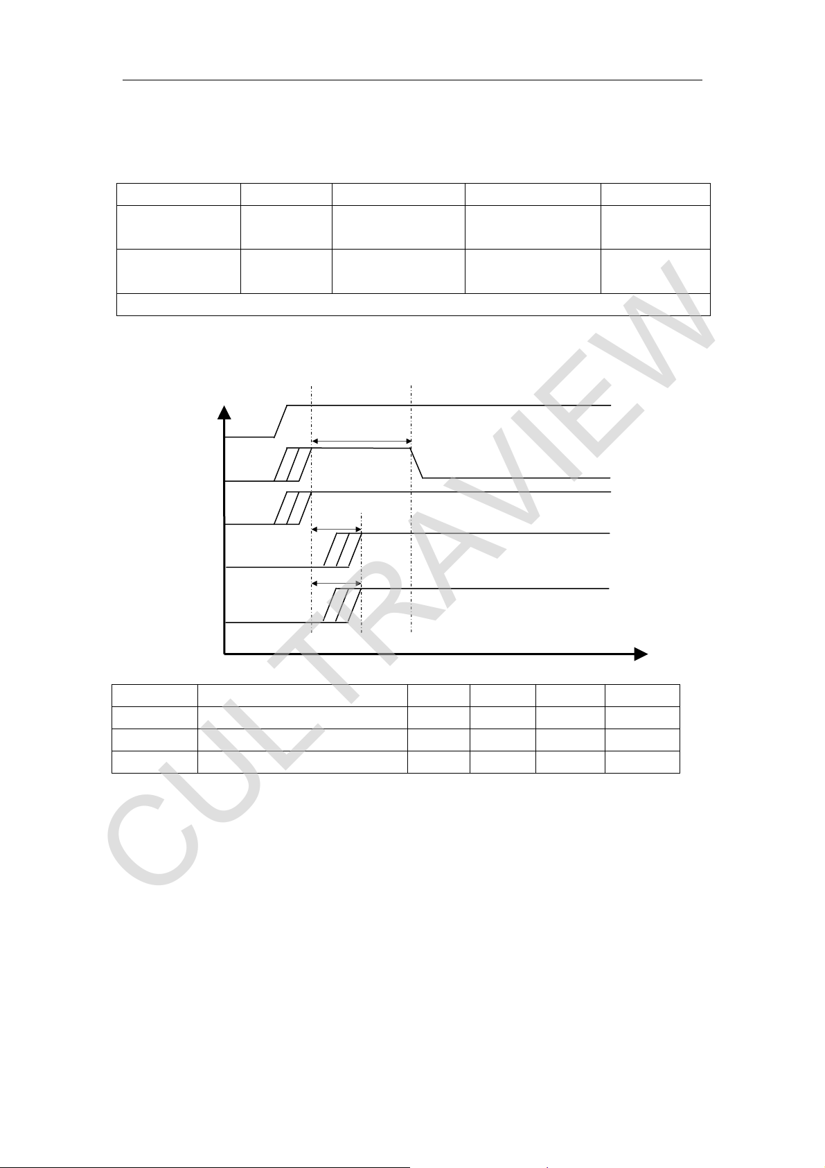
5. ELECTRICAL CHARACTERISTICS
Input Electrical Characteristics
Power Symbol Range Max Current Ripple
12V
(Ext .Adaptor)
12V
(Built in)
The current of panel, Inverter and extension modules are not included in max current.
Power Up Timing
POWER
HWRESET
PWR_ON/OFF
TIME
alternation DESCRIPTION Min Type Max Unit
+5Vstb
+5V
+12V
t1 Hardware Reste Width 10 200 / ms
t2 Pwr_on/off t
t3 Pwr_on/off t
+12V +12V--+12.5V 5A 100mV
+12V +12V--+12.5V 2A 100mV
t1
t2
t3
TO +5V t
setup
TO +12V t
setup
/ / 190 ms
setup
setup
/ / 190 ms
All rights reserve, if there is discrepancy,please refer to the actual product
7
Page 12
Shenzhen Cultraview Digital Technology CO., LTD
CULTRAVIEW
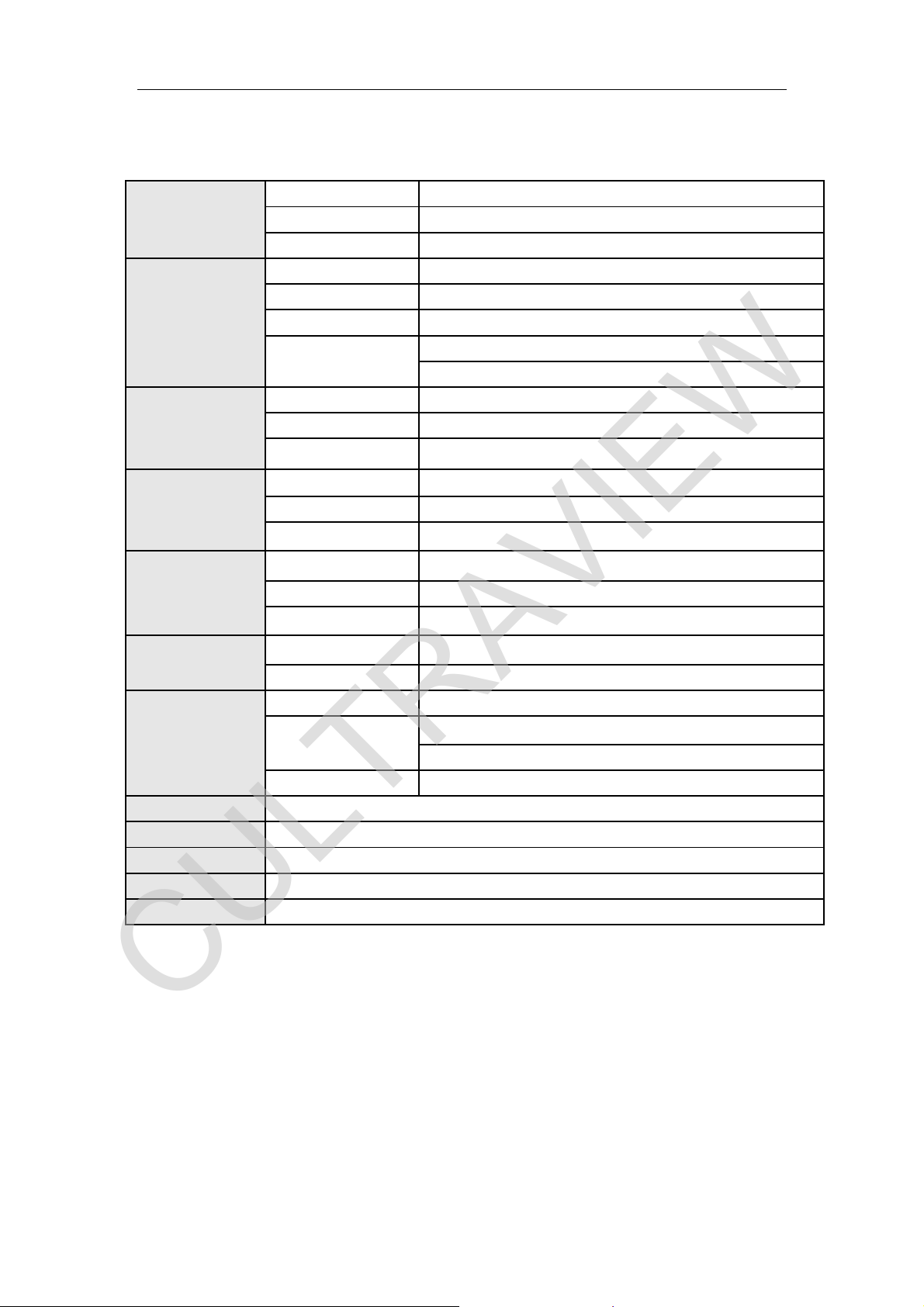
6. SUBSTITUTABLE PRIMARY MATERIALS
General materials
Including SMT capacitors, SMT resistors, diodes, transistors, MOSFET, connectors,
common inductance, electrolytic capacitor, PCB etc., and having no obvious
changes in appearance or color. Our company has two or three alternative suppliers
with these materials, maybe we will alternative use these materials for follow-up
mass production due to delivery time, stock or other reasons. We no longer notice
your company the alternative materials used. If necessary, you can apply for using
related materials (mention as above) in samples stage.
(Note: The alternative materials which have been accepted by our materials
confirmation department and PP will enter our system.)
Key materials
Including crystals, LDO, SAW Filter, DC-DC, Amplifier, Audio &Video switch, and
having obvious changes in appearance and color of general materials, Our company
has two or three alternative suppliers with these materials (See following table for
detail), maybe we will alternative use these materials for follow-up mass production
due to delivery time, stock or other reasons. We will notice your company the
alternative materials used in written form. If necessary, you can apply for using
related materials (mention as above) in samples stage.
Name Main Type Brand Backup Type Brand
LDO BL1117 BL
BM1117
BM
SY8120B Silergy BL8021 BL
DCDC
Audio
Amplifier
Crystal
Core materials
Including DDR, FLASH, TUNER, and the materials related to change software. Our
company has two or three alternative suppliers with these materials (See following
table for detail), maybe we will alternative use these materials for follow-up mass
production due to delivery time, stock or other reasons. We will notice your company
in written form and we must get your company confirm whether accept before using
the alternative materials.
MP1495 MPS -- --
NS4263 NSIWAY -- --
24MHz +-20PPM
20PF HC 49US
ZG
24MHz +-20PPM
20PF HC 49US
LS
TJ
All rights reserve, if there is discrepancy,please refer to the actual product
8
Page 13

Shenzhen Cultraview Digital Technology CO., LTD
CULTRAVIEW
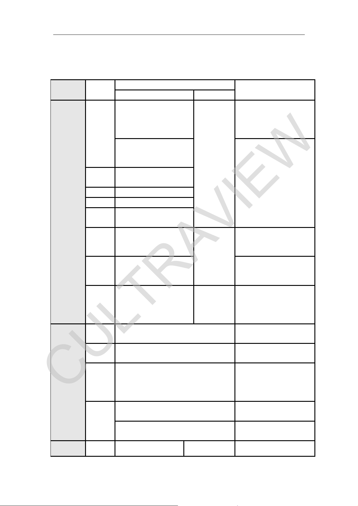
Name Main Type Brand BackupType Brand
Chipset TSUMV59/TSUMV29 MSTAR -- --
GD25Q32BSIG GD
W25Q32BVSSIG Winbond
W25Q32 WINBOND
FLASH
W25Q16CVSSIG Winbond
TUNER R620D Rafael
MX25L3206EM2I-12G MXIC
EN25Q32A EON
EN25Q32B EON
GD25Q16BSIG GD
EN25Q16 EON
-- --
-- --
All rights reserve, if there is discrepancy,please refer to the actual product
9
Page 14
Shenzhen Cultraview Digital Technology CO., LTD
CULTRAVIEW
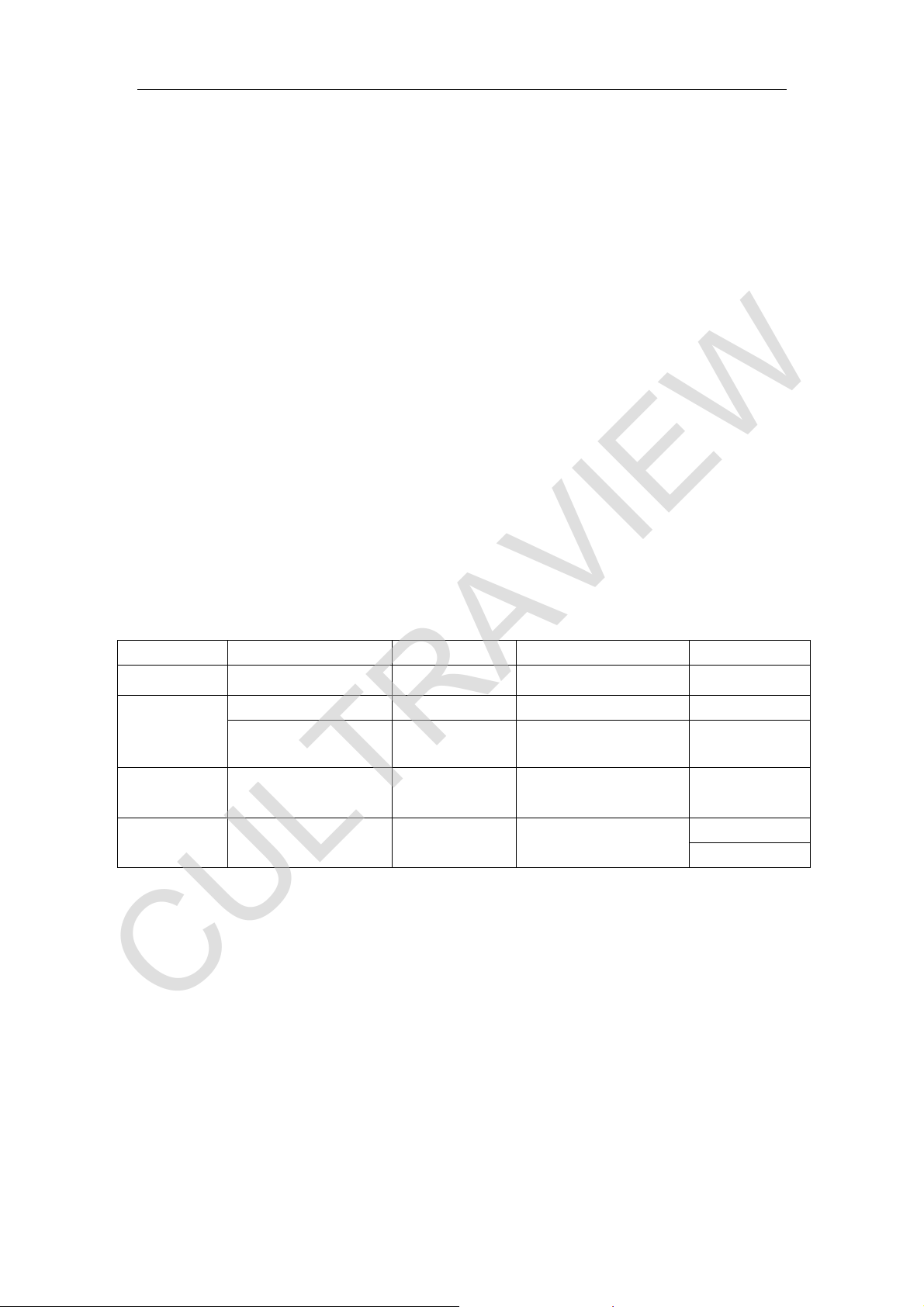
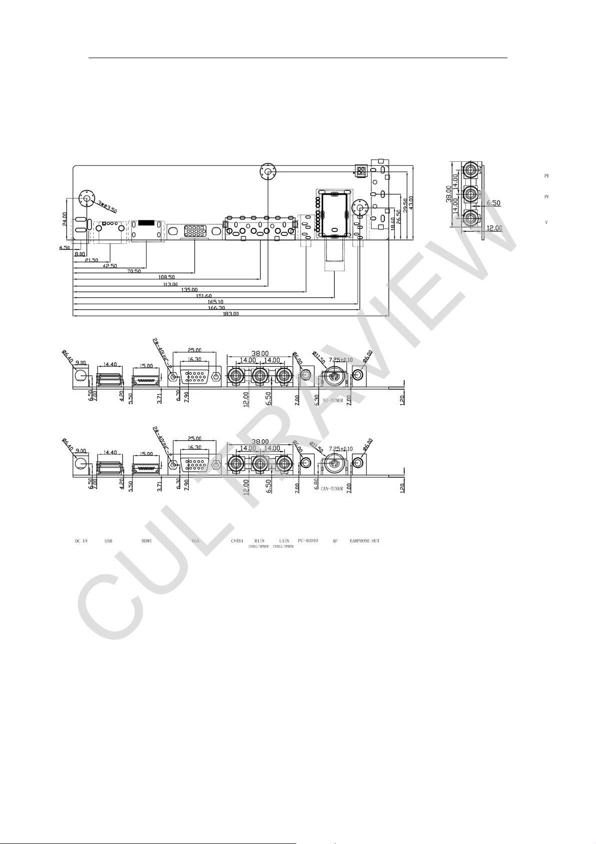
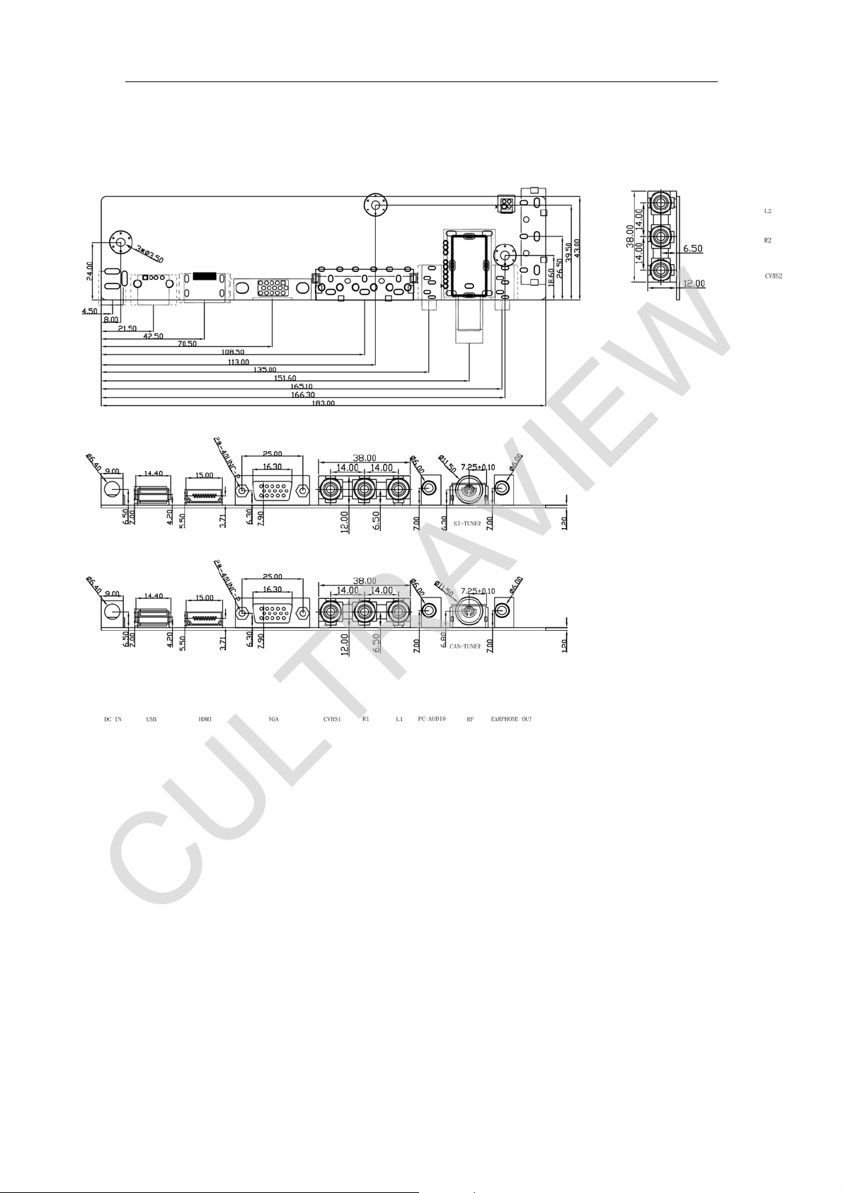
7. PICTURES
The picture is for a reference only,the actual item is the standard.
The optional connectors and terminals are marked with“*”.
Board Type 1:
TOP VIEW
*J8:
INVERTER
FRFRONT VIEW
DC-IN USB HDMI VGA
J1:
KEY&IR
*J2/J4:PANE
L POWER
J5:LVDS J6:SPEAKER
CVBS1 R1 L1
AV1 IN
PC
AUDIO
RF
IN
J9:
2
C INTERFACE
I
EARPHONE
SIDE VIEW
All rights reserve, if there is discrepancy,please refer to the actual product
Y Pb Pr
YPBPR
10
Page 15
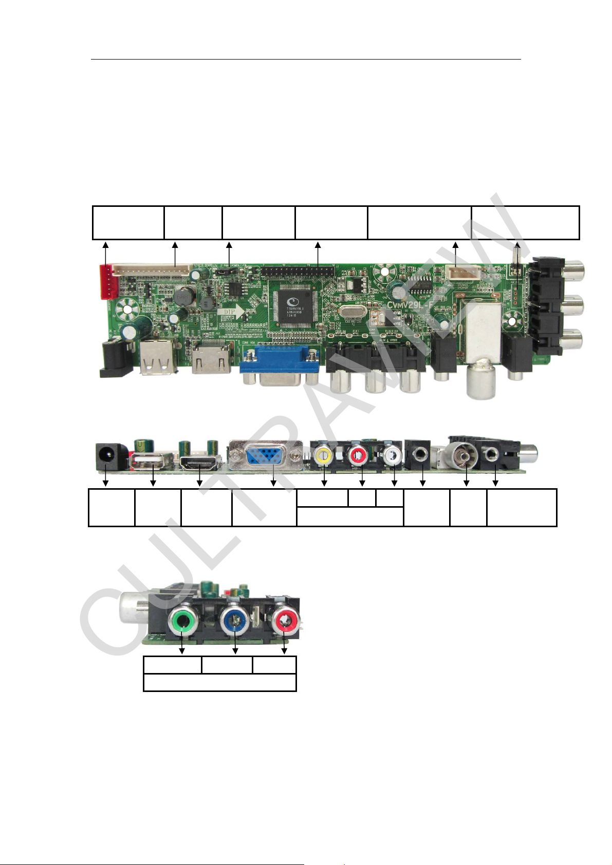
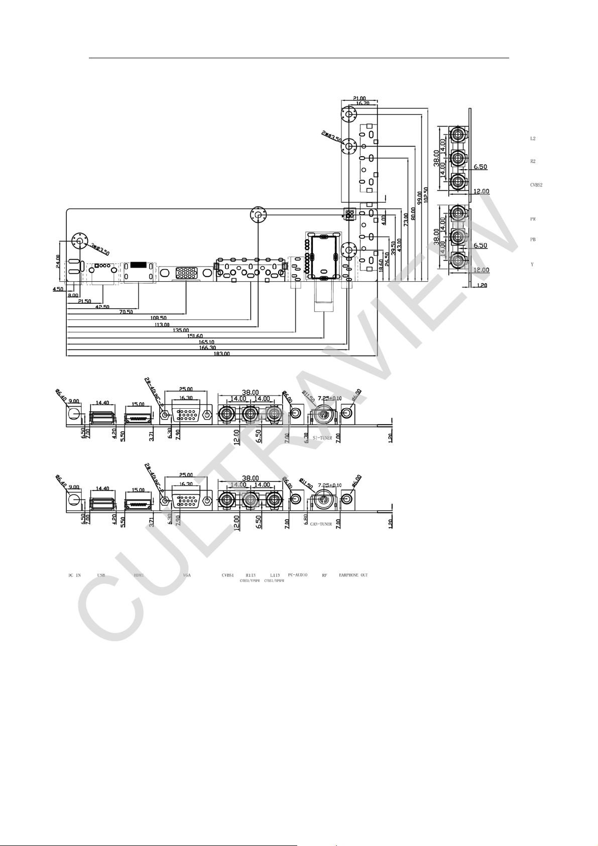
Board Type 2 :
CULTRAVIEW
TOP VIEW
FRONT VIEW
Shenzhen Cultraview Digital Technology CO., LTD
SIDE VIEW
CVBS2 R2 L2
AV2 IN
All rights reserve, if there is discrepancy,please refer to the actual product
11
Page 16
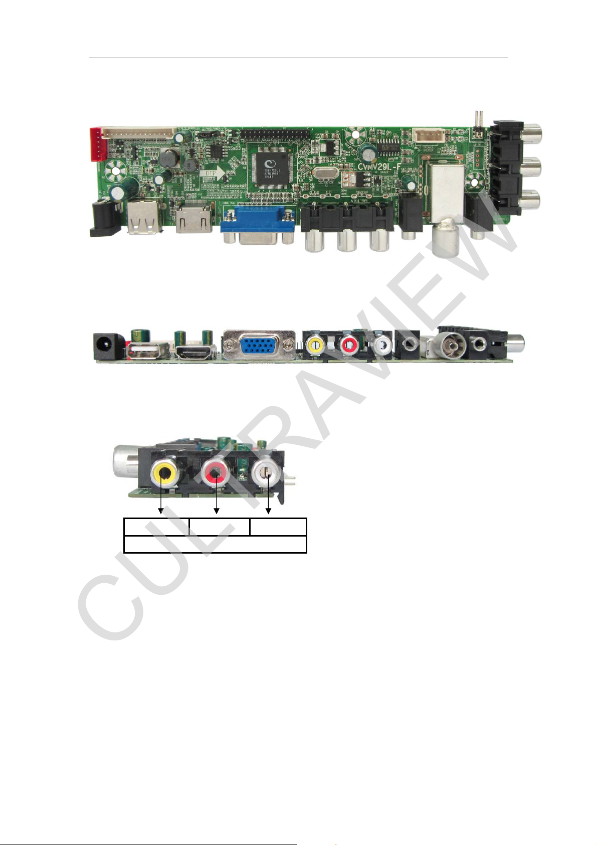
Board Type 3 :
CULTRAVIEW
TOP VIEW
FRONT VIEW
Shenzhen Cultraview Digital Technology CO., LTD
Expand Board Name :
CVAVIN -C-10-130323
Expand Port
AV
SIDE VIEW
Y PB PR CVBS2 R2 L2
YPBPR AV2 IN
All rights reserve, if there is discrepancy,please refer to the actual product
12
Page 17
Shenzhen Cultraview Digital Technology CO., LTD
CULTRAVIEW
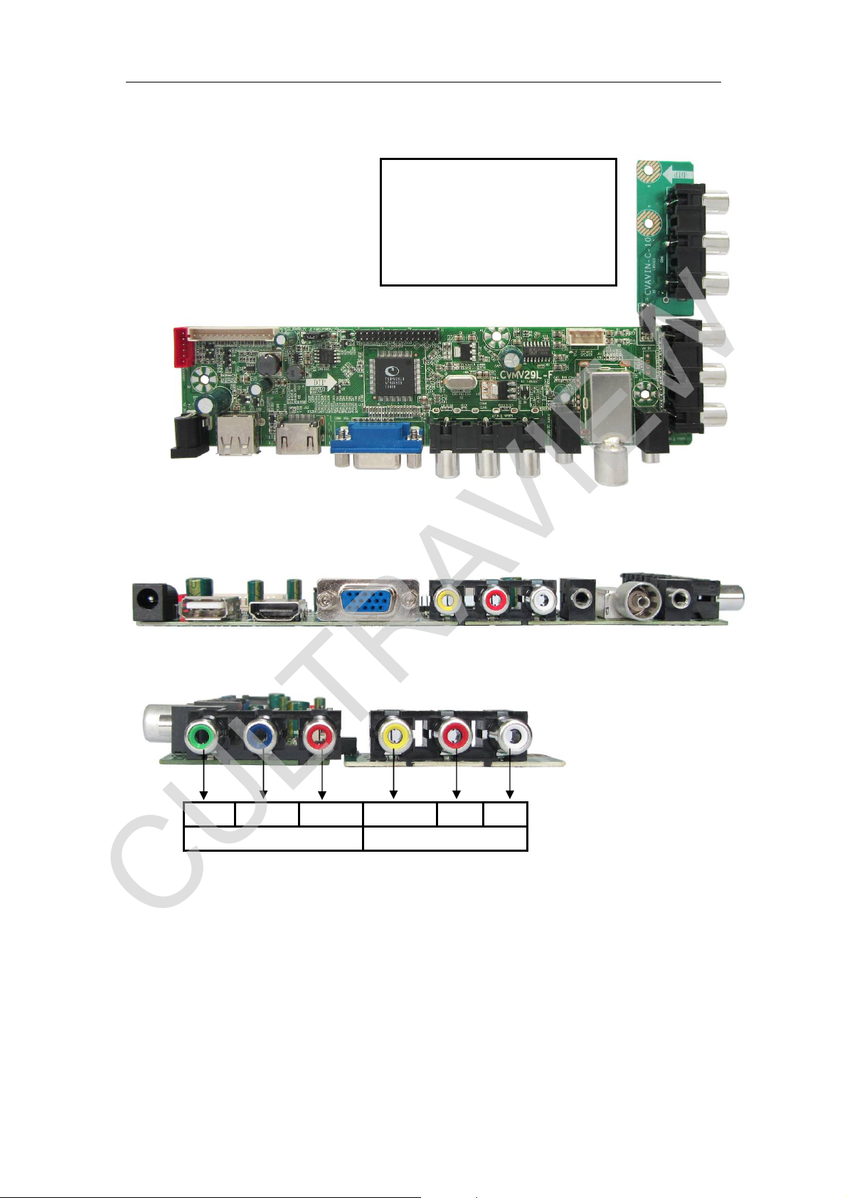
8. INTERFACE DEFINITION
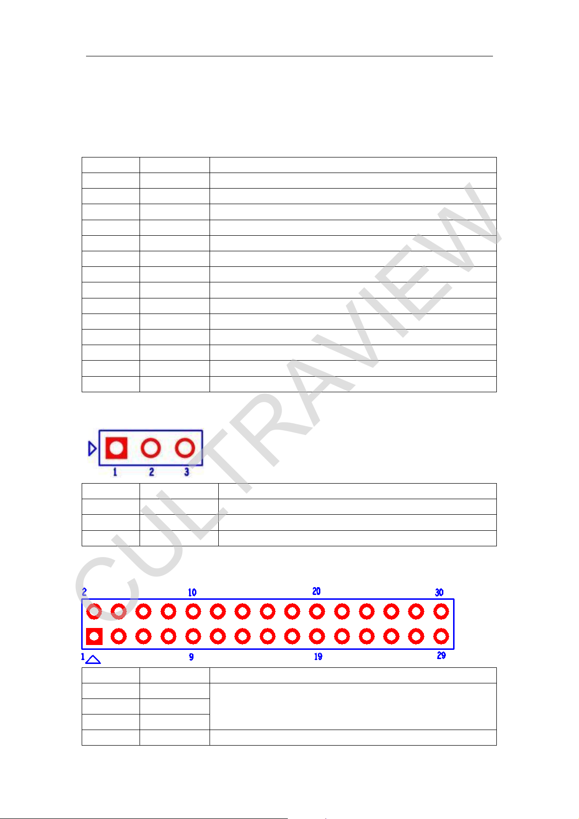
All jacks recognize the square pad as first pin.
J1: KEY&IR BOARD CONNECTOR(14PIN/2.0)
NO Definition Description
1 GND Ground
2 K7 (Reserved)
3 K6 POWER key
4 K5 RIGHT key
5 K4 LEFT key
6 K3 SOURCE key
7 K2 UP key
8 K1 DOWEN key
9 K0 MENU key
10 GND Ground
11 IR Remote receive
12 LED_G Green indicator
13 LED_R Red indicator
14 LED_5V +5V power
J2 : PANEL POWER SUPPLY(3PIN/2.54)
NO Definition Description
1 +3.3V +3.3V panel voltage
2 VCC_PANEL Panel Power In
3 +5V +5V panel voltage
J3: LVDS INTERFACE(2×15PIN/2.0)
NO. SYMBOL DESCRIPTION
1 VCC
2 VCC
3 VCC
4 GND Ground
Power Supply For Panel
All rights reserve, if there is discrepancy,please refer to the actual product
13
Page 18
Shenzhen Cultraview Digital Technology CO., LTD
CULTRAVIEW
5 GND Ground
6 GND Ground
7 RXO0- LVDS ODD 0- Signal
8 RXO0+ LVDS ODD 0+ Signal
9 RXO1- LVDS ODD 1- Signal
10 RXO1+ LVDS ODD 1+ Signal
11 RXO2- LVDS ODD 2- Signal
12 RXO2+ LVDS ODD 2+ Signal
13 GND Ground
14 GND Ground
15 RXOC- LVDS ODD Clock- Signal
16 RXOC+ LVDS ODD Clock + Signal
17 RXO3- LVDS ODD 3- Signal
18 RXO3+ LVDS ODD 3+ Signal
19 RXE0- LVDS EVEN 0- Signal
20 RXE0+ LVDS EVEN 0+ Signal
21 RXE1- LVDS EVEN 1- Signal
22 RXE1+ LVDS EVEN 1+ Signal
23 RXE2- LVDS EVEN 2- Signal
24 RXE2+ LVDS EVEN 2+ Signal
25 GND Ground
26 GND Ground
27 RXEC- LVDS EVEN Clock- Signal
28 RXEC+ LVDS EVEN Clock + Signal
29 RXE3- LVDS EVEN 3- Signal
30 RXE3+ LVDS EVEN 3+ Signal
J5 : SPEAKER CONNECTOR(4PIN/2.54)
NO. SYMBOL DESCRIPTION
1 ROUT+ Audio Right channel Output+
2 ROUT- Audio Right channel Output-
3 LOUT- Audio Left channel Output-
4 LOUT+ Audio Left channel Output+
J7: SPEAKER CONNECTOR(4PIN/2.0)
NO. SYMBOL DESCRIPTION
1 ROUT+ Audio Right channel Output+
2 ROUT- Audio Right channel Output-
3 LOUT- Audio Left channel Output-
4 LOUT+ Audio Left channel Output+
J8: INVERTER interfaces(6PIN/2.0)
NO Definition Description
All rights reserve, if there is discrepancy,please refer to the actual product
14
Page 19
Shenzhen Cultraview Digital Technology CO., LTD
CULTRAVIEW
1 GND Ground
2 GND Ground
3 ADJ Brightness Adjustment for Panel(Volts DC Output)
4 BL_ON Back-Light ON/OFF Control for Panel
5 +12V INVERTER +12V DC Power Supply
6 +12V INVERTER +12V DC Power Supply
2
J9:EXTERNAL I
NO. SYMBOL DESCRIPTION
1 +5V +5V DC Power Supply
2 SCL External I2C SCL
3 SDA External I2C SDA
4 GND Ground
J10: EXTERNAL USB CONNECTOR(4PIN/2.0)
NO. SYMBOL DESCRIPTION
1 GND Ground
2 DP USB Data+
3 DM USB Data-
4 +5V +5V Power Supply for USB
C CONNECYOR
All rights reserve, if there is discrepancy,please refer to the actual product
15
Page 20
Shenzhen Cultraview Digital Technology CO., LTD
CULTRAVIEW
9. CONFIGURATION
Board Type 1:
NTSC RF Connect is φ 9.5mm
The thickness of PCB board: 1.2 mm
Component the tallest altitude: 12.5 mm
Install diameter inside the bore 3.5 mm
All rights reserve, if there is discrepancy,please refer to the actual product
16
Page 21
Board Type 2 :
CULTRAVIEW
Shenzhen Cultraview Digital Technology CO., LTD
NTSC RF Connect is φ 9.5mm
The thickness of PCB board: 1.2 mm
Component the tallest altitude: 12.5 mm
Install diameter inside the bore 3.5 mm
All rights reserve, if there is discrepancy,please refer to the actual product
17
Page 22
Board Type 3:
CULTRAVIEW
Shenzhen Cultraview Digital Technology CO., LTD
NTSC RF Connect is φ 9.5mm
The thickness of PCB board: 1.2 mm
Component the tallest altitude: 12.5 mm
Install diameter inside the bore 3.5 mm
All rights reserve, if there is discrepancy,please refer to the actual product
18
Page 23

ShenZhen Cultraview Digital Technology CO.,LTD
CULTRAVIEW
10. APPLICATION REQUIREMENT
¾ Relative humidity ≤80%
¾ Store temperature -10~+60 ℃
¾ Use temperature 0~+40 ℃
¾ The procedure of the whole machine assembles and transports need to
attend ESD transaction.
¾ When the whole set assemble, it can down pack or side pack, but don't
make the board transform or distort, don't be subjected to heavy pressure.
¾ The hole of each port does not be opened too small, especially the HDMI
port hole, avoid the whole set morphing to cause the extrusion of port when
installing.
¾ The hole of RGB socket is recommended the situation of not using the
screw stationary on the RGB socket to fix on the structure board.
¾ The connected wire which between the other boards and this board can't be
leaded too long, or affect performance and image quality.
¾ The whole set inner wires matching reasonable, each connected wire try to
not directly cross the PCB board, especially cross over from the main IC,
avoid affect the whole set EMC performance.
¾ n order to obtain better EMC effect of the whole set, we suggest the LVDS
twisted pair wire between the main board and panel must be tied up well
and try to use shielding wire. If it’s possible, try to put on the magnetic belt
ring on the wire which near the board terminal.
¾ The HDMI and HDCP on the main board are all passed the related
certifications, but we just provide testing certification of the inner usage
standard. If you need to use legal HDMI and HDCP, please apply related
association as formal member by yourself.
¾ There is ROHS identification on the board and package, the board match
ROHS standard.
All rights reserve, if the specification has fluctuation and take real object as quasi
19
Page 24

ShenZhen Cultraview Digital Technology CO.,LTD
CULTRAVIEW
11. EXCURSUS
Keyboard and remote definition
All rights reserve, if the specification has fluctuation and take real object as quasi
20
Page 25

5
4
3
2
1
POWER
IN
J14
J14
DC3AIN
DC3AIN
GND
POWER
GND
POWER
123
GND
D D
C C
B B
GND
3.3VU 1.2VU
U7 BL1117-ADJU7 BL1117-ADJ
3
VIN
1
U2 BL1117-ADJU2 BL1117-ADJ
3
VIN
C43
C43
100nF
100nF
12VU3.3VU
PWR-ON/OFF
L:ON
H:OFF
GND
3
1
C29
C29
100nF
100nF
5VA 2.5VA
C90
C90
10uF
10uF
5VU
Inverter Interface
(预留)防止上电闪白屏
VBL_CTRL
VBL_CTRL3
A A
BRI_ADJ-PWM03
BRI_ADJ-PWM0
TP5
TP5
12VU
12VU
12VU12VIN
1
12
CA5
CA5
C89
C89
470uF
470uF
100nF
100nF
TP4
TP4
1.32VU
1.32VU
C65
C65
10uF
10uF
C32
C32
100nF
100nF
C75
C75
10uF
10uF
TP1
TP1
2.5VA
2.5VA
1
C8
10uFC810uF
1
C68
C68
100nF
100nF
2
VOUT
4
TAB
R87NCR87
NC
R91 0RR91 0R
1.8VA
2
VOUT
4
Vout1
ADJ
R64
R64
200R_1%
1
200R_1%
R1
R63
R63
R2 Vo=1.25*(1+R2/R1)
200R_1%
200R_1%
TSUMV29,39LU,R1=R2=200R,for
DDR1供电
V59,R1=200R;R2=100R,for DDR2供电
J6J6
+12V1VCC-Panel
+5V
+12V
J2J2
5
VCC-Panel
R30 4.7KR30 4.7K
1.5K 改为2.2K
5VU
R58
R58
4.7K
4.7K
R59 4.7KR59 4.7K
R39 4.7KR39 4.7K
2
2
5VA
R47 4.7KR47 4.7K
R25
R25
47K
47K
R24 200KR24 200K
Q2
MMBT3904Q2MMBT3904
1
2 3
R29
R29
2.2k
2.2k
5VA
R48
R48
R491KR49
47K/NC
47K/NC
1K
1
2 3
Q3
1
MMBT3904Q3MMBT3904
2 3
5VU 5VA
Q9 3407Q9 3407
3
R89
R89
47K
47K
3.3VU
R33
R33
10K
10K
PWR-ON/OFF
PWR-ON/OFF3
R96 4.7KR96 4.7K
H:ON
L:Standby
1
R90 100KR90 100K
R93
R93
4.7K
4.7K
Q10
Q10
MMBT3904
MMBT3904
2 3
C72
C72
100nF
100nF
2
1
TP6
TP6
1
5VA
5VA
3.3VU 3.3VA
Q8 3407Q8 3407
3
2
1
1、针对单12V输入的电源,L27 ,L29 NC,L28装0R
2、针对单12V和5V同时长供的电源,L27,L29 NC,L28装0R
3、针对12V和5V可控的内置电源,L27,L29 装0R,L28 NC, 注意5V转换电路和系统5V开关电路需要NC
SY8113改用MP1495
12VU
R38 75RR38 75R
Q5
MMBT3904Q5MMBT3904
R26 4.7KR26 4.7K
C7
10uFC710uF
Q1 3407Q1 3407
2
C4
100nFC4100nF
C31
C31
100nF/NC
100nF/NC
C22
C22
100nF
100nF
4
PB-ON/OFF
PB-ADJUST
VCC-Panel
1
12VIN
PB-ADJUST
3
PB-ON/OFF
6
5
4
3
2
1
PH-6AJ8PH-6A
+12V1
+12V
ON/OFF
ADJ
GND1
GND
J8
+5V_SB
C61
C61
C57
C57
R52
R52
100K
100K
3
100nF
100nF
C40
C40
100nF
100nF
10UF
10UF
R55
R55
100K
100K
R75
R75
11K
11K
A1
AHOLE138A1AHOLE138
1
orientpadM4orientpad
100uF/16V
100uF/16V
1
M4
12VU
CA1
CA1
12
A2
AHOLE138A2AHOLE138
1
U5
2
IN
6
EN
7
VCC
1
AAM
MP1495DJU5MP1495DJ
R31 100KR31 100K
C35
C35
100nF
100nF
A3
AHOLE138A3AHOLE138
1
M3
1
orientpadM3orientpad
GND
4
C30
C30
100nF/NC
100nF/NC
1
orientpadM2orientpad
2
5
BST
R53 10RR53 10R
3
SW
8
FB
C46 100nFC46 100nF
U4
U4
1
BS
LX
SY8120B--2A
SY8120B--2A
5
IN
SY8113----3A
SY8113----3A
4
FB
EN
GND
2
Size Document Number Rev
Size Document Number Rev
Size Document Number Rev
M2
Date: Sheet
Date: Sheet
Date: Sheet
C33
C33
100nF
100nF
L8 6.8uH/3.1AL8 6.8uH/3.1A
R51 33K/1%R51 33K/1%
L12 6.8uH/2AL12 6.8uH/2A
6
3
Custom
Custom
Custom
02.Power
02.Power
02.Power
Vout=0.8(1+R1/R2)
R44
R44
62K_1%
62K_1%
R43
R43
11.5K_1%
11.5K_1%
Vout= 0.6*(1+R65/R66)
12
R1
CA3
CA3
100uF/16V
100uF/16V
R2
Vout= 0.8*(1+R1/R2)
TP2
TP2
3.3VU
3.3VU
3.3VU
1
R32
R32
47K_1%
47K_1%
C20
C20
C44
C44
R35
R35
100nF
100nF
10uF-X5R
10uF-X5R
10.2K_1%
10.2K_1%
Title
Title
Title
CVMV29L-F-10
CVMV29L-F-10
CVMV29L-F-10
1
TP3
TP3
5VU
5VU
1
10uF-X5R
10uF-X5R
27Monday, March 25, 2013
27Monday, March 25, 2013
27Monday, March 25, 2013
C64
C64
5VU
C63
C63
10uF-X5R
10uF-X5R
C39
C39
10uF-X5R
10uF-X5R
of
of
of
C62
C62
100nF
100nF
1.0
1.0
1.0
Page 26

5
4
3
2
1
4
4
4
4
4
4
4
4
4
MAIN IC Chip
RESET
3.3VU
Q7
SGM810Q7SGM810
1
C34
C34
100nF
D D
C C
B B
100nF
晶振负载电容确定
XTALI
XTALO
3.3VU
U3 GD25Q16BU3 GD25Q16B
8
VDD
7
HOLD#
SPI_Flash-SCK
6
CLK
SPI_Flash-SDI
5
DI
主IC选用TSUMV39LU时,具有MM功能,默认使
1MByte的Flash,如果有需要,可以使用2MByte;
如果不使用MM功能,则Flash默认为512K。
主IC选用TSUMV29LU时,不具有MM功能,默认
使用512KByte。
DEBUG PORT
5VU
R81
R81
4.7K/NC
4.7K/NC
23
R821MR82
WP#
VSS
R78
R78
4.7K/NC
4.7K/NC
1M
CE#
SO
UART-RX
UART-TX
R84
R84
100K
100K
1
2
3
4
R85 1KR85 1K
C60 33pFC60 33pF
12
Y2
3
24MHZY224MHZ
C59 33pFC59 33pF
SPI_CS0N
SPI_Flash-SDO
FLASH_WP0N
UART-RX 5
UART-TX 5
R28
R28
4.7K
4.7K
3.3VU
C48
C48
100nF
100nF
R651KR65
1K
System-RST
FLASH
VGA_HS5
RGB0_Pb+5
RGB0_Y-SOG5
RGB0_Y+5
RGB0_Pr+5
VGA_VS5
ADC2P5
RGB2-HDTV_BIN5
RGB2-HDTV_SOGIN5
RGB2-HDTV_GIN5
RGB2-HDTV_RIN5
AV2-CVBS2P5
AV1-CVBS1P5
SC-AULin05
SC-AURin05
VDD33
VDDC
VGA_HS
RGB0_Pb+
RGB0_Y-SOG
RGB0_Y+
R121 68RR121 68R
RGB0_Pr+
VGA_VS
RGB2-HDTV_BIN
RGB2-HDTV_SOGIN
RGB2-HDTV_GIN
R123 68RR123 68R
RGB2-HDTV_RIN
AVDD33_OR_HSYNC1
AV2-CVBS2P
AV1-CVBS1P
R124 68RR124 68R
AU33
SC-AULin0
Close to IC
with width trace
C102 47nFC102 47nF
C103 1nFC103 1nF
C104 47nFC104 47nF
C105 47nFC105 47nF
C106 47nFC106 47nF
C113 47nFC113 47nF
C92 1nFC92 1nF
C93 47nFC93 47nF
C94 47nFC94 47nF
C95 47nFC95 47nF
C96 47nFC96 47nF
C97 47nFC97 47nF
C98 47nFC98 47nF
C110 1uC110 1u
C91 1uC91 1u
C78
C78
100nF
100nF
L16
L16
120R/FB
120R/FB
U6
U6
110
111
1
2
BIN0
SOGIN0
GIN0P
GIN0M
RIN0
BIN2
SOGIN2
GIN2P
GIN2M
RIN2
CVBS1
CVBS0
VCOM0
AUVAG
C80
C80
10uF
10uF
3
4
5
6
7
8
9
10
11
12
13
14
15
16
17
18
19
20
21
22
AUL0
23
AUR0SC-AURin0
24
25
HDMI1-RX2P
HDMI1-RX2N
HDMI1-RX2P
100
101
102
103
104
105
99
NC0
RX2P
NC1
E-Pad1
E-Pad2
E-Pad3
E-Pad4
E-Pad5
AVDD_330
VDDC
HSYNC0
BIN0P
SOGIN0
GIN0P
GIN0M
RIN0P
VSYNC0
AVDD_25
BIN1P
SOGIN1
GIN1P
GIN1M
RIN1P
MST6M182XX/TSUMV39LU
AVDD_331
CVBS2
CVBS1
CVBS0
VCOM
CVBSOUT
AVDD_AU33
AUL0
AUR0
AUVAG
AUL426AUR427AUL528AUR5
TSUMV39LU
TSUMV39LU
AUL4
AUR4VGA-AURin2
C811u C811u
C831u C831u
VGA-AULin2
VGA-AULin2
4
HDMI1-RX0P
HDMI1-RX1P
HDMI1-RX2N
HDMI1-RX0N4HDMI1-CLKP
HDMI1-RX1N
HDMI1-SCL
HDMI1-SCL
HDMI1-SDA
HDMI1-RX1N
HDMI1-RX1P
97
98
96
RX1P
RX1N
RX2N
DDCD_CK
TSUMV39LU
TSUMV39LU
HDMI-CEC
HDMI1-CLKN
HDMI_HP1
HDMI1-SDA
HDMI1-CLKP
HDMI1-RX0N
HDMI1-RX0P
94
92
95
93
RX0P
RX0N
DDCD_DA
HDMI1-CLKN
91
RXCKP
HDMI_HP1
90
RXCKN
GND-EFUSE
89
HOTPLUGD
System-RST
88
GND_EFUSE
HDMI-CEC
87
HWRESET
AVDD_DDR_2.5V/1.8V
UART-TX
IRIN
KEY0-SAR0
UART-TX
85
84
86
83
IRIN
CEC
SAR1
SAR0
DDCA_DA82DDCA_CK
AVDD_DDR
TSUMV29LU
TSUMV29LE
VDDIO_CMD
XTALO
5
AMP_RIN
VIFM39RFAGC
AVDD_REF37VIFP38GPIO5643GPIO5744AVDD_PLL45VDD0
41
40
36
VIFP
VIFM
XTALI
AGC
5
5
5
7
7
VIFP
VIFM
AVDD_DMPLL
AVDD25_DEMOD
AVDD_DDR_2.5V/1.8V
GPIO55
42
TUNER_SCL
TUNER_SDA
LED
AUL5
C761u C761u
AV1-AULin5
VGA-AURin2
AUOUTL030AUOUTR031AUOUTL132AUOUTR133XOUT34XIN35AVDD_DMPLL
29
C731u C731u
AV1-AURin5 AUR5
AMP_LIN
AV1-AULin5
AV1-AURin5
AMP_RIN
AMP_LIN
UART-RX
UART-RX
R7768R R7768R
81
KEYBOARDLED IR
PH-14AJ1PH-14A
5V_LED
A A
LED_R
LED_G
POWER
Reserved
J1
REMOTE
+5V
IR
GND1
MENU
CH-
CH+
INPUT
VOL-
VOL+
GND
R40 33RR40 33R
5V_LED
14
13
12
11
10
9
8
7
6
5
4
3
2
1
C451uC45
1u
LED_R
LED_G
REMOTE
MENU K0
DOWN/CH- K1
UP/CH+ K2
INPUT K3
RIGHT/V+ K5
5VU
C17
C17
100nF
100nF
5
R15 68RR15 68R
K4LEFT/VK6POWER
K7EXIT
C19
C19
33pF
33pF
IRIN
5VU
R12 10KR12 10K
REMOTE
R14 510RR14 510R
2.51V
0.417V
0.873V
1.286V
1.65V
2.1V
0.007V
0.007V
K0
R16 20KR16 20K
K1
R17 820RR17 820R
K2
R18 1.5KR18 1.5K
K3
R19 3KR19 3K
K4
R20 4.7KR20 4.7K
K5
R21 8.2KR21 8.2K
K6
R22 33RR22 33R
K7
R23 33RR23 33R
39K 2.95V
LED_GLED
R11 4.7KR11 4.7K
R133KR13
3K
3.3VU
R80
R80
4.7K
4.7K
KEY0-SAR0
C18
C18
100nF
100nF
5VU
R41
R41
1.5K
1.5K
LED_R
Q4
1
MMBT3904Q4MMBT3904
2 3
4
Tuner Connector
+3V3_TUNER
R34
R34
10K
10K
TAGC
C47
C47
22nF
22nF
R36 10KR36 10K
3
TAGC6
2
4
5
5
USB1_D-
MUTE_AMP
BRI_ADJ-PWM0
USB1_D+
USB1_DM
USB1_DP
MUTE_AMP
BRI_ADJ-PWM0
R7368R R7368R
106
107
108
79
78
76
77
E-Pad6
E-Pad7
TESTPIN
USB0_DP
USB0_DM
PWM1/GPIO2580PWM0/GPIO26
INT/GPIO65
AVDD_MOD1
LVBCKM
LVBCKP
AVDD_MOD0
LVACKP
LVA3P47LVA3M48LVACKM
49
50
46
LVRXO0- RXO0LVRXO0+ RXO0+
LVRXO1- RXO1LVRXO1+ RXO1+
LVRXO2- RXO2LVRXO2+ RXO2+
LVRXO3- RXO3LVRXO3+ RXO3+
LVRXE0- RXE0LVRXE0+ RXE0+
LVRXEC-
LVRXE3+
LVRXEC+
LVRXE3-
LVRXE1- RXE1LVRXE1+ RXE1+
6
6
LVRXE2- RXE2LVRXE2+ RXE2+
VDDC
AVDD_PLL
LVRXE3- RXE3LVRXE3+ RXE3+
AGC
7
4
4
TSUMV29LU没有USB。
109
E-Pad8
E-Pad9
75
SCZ
74
SDO
73
SDI
72
SCK
71
GPIO0
70
69
VDD1
68
LVBOM
67
LVB0P
66
LVB1M
65
LVB1P
64
63
LVB2M
62
LVB2P
61
60
59
LVB3M
58
LVB3P
57
LVA0M
56
LVA0P
55
LVA1M
54
LVA1P
53
LVA2M
52
LVA2P
51
去掉排阻
SPI-CS0N SPI_CS0N
SPI-SDO SPI_Flash-SDO
SPI-SDI SPI_Flash-SDI
SPI-SCK SPI_Flash-SCK
VBL_CTRL
PWR-ON/OFF
LVRXO0LVRXO0+
LVRXO1LVRXO1+
LVRXO2LVRXO2+
LVRXOCLVRXOC+
LVRXO3LVRXO3+
LVRXE0LVRXE0+
LVRXE1LVRXE1+
LVRXE2LVRXE2+
RXOC-LVRXOCRXOC+LVRXOC+
RXEC-LVRXECRXEC+LVRXEC+
TUNER_SCL
TUNER_SDA
VBL_CTRL 2
PWR-ON/OFF 2
VDDC
AVDD_MOD
AVDD_MOD
TUNER_SCL 6
TUNER_SDA 6
IC Power
Close to IC
2.5VA
1.8VA
3.3VU
2.5VA
L106
L4 120R/FBL4 120R/FB
L5 120R/FB/NCL5 120R/FB/NC
L107
V29,V39 L106=FB,L107=NC;
V59 L106=NC,L107=FB
3.3VU
1.2VU
Normal Power 3.3V
VDD33
Normal Power 1.2V
VDDC
C671uC67
1u
L101
R50 0R/NCR50 0R/NC
ADC2P5
C101
C101
100nF
100nF
C107
C107
100nF
100nF
C66
C66
C16
C16
100nF
100nF
100nF
100nF
AVDD_DDR_2.5V/1.8V
C53
C53
C36
C36
C104 C105
C25
C25
100nF
100nF
C108
C108
100nF
100nF
100nF/NC
100nF/NC
AVDD_PLL
C56
C56
100nF
100nF
VDD33
1u/NC
1u/NC
3.3VU
V29L101,C104和C105建议NC
掉
2.5VA
L3 120R/FBL3 120R/FB
L6 120R/FB/NCL6 120R/FB/NC
AVDD_MOD
C26
C26
100nF
100nF
L19 120R/FBL19 120R/FB
CHIP_CONFIG
{IPAD_PWM1, PAD_PWM0}
2
B51_NO_EJ
MUTE_AMP BRI_ADJ-PWM0
R62 4.7KR62 4.7K
4'h00
R67 4.7KR67 4.7K
RXE3+
RXEC+
C28 4.7pFC28 4.7pF
RXE2+
RXE1+
RXO3+
RXOC+ RXOC-
C23 4.7pFC23 4.7pF
RXO2+
RXO1+
30
28
26
24
22
20
18
16
14
12
10
8
6
4
2
HEAD 2x15_LVDS
HEAD 2x15_LVDS
RXE3+
RXEC+
GND6
RXE2+
RXE1+
RXE0+
RXO3+
RXOC+
GND4
RXO2+
RXO1+
RXO0+
GND2
GND
VCC1
J3
J3
Size Document Number Rev
Size Document Number Rev
Size Document Number Rev
Date: Sheet
Date: Sheet
Date: Sheet
,V39,V59
要上件
AVDD25_DEMOD
L103
L105
C55
C55
V29,V39L103=FB,L105=NC,
100nF
100nF
V59,L103=NC,L105=FB,
C42
C42
100nF
100nF
3.3VU
3.3VU
L102
AVDD33_OR_HSYNC1
C109
C109
100nF
100nF
TSUMV29,39LU L102=FB,MST6M182XX
L102=NC,主要是做SCART 信号的FS输入
RXE3-
29
Custom
Custom
Custom
RXE3RXEC-
GND5
RXE2RXE1RXE0RXO3RXOC-
GND3
RXO2RXO1RXO0-
GND1
VCC2
VCC
27
25
23
21
19
17
15
13
11
9
7
5
3
1
03.TSUMV39LU
03.TSUMV39LU
03.TSUMV39LU
RXECRXE2-
RXE1RXE0-RXE0+
RXO3-
RXO2RXO1RXO0-RXO0+
1
C15
C15
100nF
100nF
Title
Title
Title
AVDD_DMPLL
L13 120R/FBL13 120R/FB
C58
C58
100nF
100nF
AU33
C99
C99
100nF
100nF
C21 4.7pFC21 4.7pF
C24 4.7pFC24 4.7pF
VCC-Panel
CVMV29L-F-10
CVMV29L-F-10
CVMV29L-F-10
37Monday, March 25, 2013
37Monday, March 25, 2013
37Monday, March 25, 2013
of
of
of
1.0
1.0
1.0
Page 27

5
J12
J12
21
D D
22
23
20
C C
DATA2+
21
DATA2_SHIELD
DATA2-
DATA1+
DATA1_SHIELD
DAT1A-
DATA0+
22
DATA0_SHIELD
DATA0-
CLK_SHIELD
23
CEC_GND
+5V POWER
HOT PLUG
20
HDMI
HDMI
CLK+
CLK-
CEC
NC
SCL
SDA
1
2
3
4
5
6
7
8
9
10
11
12
13
14
15
16
17
18
19
MMBT3904
MMBT3904
HDMI1-RX2+ HDMI1-RX2P
HDMI1-RX2- HDMI1-RX2N
HDMI1-RX1+ HDMI1-RX1P
HDMI1-RX1- HDMI1-RX1N
HDMI1-RX0+ HDMI1-RX0P
HDMI1-RX0- HDMI1-RX0N
HDMI1-RXC+ HDMI1-CLKP
HDMI1-RXC- HDMI1-CLKN
CEC
HDMI1/5V
R1111KR111
1K
HDMI1-HPD
HDMI1-DDC-SCL
Q11
Q11
2 3
R107 4.7KR107 4.7K
1
4
R106 220R/NCR106 220R/NC
R108
R108
R135
R135
10K
10K
10K
10K
HDMI-CEC
R127
R127
10K
10K
R109 33RR109 33R
R110 33RR110 33R
HDMI1-RX2P 3
HDMI1-RX2N 3
HDMI1-RX1P 3
HDMI1-RX1N 3
HDMI1-RX0P 3
HDMI1-RX0N 3
HDMI1-CLKP 3
HDMI1-CLKN 3
HDMI-CEC 3
HDMI1-SCL
HDMI1-SDAHDMI1-DDC-SDA
HDMI_HP1
3
HDMI1-SCL 3
HDMI1-SDA 3
HDMI_HP1 3
2
USB_5V
USB1_D-3
USB1_D+3
USB1_DUSB1_D+
5VA USB_5V
PH-4A_USB/NC
PH-4A_USB/NC
4
+5V
3
DM
2
DP
1
GND
J10
J10
+5V
+5V
DM
DM
DP
DP
GND
GND
1
2
3
1
J13
J13
1
2
3
447
USB-H
USB-H
GND
GND
6
6
GND
GND
5
C79
C79
C9
100nF
100nF
B B
A A
Size Document Number Rev
Size Document Number Rev
Size Document Number Rev
Custom
Custom
Custom
Date: Sheet
Date: Sheet
5
4
3
Date: Sheet
2
10uFC910uF
Title
Title
Title
04.HDMI&USB
04.HDMI&USB
04.HDMI&USB
CVMV29L-F-10
CVMV29L-F-10
CVMV29L-F-10
of
of
of
47Monday, March 25, 2013
47Monday, March 25, 2013
47Monday, March 25, 2013
1
1.0
1.0
1.0
Page 28

5
CON6
CON6
GND
GND
VGA
VGA
10
GND
GND
5
15
SCL
SCL
V
V
H
H
SDA
SDA
NC
NC
D D
GND
GND
9
NC
NC
4
14
NC
NC
8
GND
GND
3
13
B
B
7
GND
GND
2
12
G
G
6
GND
GND
1
11
R
R
GND
GND
16 17
4
B
G
R
3
VGA-B
VGA-G
VGA-R
R128
R128
R132
R132
R131
R131
75R
75R
75R
75R
75R
75R
2
VGA-B
R112 33RR112 33R
VGA-G
R114 33RR114 33R
R113 33RR113 33R
VGA-R
R115 33RR115 33R
These components close to MST6M181
靠近
MST6M48
RGB0_Pb+
RGB0_Y+
RGB0_Y-SOG
RGB0_Pr+
放置
1
RGB0_Pb+ 3
RGB0_Y+ 3
RGB0_Y-SOG 3
RGB0_Pr+ 3
R12675R R12675R
R130 68RR130 68R
R122 68RR122 68R
R119 33RR119 33R
R102
R102
10K
10K
R100
R100
10K
10K
VGA_HS
VGA_VS
SC-AULin0
SC-AURin0
VGA-AULin2
AV2-CVBS2P
VGA_HS 3
VGA_VS 3
VGA-AURin2 3
VGA-AULin2 3
AV2-CVBS2P 3
SC-AULin0 3
SC-AURin0 3
VGA-HS
GND
GND
Audio_R
Audio_R
Audio_L
Audio_L
2
1
4
3
6
5
VGA-VS
UART-TX 3
UART-RX 3
1
3
5
4
2
CVBS
CVBS
GND
GND
L+
L+
GND
GND
R+
R+
GND
GND
GND
GND
1
1
Y
Y
2
2
GND
GND
3
3
AV
AV
4
4
GND
GND
5
5
PB
PB
6
6
GND
GND
7
7
L
L
8
8
GND
GND
9
9
PR
PR
10
10
GND
GND
11
11
R
R
12
12
PC-R VGA-AURin2
PC-L
SC1_CVBS_IN
SC1_AU_RIN
SC1_AU_LIN
SC1_CVBS_IN
Y2_IN
SC1_AU_RIN
PB2_IN
SC1_AU_LIN
PR2_IN
R98 8.2KR98 8.2K
R105 8.2KR105 8.2K
SC1_CVBS_IN
SC1_AU_LIN
SC1_AU_RIN
R133
R133
10K
10K
R94
R94
10K
10K
R103 8.2KR103 8.2K
R101 8.2KR101 8.2K
R129
R129
10K
10K
R99
R99
10K
10K
VGA-SDA
VGA-SCL
CON2
CON2
PHONOJACK
PHONOJACK
C C
CON5
CON5
AV3-8r4-5tHHB
AV3-8r4-5tHHB
V
V
L
L
R
R
CON4
CON4
AV6-8R4-13A/NC
AV6-8R4-13A/NC
V
V
L
L
R
R
B B
CON1
CON1
AV3-8r4-5tYPBPR
AV3-8r4-5tYPBPR
V
V
CVBS
CVBS
2
GND
GND
1
L
L
L+
L+
4
GND
GND
3
R
R
R+
R+
6
GND
GND
5
3.02.16.00700 JACK RCA JACK DIP AV3-8.4-5 间距14MM
AV1-V AV1-CVBS1P
AV1-L
A A
R27 8.2KR27 8.2K
AV1-R
R86 8.2KR86 8.2K
5
R97 0R/NCR97 0R/NC
R104 0RR104 0R
R83 0R/NCR83 0R/NC
R79 0RR79 0R
R37 0R/NCR37 0R/NC
R46 0RR46 0R
AV1-V
Y2_IN
AV1-R
PB2_IN
AV1-L
PR2_IN
黄红白(左至右
R120 33RR120 33R
R9275R R9275R
These components close to TSUMV39
R7
10KR710K
R88
R88
10K
10K
4
) ROHS
AV1-AULin5
AV1-AURin5
Y2_IN
PB2_IN
PR2_IN
AV1-CVBS1P 3
AV1-AULin5 3
3.02.17.07500
AV1-AURin5 3
3
R12575R R12575R
双排针
双排针
排针 双排针
R7175R R7175R
R6175R R6175R
DIP 2*2 2.0mm
DIP 2*2 2.0mm
DIP 2*2 2.0mm
RGB2-HDTV_GIN
R117 33RR117 33R
RGB2-HDTV_SOGIN
R116 33RR116 33R
RGB2-HDTV_BIN
R134 33RR134 33R
RGB2-HDTV_RIN
R118 33RR118 33R
These components close to V59
1
GND
AV1-L
L2R
HEAD 2x2
针长:
针长:
HEAD 2x2
6mm
塑高:
4.00mm 90度 公座 LK-HEPHM20022020-B002 LK ROHS
6mm
塑高:
4.00mm 90度 公座 LK-HEPHM20022020-B002 LK ROHS
塑宽:
7.2mm
Size Document Number Rev
Size Document Number Rev
Size Document Number Rev
Custom
Custom
Custom
05.VGA&YPbPr&AV
05.VGA&YPbPr&AV
05.VGA&YPbPr&AV
Date: Sheet
Date: Sheet
Date: Sheet
2
RGB2-HDTV_GIN 3
RGB2-HDTV_SOGIN 3
RGB2-HDTV_BIN 3
RGB2-HDTV_RIN 3
AV
J4
J4
AV1-V
4
CVBS IN
AV1-R
3
塑高:
4.85mm 90度 母座 LK-HEPHF20022XX0-B000 LK ROHS
Title
Title
Title
CVMV29L-F-10
CVMV29L-F-10
CVMV29L-F-10
57Monday, March 25, 2013
57Monday, March 25, 2013
57Monday, March 25, 2013
1.0
1.0
1.0
of
of
of
1
Page 29

5
4
3
2
1
5VA
D D
C C
TU_SDA
TU_SCL
C41
C41
33pF/NC
33pF/NC
B B
SI Tuner
GND GND
GND GND
2
4
2
4
RF
RF
J11
J11
A A
NTSC用3.02.16.20970 RF JACK DIP 卧式 母座 美规
1
RF
3
5
3
5
GND
GND
GND
GND
9
TUAGC
IFP
C5
33pF/NCC533pF/NC
RF
RF
13
TP7
TP7
+3V3_TUNER
GND110GND211GND312GND4
U9
U9
CDT-3NP5I2-10/NC
CDT-3NP5I2-10/NC
NC11VCC_3.3VA2SCL3SDA4GND5NC26IF_OUTP7IF_OUTN8AGC
普通高频头 直头
普通高频头 螺纹头
TU_SDA
TU_SCL
IFN
+3V3_TUNER
R56 68RR56 68R
R5 68RR5 68R
R69 10KR69 10K
C54
C54
100nF
100nF
RFIN
5
C120 68pFC120 68pF
L26
L26
180nH
180nH
屏蔽一体 分盖 外铁内铜
TAGCTUAGC
3.02.06.14500
3.02.06.14400
TUNER_SDA 3
TUNER_SCL 3
TAGC 3
3
D1
BAV99D1BAV99
1
2
LHD ROHS
高频头
DIP CDT-3NP5I1-10
高频头
DIP CDT-3NP5F5-10
C114 47pFC114 47pF
L24
L24
220nH
220nH
120pF
120pF
C118
C118
差分输出
螺纹头 差分输出
C112 4.7pFC112 4.7pF
L17 47nHL17 47nH
L22
L22
220nH
220nH
C117
C117
150pF
150pF
4
ROHS
C88
C88
4.7pF
4.7pF
C116
C116
1nF
1nF
L20
L20
22nH
22nH
ROHS
L18
L18
8.2nH
8.2nH
VDD3V_RFB
3.3VA
C87 10pFC87 10pF
C82
C82
10nF
10nF
C771uC77
1u
L15 220nHL15 220nH
U8
25
1
2
3
4
5
TU_SCL
6
C74
C74
100nF
100nF
TU_SDA
Y1
16MHZY116MHZ
1 2
C70
C70
3
33pF
33pF
gnd
rf_lp
open_d
avdd1
det1
det2
sclk
+3V3_TUNER
C84
C84
100nF
100nF
L23
L23
150nH
150nH
L21
L21
150nH
150nH
24
23
tf1p22tf1n21tf2p20tf2n
rf_hp
avdd3
R620DU8R620D
sda7xtal_i
dvdd10xtal_o
8
9
C69
C69
C71 100nFC71 100nF
33pF
33pF
VDD33
3
+3V3_TUNER
IF_OUT2
IF_OUT1
19
avdd2
2v
avss
cp
vagc
ifp
dvss11ifn
12
1
C115
C115
10nF
10nF
VDD3V_RFA
C111
C111
100nF
100nF
18
17
16
15
14
13
VDD33
C100 100nFC100 100nF
C85 330pFC85 330pF
R95 1.8KR95 1.8K
IFN
R74 220RR74 220R
IFP
R66 220RR66 220R
VDD3V_RFA
VDD3V_RFB
C86 6.8nFC86 6.8nF
L25 5.1RL25 5.1R
L14 0RL14 0R
TUAGC
IF_OUT1
R70NCR70
NC
IF_OUT2
L9 600R/FBL9 600R/FB
L11 600R/FBL11 600R/FB
+3V3_TUNER
VDD33
12
C119
C119
100uF/16V
100uF/16V
10uF
10uF
2
CA4
CA4
C50 100nFC50 100nF
R72
R72
510R
510R
C52 100nFC52 100nF
TUNER_SCL
TUNER_SDA
TUNER_SDA
TUNER_SCL
Size Document Number Rev
Size Document Number Rev
Size Document Number Rev
Custom
Custom
Custom
Date: Sheet
Date: Sheet
Date: Sheet
R68 68R/NCR68 68R/NC
R60 68R/NCR60 68R/NC
VIFMBPF_OUT-
VIFPBPF_OUT+
+3V3_TUNER
R57
R57
4.7K
4.7K
06.Tuner
06.Tuner
06.Tuner
VIFM 3
VIFP 3
R8
4.7KR84.7K
Title
Title
Title
J9
J9
1
+5V
2
SCL
3
SDA
4
GND
PH-4A_IIC/NC
PH-4A_IIC/NC
TUNER_SDA 3
TUNER_SCL 3
CVMV29L-F-10
CVMV29L-F-10
CVMV29L-F-10
of
of
of
67Thursday, March 28, 2013
67Thursday, March 28, 2013
67Thursday, March 28, 2013
1
1.0
1.0
1.0
Page 30

5
D D
AMP_LIN3
AMP_RIN3
C C
5VU
R54
R54
4.7K
4.7K
MUTE
Q6
Q6
MMBT3904
MMBT3904
2 3
R45 4.7KR45 4.7K
B B
MUTE_AMP3
A A
MUTE_AMP
Default H
MUTE L
R76 4.7KR76 4.7K
5
1
4
AMP-LINAMP_LIN
AMP-RINAMP_RIN
5VU
HP CTRL
CON3
CON3
PHONOJACK
PHONOJACK
22n BOM NC
4
C37 100nFC37 100nF
C1 100nFC1 100nF
R4
100KR4100K
R6 100KR6 100K
GND
GND
Audio_R
Audio_R
Audio_L
Audio_L
R42 33KR42 33K
C11 1uC11 1u
R1 33KR1 33K
MUTE
1
EAR_ROUT
3
HP CTRL
5
4
EAR_LOUT
2
C14
C14
22nF/NC
22nF/NCC222nF/NCC222nF/NC
10
11
16
6
1
3
C13 10uFC13 10uF
C49 100nFC49 100nF
CA2 470uFCA2 470uF
C6 100nFC6 100nF
13
5
VONA
VDD14VDD2
GND12GND27GND3
R3 510RR3 510R
R9 510RR9 510R
没有插入耳机时
插入耳机
D
类桥式输出3W条件下插入耳机,L_、R_峰峰值为
在
8
NC1
3
VOPA
12
VONB
9
NC2
14
VOPB
15
HP CTRL0
EAR_L
HP CTRL
HP CTRL
变为高,L_与L+、R_与R+分别为同相输出,进入单端模式。
3
U1
INNA
VREF
INNB
SD
HP-IN
NS4263U1NS4263
R21KR2
1K
5VA
R101KR10
1K
L7 1000R/FBL7 1000R/FB
L10 1000R/FBL10 1000R/FB
L2 1000R/FBL2 1000R/FB
L1 1000R/FBL1 1000R/FB
为低,L_与L+、R_与R+分别为反相输出,进入桥式模式;
L_
L+
R_
R+
5.3V,R7、R8选为910R
C12 10uFC12 10uF
C3 10uFC3 10uF
EAR_L
HP CTRL0
。
2
L+
L_
R_
R+
C10
C10
C27
C27
3.3nF
3.3nF
3.3nF
3.3nF
SD
初始化低或一个下降沿
连续两个下降沿,
电平宽度在
1us到12us
低
高电平
100us
系统上电即在
即可实现模式二和三之间转换。
2
1
PH-4A_SPEAKER/NC
XH-4A_SPEAKER
XH-4A_SPEAKER
4
LOUT+
3
LOUT-
2
ROUT-
1
ROUT+
J5
J5
C51
C51
C38
C38
3.3nF
3.3nF
3.3nF
3.3nF
HP-IN
低
低
之间
高
低
/
以上 四、低功耗关断
Size Document Number Rev
Size Document Number Rev
Size Document Number Rev
Date: Sheet
Date: Sheet
Date: Sheet
高
SD
设置两个下降沿,通过
Custom
Custom
Custom
L+
L_
R_
R+
工作模式
一、AB类,桥式输出
二、
D
类,桥式输出
三、
AB
类,单端输出
HP-IN
电平变化,
Title
Title
Title
07.AMP
07.AMP
07.AMP
PH-4A_SPEAKER/NC
4
LOUT+
3
LOUT-
2
ROUT-
1
ROUT+
J7
J7
CVMV29L-F-10
CVMV29L-F-10
CVMV29L-F-10
77Thursday, March 28, 2013
77Thursday, March 28, 2013
77Thursday, March 28, 2013
1
1.0
1.0
1.0
of
of
of
Page 31

Page 32

Page 33

--
CV29LCV29L
FF
1010
——
System ChartSystem Chart
Display Units Problem SolvingDisplay Units Problem Solving
——
g
g
gg
--
Common problems solutionCommon problems solution
——Power Units Problem Solving Power Units Problem Solving
——Audio Units Problem SolvingAudio Units Problem Solving
Functional Units Problem Solvin
Functional Units Problem Solvin
Page 34

USB
Earphone
CV29L-F-10 System Block
HDMI
VGA(RGB) RGB0
YPBPR
AV1
AV2
PC_AUDIO
AV1_AUDIO
AV2_AUDIO
SPI
2M/4M Flash
LVDS
LCD
TSUMV59XU
TSUMV39LU
TSUMV29LU
MAIN_R/L
NS4263
RF
R620D Moudle
Spare Voltage
Page 35

Figure.1Figure.1 Power Units Problem SolvingPower Units Problem Solving
12
V
?
short
-
circuit
In stand-by condition,
Check Test point TP5 have
Check external
power
N
Check TP3 have 5V,TP4 have 1.26V and TP2
N
Check U5/U7/U4
power supply net
After power on, Check
Test point TP6 have 5V,
Test point TP7 have 3.3V,
2.5V/1.8V(TSUMV29LU
is 2.5V,TSUMV59XU is
Y
have 3.3V ?
Y
Normal boot
Test Point TP1 have
1.8V)
N
(Q8、Q9) Burnout、 or load
.
Check power chip LDO (U2)
work?
Y
OK
Page 36

Figure.2 Figure.2 Display Unit
Black screen
Y
NYJ3cable socket
pin is short circuit
is ok
?
Flickering or
(black screen)
Change the LCD,
check if it is ok
(Back light on)
Check the connection of
Driver Board Cable
connect well
Y
Check the network output,
Works normal
N
N
Change LCD
Check the software
match
Y
Check U6(TSUMV29LU)
Power supply and clock
circuit chip LVDS output
,
or open-circuit ?
N
RE-Upgrade
software
Check LCD power
VCC-Panel is ok?
J2 select is right?
Q1 output voltage
Change the circuit
Change driver
board cable
Page 37

Figure.3 Figure.3 Display Unit
(black screen)
Inverter broke or
black screen
Main board J8 No.5/6 pin
Have or not 12V?
Check the Inverter power supply
4pin of J8 output voltage is over 3.3V
NY
Maintenance power
Y
bad wire connection
Check power supply circuit
N
Page 38

No sound
Figure.4
Figure.4
Audio Unit (no
pp
equipment
:
Speaker
power supply circuit
k
sound)
If Any audio signal input or
amplifier power supply normal
N
Check the Volume,
Y
MUTE settings
YN
If any signal
output of J5/J7
Check
External audio
Amplifier power
supply circuit
Reset
Y
Check
external
Y
Check amplifier
N
Maintenance U6
N
U1(NS4263)6/11
Pin have signal input
N
Check U6 audio input pin
has the signal output
Y
Maintenance U1 & U6
Connect part
networ
Page 39

TV no searching
/no image
(ATV broke down)
N
Y
N
Y
OK
?
L1
5
circuit
k
Check External RF
signal input
Figure.5 Figure.5 Function Unit
Check the Turner No.2 pin
of U9 have 3.3V
Y
N
Check Tuner No. 9,10 pin of U9
Have I2C data
Check
external
RF
equipment
Check No.5/6 pin of U9 have IF signal
Check BPF\U9 direct
connect network is
Check video
BPF circuit and
U6(TSUMV29LU)
connect networ
NY
Check
connect
circuit
its
N
Check pull-up
voltage of I2C
network is Ok
Check
power
supply
circuit of
Y
Check external circuit
of U9 is OK?
Y
Change
Tuner
N
Repair
outer
Page 40

TV no sound only picture
Figure.6
Figure.6
Function Unit
Check the sound of PC and AV
(ATV with the image but
no sound)
See “NO SOUND”
repair guide
N
Y
Check the connect
net of BPF and
U9,Check the
connect net of BPF
and U6(TSUMV29LU)
Page 41

PC Function
Figure.7Figure.7
Function Unit (PC)
y
Or input mode
Check VS.HS
Check VGA
Image not
In the middle
Carry out
auto-adjust
operation
Color
cast
U6(TSUMV29LU)
R.G.B input signal
works well
YN
Reset the
system settings
Check VGA
circuit
connection
input circuit
OSD settings,
not correct,
Reset it
Image
shakes
VS,HS signal
Stable and well
YN
Circuit
No signal
Check
VGA circuit
connection
Check VS.HS
Circuit
Page 42

Figure.8 Figure.8 Function Unit
V
VGA socket
(VGA)
U6(TSUMV29LU)R.G.B
Input signal is normal
YN
GA
Miss color,
color cast
RGB
All no signal
contact is ok
The system is incorrect
re-set settings
Check VGA R.G.B
Input network
Check
U6(TSUMV29LU)
Power supply
Page 43

Figure.9 Figure.9 Function Unit
Check HDMI
p
(HDMI)
HDMI
U6(TSUMV29LU)
HDMI and relevant
network
Y
Check If the sound
is ok in PC
No image Image,
N
and the input
network
Check HDMI
connection
no sound
Check If the sound
is ok in PC
Y
Check HDMI and
input network
N
See the repairs
guide “No
Sound Solution”
Page 44

Figure.10 Figure.10 Function Unit
YPBPR
network
and Crystal circuit
(YPBPR)
YPBPR
Color cast
Y/PB/PR
input signal
No signal
Check U6
external circuit
Page 45

PRODUCT SPECIFICATION
Doc. Number:
□ Tentative Specification
■ Preliminary Specification
□ Approval Specification
MODEL NO.: N156BGE
SUFFIX: L21
Customer:
APPROVED BY SIGNATURE
Name / Title
Note
Please return 1 copy for your confirmation with your
signature and comments.
Approved By Checked By Prepared By
楊竣傑
2011-01-10
11:13:00 CST
陳逸銘
2011-01-10
08:04:46 CST
王淑玲
2010-12-20
17:19:10 CST
Version 1.0 10 January 2011 1 / 30
The copyright belongs to CHIMEI InnoLux. Any unauthorized use is prohibited.
Page 46

PRODUCT SPECIFICATION
CONTENTS
1. GENERAL DESCRIPTION.........................................................................................................4
1.1 OVERVIEW ................................................................................................................................4
1.2 GENERAL SPECIFICATI0NS ...................................................................................................4
2. MECHANICAL SPECIFICATIONS .............................................................................................4
2.1 CONNECTOR TYPE..................................................................................................................4
3. ABSOLUTE MAXIMUM RATINGS.............................................................................................5
3.1 ABSOLUTE RATINGS OF ENVIRONMENT ..........................................................................5
3.2 ELECTRICAL ABSOLUTE RATINGS......................................................................................5
3.2.1 TFT LCD MODULE ............................................................................................................5
4. ELECTRICAL SPECIFICATIONS...............................................................................................6
4.1 FUNCTION BLOCK DIAGRAM...............................................................................................6
4.2. INTERFACE CONNECTIONS .................................................................................................6
4.3 ELECTRICAL CHARACTERISTICS........................................................................................8
4.3.1 LCD ELETRONICS SPECIFICATION...............................................................................8
4.3.2 LED CONVERTER SPECIFICATION..............................................................................10
4.3.3 BACKLIGHT UNIT...........................................................................................................12
4.4 LVDS INPUT SIGNAL TIMING SPECIFICATIONS .............................................................13
4.4.1 LVDS DC SPECIFICATIONS ...........................................................................................13
4.4.2 LVDS DATA FORMAT......................................................................................................13
4.4.3 COLOR DATA INPUT ASSIGNMENT ............................................................................14
4.5 DISPLAY TIMING SPECIFICATIONS ...................................................................................15
4.6 POWER ON/OFF SEQUENCE ................................................................................................16
5. OPTICAL CHARACTERISTICS ...............................................................................................17
5.1 TEST CONDITIONS.................................................................................................................17
5.2 OPTICAL SPECIFICATIONS ..................................................................................................17
6. RELIABILITY TEST ITEM ........................................................................................................20
7. PACKING..................................................................................................................................22
7.1 MODULE LABEL ....................................................................................................................22
7.2 CARTON ...................................................................................................................................23
7.3 PALLET.....................................................................................................................................24
8. PRECAUTIONS........................................................................................................................25
8.1 HANDLING PRECAUTIONS..................................................................................................25
8.2 STORAGE PRECAUTIONS ....................................................................................................25
8.3 OPERATION PRECAUTIONS.................................................................................................25
Appendix. EDID DATA STRUCTURE...........................................................................................26
Appendix. OUTLINE DRAWING ..................................................................................................29
Version 1.0 10 January 2011 2 / 30
The copyright belongs to CHIMEI InnoLux. Any unauthorized use is prohibited.
Page 47

PRODUCT SPECIFICATION
REVISION HISTORY
Version Date Page Description
1.0 Aug.09, 2010 All Spec Ver.1.0 was first issued.
Version 1.0 10 January 2011 3 / 30
The copyright belongs to CHIMEI InnoLux. Any unauthorized use is prohibited.
Page 48

PRODUCT SPECIFICATION
1. GENERAL DESCRIPTION
1.1 OVERVIEW
N156BGE-L21 is a 15.6” (15.547” diagonal) TFT Liquid Crystal Display module with LED Backlight
unit and 40 pins LVDS interface. This module supports 1366 x 768 HD mode and can display
262,144 colors. The optimum viewing angle is at 6 o’clock direction.
1.2 GENERAL SPECIFICATI0NS
Item Specification Unit Note
Screen Size 15.547 diagonal
Driver Element a-si TFT active matrix - Pixel Number 1366 x R.G.B. x 768 pixel Pixel Pitch 0.252 (H) x 0.252 (V) mm Pixel Arrangement RGB vertical stripe - Display Colors 262,144 color Transmissive Mode Normally white - Surface Treatment Hard coating (3H), Glare - Luminance, White 220 Cd/m2
Power Consumption Total 5.184 W (Max.) @ cell 0.9 W (Max.), BL 4.284W (Max.) (1)
Note (1) The specified power consumption (with converter efficiency) is under the conditions at VCCS =
3.3 V, fv = 60 Hz, LED_VCCS = Typ, fPWM = 200 Hz, Duty=100% and Ta = 25 ± 2 ºC, whereas mosaic
pattern is displayed.
2. MECHANICAL SPECIFICATIONS
Item Min. Typ. Max. Unit Note
Horizontal (H) 358.8 359.3 359.8 mm
Module Size
Bezel Area
Active Area
Note (1) Please refer to the attached drawings for more information of front and back outline dimensions.
Vertical (V) 209 209.5 210 mm
Thickness (T) - 5.2 5.5 mm
Horizontal 349.28 349.58 349.88 mm
Vertical 197.99 198.29 198.59 mm
Horizontal - 344.232 - mm
Vertical - 193.536 - mm
Weight - 430 445 g
2.1 CONNECTOR TYPE
Pin1 Pin40
(1)
Please refer Appendix Outline Drawing for detail design.
Connector Part No.: IPEX-20455-040E-12 or equivalent
User’s connector Part No: IPEX-20453-040T-01 or equivalent
Version 1.0 10 January 2011 4 / 30
The copyright belongs to CHIMEI InnoLux. Any unauthorized use is prohibited.
Page 49

PRODUCT SPECIFICATION
3. ABSOLUTE MAXIMUM RATINGS
3.1 ABSOLUTE RATI NGS OF ENVIRONMENT
Item Symbol
Min. Max.
Storage Temperature TST -20 +60 ºC (1)
Operating Ambient Temperature TOP 0 +50 ºC (1), (2)
Note (1) (a) 90 %RH Max. (Ta <= 40 ºC).
(b) Wet-bulb temperature should be 39 ºC Max. (Ta > 40 ºC).
(c) No condensation.
Note (2) The temperature of panel surface should be 0 ºC min. and 60 ºC max.
Relative Humidity (%RH)
100
90
Value
Unit Note
80
60
Operating
40
20
10
Storage Range
Temperature (ºC)
3.2 ELECTRICAL ABSOLUTE RATINGS
3.2.1 TFT LCD MODULE
Item Symbol
Power Supply Voltage VCCS -0.3 +4.0 V
Logic Input Voltage VIN -0.3 VCCS+0.3 V
Converter Input Voltage
Converter Control Signal Voltage
Converter Control Signal Voltage
LED_VCCS
LED_PWM,
LED_EN
Value
Min. Max.
-0.3 24 V (1)
-0.3 5 V (1)
-0.3 5 V (1)
Unit Note
80 60 -20 40 0 20 -40
(1)
Note (1) Stresses beyond those listed in above “ELECTRICAL ABSOLUTE RATINGS” may cause
permanent damage to the device. Normal operation should be restricted to the conditions
described in “ELECTRICAL CHARACTERISTICS”.
Version 1.0 10 January 2011 5 / 30
The copyright belongs to CHIMEI InnoLux. Any unauthorized use is prohibited.
Page 50

4. ELECTRICAL SPECIFICATIONS
4.1 FUNCTION BLOCK DIAGRAM
LVDS Display
Data & Clock
VCCS
Data
CLK
V
Converter
Input Signals
GND
EDID
EDID
EDID
INPUT CONNECTOR
TIMING ONTROLLER
DC/DC CONVERTER &
REFERENCE VOLTAGE
LED CONVERTER BACKLIGHT UNIT
PRODUCT SPECIFICATION
SCAN DRIVER IC
TFT LCD
PANEL
GENERATOR
DA TA DRIVER IC
EDID
EEPROM
4.2. INTERFACE CONNECTIONS
PIN ASSIGNMENT
Pin Symbol Description Remark
1 NC No Connection (Reserve)
2 VCCS Power Supply (3.3V typ.)
3 VCCS Power Supply (3.3V typ.)
4 VEDID DDC 3.3V power
5 NC No Connection (Reserved for CMI test)
6 CLKEDID DDC clock
7 DATAEDID DDC data
8 Rxin0- LVDS differential data input
9 Rxin0+ LVDS differential data input
10 VSS Ground
11 Rxin1- LVDS differential data input
12 Rxin1+ LVDS differential data input
13 VSS Ground
14 Rxin2- LVDS Differential Data Input
15 Rxin2+ LVDS Differential Data Input
16 VSS Ground
17 RxCLK- LVDS differential clock input
18 RxCLK+ LVDS differential clock input
19 VSS Ground
20 NC No Connection (Reserve)
21 NC No Connection (Reserve)
22 VSS Ground
23 NC No Connection (Reserve)
R0-R5, G0
G1~G5, B0, B1
B2-B5,HS,VS, DE
LVDS C L K
Version 1.0 10 January 2011 6 / 30
The copyright belongs to CHIMEI InnoLux. Any unauthorized use is prohibited.
Page 51

PRODUCT SPECIFICATION
24 NC No Connection (Reserve)
25 VSS Ground
26 NC No Connection (Reserve)
27 NC No Connection (Reserve)
28 VSS Ground
29 NC No Connection (Reserve)
30 NC No Connection (Reserve)
31 LED_GND LED Ground
32 LED_GND LED Ground
33 LED_GND LED Ground
34 NC No Connection (Reserve)
35 LED_PWM PWM Control Signal of LED Converter
36 LED_EN Enable Control Signal of LED Converter
37 NC No Connection (Reserve)
38 LED_VCCS LED Power Supply
39 LED_VCCS LED Power Supply
40 LED_VCCS LED Power Supply
Note (1) The first pixel is odd as shown in the following figure.
1,1
(odd)
2,1
3,1
1,2
(even)
2,2
1,3
(odd)
1,4
(even)
Pitch
Pitch
1,Xmax
Ymax,1
Ymax,
Xmax
Version 1.0 10 January 2011 7 / 30
The copyright belongs to CHIMEI InnoLux. Any unauthorized use is prohibited.
Page 52

PRODUCT SPECIFICATION
4.3 ELECTRICAL CHARACTERISTICS
4.3.1 LCD ELETRONICS SPECIFICATION
Parameter Symbol
Min. Typ. Max.
Power Supply Voltage VCCS 3.0 3.3 3.6 V (1)-
Ripple Voltage VRP - 50 - mV (1)-
Value
Unit Note
Inrush Current I
- - 1.5 A (1),(2)
RUSH
Mosaic 253 288 323 mA (3)a
Power Supply Current
Black
lcc
320 360 400 mA (3)b
Note (1) The ambient temperature is Ta = 25 ± 2 ºC.
Note (2) I
: the maximum current when VCCS is rising
RUSH
I
: the maximum current of the first 100ms after power-on
IS
Measurement Conditions: Shown as the following figure. Test pattern: black.
+3.3V
Q1 2SK1475
VR1
R1
47K
Q2
2SK1470
C2
47K
R2
1K
0.01uF
(High to Low)
(Control Signal)
SW
+12V
C1
1uF
FUSE
C3
1uF
VCCS
(LCD Module Input)
VCCS rising time is 0.5ms
Version 1.0 10 January 2011 8 / 30
The copyright belongs to CHIMEI InnoLux. Any unauthorized use is prohibited.
Page 53

PRODUCT SPECIFICATION
Note (3) The specified power supply current is under the conditions at VCCS = 3.3 V, Ta = 25 ± 2 ºC, DC
Current and f
a. Mosaic Pattern
= 60 Hz, whereas a power dissipation check pattern below is displayed.
v
b. Black Pattern
Active Area
Active Area
Version 1.0 10 January 2011 9 / 30
The copyright belongs to CHIMEI InnoLux. Any unauthorized use is prohibited.
Page 54

PRODUCT SPECIFICATION
4.3.2 LED CONVERTER SPECIFICATION
Parameter Symbol
Value
Unit Note
Min. Typ. Max.
Converter Input power supply voltage
Converter Inrush Current
LED_Vccs
ILED
RUSH
6.0 12.0 21.0 V
- - 1.5 A (1)
Backlight On 2.3 - 5 V
EN Control Level
Backlight Off
0 - 0.5 V
PWM High Level 2.3 - 5 V
PWM Control Level
PWM Low Level
0 - 0.5 V
10 - 100 %
PWM Control Duty Ratio
5 - 100 % (2)
PWM Control Permissive Ripple
Voltage
PWM Control Frequency f
VPWM_pp
190 - 2K Hz (3)
PWM
- - 100 mV
LED Power Current LED_VCCS =Typ. ILED 253 301 357 mA (4)
Note (1) ILED
ILED
: the maximum current when LED_VCCS is rising,
RUSH
: the maximum current of the first 100ms after power-on,
IS
Measurement Conditions: Shown as the following figure. LED_VCCS = Typ, Ta = 25 ± 2 ºC, f
= 200 Hz, Duty=100%.
PWM
LED_VCCS(Typ)
Q1 IRL3303
VR1
R1
47K
R2
1K
47K
0.01uF
Q2
IRL3303
C2
(High to Low)
(Control Signal)
SW=24V
LED_VCCS(Typ)
C1
1uF
FUSE
C3
1uF
(LED Converter Input)
Version 1.0 10 January 2011 10 / 30
The copyright belongs to CHIMEI InnoLux. Any unauthorized use is prohibited.
Page 55

PRODUCT SPECIFICATION
≤
∗
∗+≤
LED_VCC
LED_PWM
LED_EN
ILED
0V
0V
0V
ILED
VLED rising time is 0.5ms
0.5ms
90%
10%
Rush
100ms
ILED
IS
Note (2) If the PWM control duty ratio is less than 10%, there is some possibility that acoustic noise or
backlight flash can be found. And it is also difficult to control the brightness linearity.
Note (3) If PWM control frequency is applied in the range less than 1KHz, the “waterfall” phenomenon on
the screen may be found. To avoid the issue, it’s a suggestion that PWM control frequency should
follow the criterion as below.
PWM control frequency f
+ fN )33.0( f
should be in the range
PWM
fN
PWM
)66.0(
N : Integer )3( ≥N
f : Frame rate
Note (4) The specified LED power supply current is under the conditions at “LED_VCCS = Typ.”, Ta = 25
± 2 ºC, f
= 200 Hz, Duty=100%.
PWM
Version 1.0 10 January 2011 11 / 30
The copyright belongs to CHIMEI InnoLux. Any unauthorized use is prohibited.
Page 56

PRODUCT SPECIFICATION
4.3.3 BACKLIGHT UNIT
Ta = 25 ± 2 ºC
Parameter Symbol
LED Light Bar Power
Supply Voltage
LED Light Bar Power
Supply Current
L 22.4 25.6 27.2 V
V
I
L 114 120 126 mA
Min. Typ. Max.
Power Consumption PL 2.55 3.07 3.43 W (3)
LED Life Time LBL 15000 - - Hrs (4)
Note (1) LED current is measured by utilizing a high frequency current meter as shown below :
Value
Unit Note
(1)(2)(Duty100%)
V
L, IL
LED
Light Bar
Light Bar Feedback
Channels
Note (2) For better LED light bar driving quality, it is recommended to utilize the adaptive boost converter
with current balancing function to drive LED light-bar.
Note (3) P
= IL ×VL (Without LED converter transfer efficiency)
L
Note (4) The lifetime of LED is defined as the time when it continues to operate under the conditions at Ta =
o
25 ±2
C and I
= 24 mA(Per EA) until the brightness becomes 50% of its original value.≦
L
Version 1.0 10 January 2011 12 / 30
The copyright belongs to CHIMEI InnoLux. Any unauthorized use is prohibited.
Page 57

PRODUCT SPECIFICATION
|
|
4.4 LVDS INPUT SIGNAL TIMING SPECIFICATIONS
4.4.1 LVDS DC SPECIFICATIONS
Parameter Symbol
Min. Typ. Max.
LVDS Differential Input High Threshold V
LVDS Differential Input Low Threshold V
LVDS Common Mode Voltage VCM 1.125 - 1.375 V (1)
LVDS Differential Input Voltage |VID| 100 - 600 mV (1)
LVDS Terminating Resistor RT - 100 - Ohm -
Note (1) The parameters of LVDS signals are defined as the following figures.
Single Ended
CM
V
0V
TH(LVDS)
-100 - - mV
TL(LVDS)
- - +100 mV
Value
Unit Note
V
CM
V
CM
VID|
(1),
=1.2V
(1)
=1.2V
Differential
4.4.2 LVDS DATA FORMAT
CLK+
Rxin2
Rxin1
Rxin0
T/7
IN20 IN19 IN18 IN17 IN16 IN15 IN14
DE B5 B4 B3 B2 Vsync Hsync
IN13 IN12 IN11 IN10 IN9 IN8 IN7
B1 G4 G3 G2 G1 B0 G5
IN6
G0 R3 R2 R1 R0
V
0V
V
IN5 IN4 IN3 IN2 IN1 IN0
R5
VID|
R4
Signal for 1 DCLK Cycle (T)
Version 1.0 10 January 2011 13 / 30
The copyright belongs to CHIMEI InnoLux. Any unauthorized use is prohibited.
Page 58

PRODUCT SPECIFICATION
4.4.3 COLOR DATA INPUT ASSIGNMENT
The brightness of each primary color (red, green and blue) is based on the 6-bit gray scale data input
for the color. The higher the binary input the brighter the color. The table below provides the assignment
of color versus data input.
Data Signal
Color
R5 R4 R3 R2 R1 R0 G5 G4 G3 G2 G1 G0 B5 B4 B3 B2 B1 B0
Black
Red
Green
Basic
Colors
Gray
Scale
Of
Red
Gray
Scale
Of
Green
Gray
Scale
Of
Blue
Note (1) 0: Low Level Voltage, 1: High Level Voltage
Blue
Cyan
Magenta
Yellow
White
Red(0)/Dark
Red(1)
Red(2)
:
:
Red(61)
Red(62)
Red(63)
Green(0)/Dark
Green(1)
Green(2)
:
:
Green(61)
Green(62)
Green(63)
Blue(0)/Dark
Blue(1)
Blue(2)
:
:
Blue(61)
Blue(62)
Blue(63)
0
1
0
0
0
1
1
1
0
0
0
:
:
1
1
1
0
0
0
:
:
0
0
0
0
0
0
:
:
0
0
0
Red Green Blue
0
0
0
0
0
0
0
0
0
0
0
0
0
0
0
0
1
1
1
1
1
0
0
0
0
0
0
0
0
0
0
0
0
0
0
0
0
1
1
1
1
1
1
0
0
0
0
0
0
0
0
0
0
0
0
0
0
0
0
1
1
1
1
1
0
0
0
0
0
1
1
1
1
1
1
1
1
1
1
1
1
1
1
1
1
0
0
0
0
0
0
1
1
1
1
1
1
1
1
1
1
1
1
1
1
1
1
0
0
0
0
0
1
1
1
1
1
1
1
1
1
1
1
1
1
1
1
1
0
0
0
0
0
0
0
0
0
0
0
0
0
0
0
0
0
0
0
0
1
0
0
0
0
0
0
0
0
0
0
0
0
0
0
1
0
0
0
0
0
0
0
0
0
0
0
0
:
:
:
:
:
:
:
:
:
:
:
:
:
:
:
:
:
:
:
:
:
:
:
:
:
:
:
:
:
:
:
:
1
1
1
0
1
0
0
0
0
0
0
0
0
0
0
0
1
1
1
1
0
0
0
0
0
0
0
0
0
0
0
0
1
1
1
1
1
0
0
0
0
0
0
0
0
0
0
0
0
0
0
0
0
0
0
0
0
0
0
0
0
0
0
0
0
0
0
0
0
0
0
0
0
0
1
0
0
0
0
0
0
0
0
0
0
0
0
0
0
1
0
0
0
0
0
0
:
:
:
:
:
:
:
:
:
:
:
:
:
:
:
:
:
:
:
:
:
:
:
:
:
:
:
:
:
:
:
:
0
0
0
0
0
1
1
1
1
0
1
0
0
0
0
0
0
0
0
0
0
1
1
1
1
1
0
0
0
0
0
0
0
0
0
0
0
1
1
1
1
1
1
0
0
0
0
0
0
0
0
0
0
0
0
0
0
0
0
0
0
0
0
0
0
0
0
0
0
0
0
0
0
0
0
0
0
0
0
0
0
0
0
0
0
0
0
0
0
0
0
0
0
0
0
1
:
:
:
:
:
:
:
:
:
:
:
:
:
:
:
:
:
:
:
:
:
:
:
:
:
:
:
:
:
:
:
:
0
0
0
0
0
0
0
0
0
0
0
1
1
1
1
0
0
0
0
0
0
0
0
0
0
0
0
1
1
1
1
1
0
0
0
0
0
0
0
0
0
0
0
1
1
1
1
1
0
0
0
1
1
1
0
1
0
0
0
:
:
0
0
0
0
0
0
:
:
0
0
0
0
1
0
:
:
1
0
1
Version 1.0 10 January 2011 14 / 30
The copyright belongs to CHIMEI InnoLux. Any unauthorized use is prohibited.
Page 59

PRODUCT SPECIFICATION
4.5 DISPLAY TIMING SPECIFICATIONS
The input signal timing specifications are shown as the following table and timing diagram.
Refresh rate 60Hz
Signal Item Symbol Min. Typ. Max. Unit Note
DCLK Frequency 1/Tc 62.4 69.3 72.8 MHz -
Vertical Total Time TV 772 788 793 TH -
Vertical Active Display Period TVD 768 768 768 TH -
DE
Note (1) Because this module is operated by DE only mode, Hsync and Vsync are ignored.
Vertical Active Blanking Period TVB TV-TVD 20 TV-TVD TH -
Horizontal Total Time TH 1456 1466 1492 Tc -
Horizontal Active Display Period THD 1366 1366 1366 Tc -
Horizontal Active Blanking Period THB
INPUT SIGNAL TIMING DIAGRAM
TH-THD
100
TH-THD
Tc -
DE
DCLK
DE
DATA
TC
T
HD
Version 1.0 10 January 2011 15 / 30
The copyright belongs to CHIMEI InnoLux. Any unauthorized use is prohibited.
Page 60

PRODUCT SPECIFICATION
4.6 POWER ON/OFF SEQUENCE
The power sequence specifications are shown as the following table and diagram.
Symbol
Min. Typ. Max.
t1 0.5 - 10 ms
t2 0 - 50 ms
t3 0 - 50 ms
t4 500 - - ms
t5 200 - - ms
t6 200 - - ms
t7 0.5 - 10 ms
tA 0.5 - 10 ms
t
0 10 ms
B
tC 10 - - ms
tD 10 - - ms
tE 10 - - ms
tF 10 - - ms
Value
Unit Note
- Power Supply
for LCD, VCCS
- Interface Signal
(LVDS Signal of
Transmitter), VI
- Power Supply for
LED Converter,
LED_VCCS
- LED Converter
Dimming Signal,
LED_PWM
- LED Converter
Enable Signal,
LED_EN
0V
0V
0V
0V
0V
Power On
90%
10%
Power Off
t1
t2
Valid Data
t6 t5
90%
10%
tA
tC
PWM Signal
tE t
90%
tB
t
D
F
90%
10%
t3
t7
10%
10%
t4
Note (1) Please don’t plug or unplug the interface cable when system is turned on.
Note (2) Please avoid floating state of the interface signal during signal invalid period.
Note (3) It is recommended that the backlight power must be turned on after the power supply for LCD and the
interface signal is valid.
Version 1.0 10 January 2011 16 / 30
The copyright belongs to CHIMEI InnoLux. Any unauthorized use is prohibited.
Page 61

PRODUCT SPECIFICATION
5. OPTICAL CHARACTERISTICS
5.1 TEST CONDITIONS
Item Symbol Value Unit
Ambient Temperature Ta
Ambient Humidity Ha
25±2
50±10
Supply Voltage VCC 3.3 V
Input Signal According to typical value in "3. ELECTRICAL CHARACTERISTICS"
LED Light Bar Input Current IL 120 mA
The measurement methods of optical characteristics are shown in Section 5.2. The following items
should be measured under the test conditions described in Section 5.1 and stable environment shown in
Note (5).
5.2 OPTICAL SPECIFICATIONS
Item Symbol Condition Min. Typ. Max. Unit Note
Contrast Ratio CR 500 650 - - (2),(5),(8)
Response Time
Luminance of White (5P) L
White Variation (5P)
White Variation (13P)
Color gamut C.G 55 60 % (5),(7),(8)
Red
Color
Chromaticity
Green
Blue
White
Horizontal
Viewing Angle
Vertical
TR - 3 8 ms
T
- 8 13 ms
F
185 220 - cd/m2(4),(5),(8)
AVE
δW
δW
Rx
Ry
Gx
Gy
Bx
By
θ
=0°, θY =0°
x
Viewing Normal Angle
80 -- % (5),(6),(8)
65 -- % (5),(6),(8)
0.617
0.340
0.320
Typ.-
0.03
0.598
0.160
Typ.+
0.03
0.084
Wx 0.313 Wy
θx+
θ
x
θY+
θ
Y
CR≥10
-
0.329
40 45 40 45 15 20 40 45 -
o
C
%RH
(3),(8)
-
-
-
-
-
(1), (5)
(8)
-
-
Deg. (1),(5),(8)
Version 1.0 10 January 2011 17 / 30
The copyright belongs to CHIMEI InnoLux. Any unauthorized use is prohibited.
Page 62

Note (1) Definition of Viewing Angle (θx, θy):
.67 ms
PRODUCT SPECIFICATION
Normal
θx = θy = 0º
θX- = 90º
x-
6 o’clock
θ
y- = 90º
y-
Note (2) Definition of Contrast Ratio (CR):
The contrast ratio can be calculated by the following expression.
Contrast Ratio (CR) = L63 / L0
L63: Luminance of gray level 63
L 0: Luminance of gray level 0
CR = CR (1)
θy- θy+
θx−
θx+
y+
12 o’clock direction
θ
y+ = 90º
x+
θX+ = 90º
CR (X) is corresponding to the Contrast Ratio of the point X at Figure in Note (6).
Note (3) Definition of Response Time (T
100%
90%
Optical
Response
10%
0%
T
R
66.67 ms
, TF):
R
66
Time
T
F
Version 1.0 10 January 2011 18 / 30
The copyright belongs to CHIMEI InnoLux. Any unauthorized use is prohibited.
Page 63

PRODUCT SPECIFICATION
(
A
)
Note (4) Definition of Average Luminance of White (L
Measure the luminance of gray level 63 at 5 points
L
= [L (1)+ L (2)+ L (3)+ L (4)+ L (5)] / 5
AVE
L (x) is corresponding to the luminance of the point X at Figure in Note (6)
Note (5) Measurement Setup:
The LCD module should be stabilized at given temperature for 20 minutes to avoid abrupt
temperature change during measuring. In order to stabilize the luminance, the measurement
should be executed after lighting Backlight for 20 minutes in a windless room.
LCD M odule
LCD P anel
USB2000
or equivalent
AVE
):
CS-2000T
or equivalent
Center of the S creen
500 mm
ote (6) Definition of White Variation (δW):
Measure the luminance of gray level 63 at 5 points
= {Minimum [L (1)~ L (5)] / Maximum [L (1)~ L (5)]}*100%
δW
5p
δW
= {Minimum [L (1)~ L (13)] / Maximum [L (1)~ L (13)]}*100%
13p
10mm
6
H/4
2
H
9
45
7
3
1
Light Shield Room
mbient Luminance < 2 l u x
8
10
X
: Test Point
X=1 to 13
H/4 H/4 H/4
10mm
11
10mm 10mm
W/4 W/4 W/4 W/4
12
W
13
Active area
Version 1.0 10 January 2011 19 / 30
The copyright belongs to CHIMEI InnoLux. Any unauthorized use is prohibited.
Page 64

Note (7) Definition of color gamut (C.G%):
PRODUCT SPECIFICATION
C.G%= R G B / R
R
R, G, B
R
, G0, B0 : color coordinates of red, green, and blue defined by NTSC, respectively.
0
: color coordinates of module on 63 gray levels of red, green, and blue, respectively.
0 G0 B0
R G B: area of triangle defined by R, G, B
0 G0 B0
,*100%
: area of triangle defined by R0, G0, B0
CIE 1931
0.9
0.8
0.7
0.6
0.5
0.4
0.3
0.2
0.1
0
0 0.2 0.4 0.6 0.8
G
0
G
R
0
R
B
B
0
Note (8) The listed optical specifications refer to the initial value of manufacture, but the condition of
the specifications after long-term operation will not be warranted.
Version 1.0 10 January 2011 20 / 30
The copyright belongs to CHIMEI InnoLux. Any unauthorized use is prohibited.
Page 65

PRODUCT SPECIFICATION
6. RELIABILITY TEST ITEM
Test Item Test Condition Note
High Temperature Storage Test 60ºC, 240 hours
Low Temperature Storage Test -20ºC, 240 hours
Thermal Shock Storage Test
-20ºC, 0.5hour←→60℃, 0.5hour; 100cycles, 1hour/cycle
High Temperature Operation Test 50ºC, 240 hours
Low Temperature Operation Test 0ºC, 240 hours
High Temperature & High Humidity
Operation Test
ESD Test (Operation)
Shock (Non-Operating)
Vibration (Non-Operating)
Note (1) criteria : Normal display image with no obvious non-uniformity and no line defect.
Note (2) Evaluation should be tested after storage at room temperature for more than two hour
Note (3) At testing Vibration and Shock, the fixture in holding the module has to be hard and rigid enough
so that the module would not be twisted or bent by the fixture.
50ºC, RH 80%, 240hours
150pF, 330Ω, 1sec/cycle
Condition 1 : Contact Discharge, ±8KV
Condition 2 : Air Discharge, ±15KV
220G, 2ms, half sine wave,1 time for each direction of
±X,±Y,±Z
1.5G / 10-500 Hz, Sine wave, 30 min/cycle, 1cycle for each
X, Y, Z
(1) (2)
(1)
(1)(3)
(1)(3)
Version 1.0 10 January 2011 21 / 30
The copyright belongs to CHIMEI InnoLux. Any unauthorized use is prohibited.
Page 66

PRODUCT SPECIFICATION
7. PACKING
7.1 MODULE LABEL
The barcode nameplate is pasted on each module as illustration, and its definitions are as following explanation.
-
(a) Model Name: N156BGE - L21
(b) Revision: Rev. XX, for example: C1, C2 …etc.
(c) Serial ID: X X
X X X X X Y M D L N N N N
Rev. XX
xxxx
Serial No.
Product Line
Year, Month, Date
CMO Internal Use
Revision
CMO Internal Use
Serial ID includes the information as below:
(a) Manufactured Date: Year: 0~9, for 2010~2019
Month: 1~9, A~C, for Jan. ~ Dec.
Day: 1~9, A~Y, for 1
(b) Revision Code: cover all the change
(c) Serial No.: Manufacturing sequence of product
(d) Product Line: 1 -> Line1, 2 -> Line 2, …etc.
st
to 31st, exclude I , O and U
Version 1.0 10 January 2011 22 / 30
The copyright belongs to CHIMEI InnoLux. Any unauthorized use is prohibited.
Page 67

7.2 CARTON
PRODUCT SPECIFICATION
Figure. 7-2 Packing method
Version 1.0 10 January 2011 23 / 30
The copyright belongs to CHIMEI InnoLux. Any unauthorized use is prohibited.
Page 68

7.3 PALLET
PRODUCT SPECIFICATION
Figure. 7-3 Packing method
Version 1.0 10 January 2011 24 / 30
The copyright belongs to CHIMEI InnoLux. Any unauthorized use is prohibited.
Page 69

PRODUCT SPECIFICATION
8. PRECAUTIONS
8.1 HANDLING PRECAUTIONS
(1) The module should be assembled into the system firmly by using every mounting hole. Be careful
not to twist or bend the module.
(2) While assembling or installing modules, it can only be in the clean area. The dust and oil may cause
electrical short or damage the polarizer.
(3) Use fingerstalls or soft gloves in order to keep display clean during the incoming inspection and
assembly process.
(4) Do not press or scratch the surface harder than a HB pencil lead on the panel because the polarizer
is very soft and easily scratched.
(5) If the surface of the polarizer is dirty, please clean it by some absorbent cotton or soft cloth. Do not
use Ketone type materials (ex. Acetone), Ethyl alcohol, Toluene, Ethyl acid or Methyl chloride. It
might permanently damage the polarizer due to chemical reaction.
(6) Wipe off water droplets or oil immediately. Staining and discoloration may occur if they left on panel
for a long time.
(7) If the liquid crystal material leaks from the panel, it should be kept away from the eyes or mouth. In
case of contacting with hands, legs or clothes, it must be washed away thoroughly with soap.
(8) Protect the module from static electricity, it may cause damage to the C-MOS Gate Array IC.
(9) Do not disassemble the module.
(10) Do not pull or fold the LED wire.
(11) Pins of I/F connector should not be touched directly with bare hands.
8.2 STORAGE PRECAUTIONS
(1) High temperature or humidity may reduce the performance of module. Please store LCD module
within the specified storage conditions.
(2) It is dangerous that moisture come into or contacted the LCD module, because the moisture may
damage LCD module when it is operating.
(3) It may reduce the display quality if the ambient temperature is lower than 10 ºC. For example, the
response time will become slowly, and the starting voltage of LED will be higher than the room
temperature.
8.3 OPERATION PRECAUTIONS
(1) Do not pull the I/F connector in or out while the module is operating.
(2) Always follow the correct power on/off sequence when LCD module is connecting and operating.
This can prevent the CMOS LSI chips from damage during latch-up.
(3) The startup voltage of Backlight is approximately 1000 Volts. It may cause electrical shock while
assembling with converter. Do not disassemble the module or insert anything into the Backlight unit.
Version 1.0 10 January 2011 25 / 30
The copyright belongs to CHIMEI InnoLux. Any unauthorized use is prohibited.
Page 70

PRODUCT SPECIFICATION
Appendix. EDID DATA STRUCTURE
The EDID (Extended Display Identification Data) data formats are to support displays as defined in the
VESA Plug & Display and FPDI standards.
Byte #
(decimal)
10 0A
11 0B
12 0C
13 0D
14 0E
15 0F
16 10
17 11
18 12
19 13
20 14
21 15
22 16
23 17
24 18
25 19
26 1A
27 1B
28 1C
29 1D
30 1E
31 1F
32 20
33 21
34 22
35 23
36 24
37 25
38 26
39 27
40 28
41 29
Byte #
(hex)
0 0
1 1
2 2
3 3
4 4
5 5
6 6
7 7
8 8
9 9
Header
Header
Header
Header
Header
Header
Header
Header
EISA ID manufacturer name (“CMO”)
EISA ID manufacturer name (Compressed ASCII)
ID product code (N156BGE-L21) A7
ID product code (hex LSB first; N156BGE-L21) 15
ID S/N (fixed “0”)
ID S/N (fixed “0”)
ID S/N (fixed “0”)
ID S/N (fixed “0”)
Week of manufacture (fixed “00H”)
Year of manufacture (fixed “00H”)
EDID structure version # (“1”)
EDID revision # (“3”)
Video I/P definition (“digital”)
Max H image size (“35cm”)
Max V image size (“19cm”)
Display Gamma (Gamma = ”2.2”)
Feature support (“Active off, RGB Color”)
Red/Green (Rx1, Rx0, Ry1, Ry0, Gx1, Gx0, Gy1, Gy0) 00
Blue/White (Bx1, Bx0, By1, By0, Wx1, Wx0, Wy1, Wy0) 25
Red-x (Rx = “0.617”) 9E
Red-y (Ry = “0.340”) 57
Green-x (Gx = ”0.320”) 52
Green-y (Gy = ”0.598”) 99
Blue-x (Bx = ”0.160”) 29
Blue-y (By = ”0.084”) 15
White-x (Wx = ”0.313”) 50
White-y (Wy = ”0.329”) 54
Established timings 1
Established timings 2
Manufacturer’s reserved timings
Standard timing ID # 1
Standard timing ID # 1
Standard timing ID # 2
Standard timing ID # 2
Field Name and Comments
Value
(hex)
00 00000000
FF 11111111
FF 11111111
FF 11111111
FF 11111111
FF 11111111
FF 11111111
00 00000000
0D 00001101
AF 10101111
00 00000000
00 00000000
00 00000000
00 00000000
1F 00011111
14 00010100
01 00000001
03 00000011
80 10000000
23 00100011
13 00010011
78 01111000
0A 00001010
00 00000000
00 00000000
00 00000000
01 00000001
01 00000001
01 00000001
01 00000001
Value
(binary)
10100111
00010101
00000000
00100101
1001111 0
01010111
01010010
10011001
00101001
00010101
01010000
01010100
Version 1.0 10 January 2011 26 / 30
The copyright belongs to CHIMEI InnoLux. Any unauthorized use is prohibited.
Page 71

PRODUCT SPECIFICATION
42 2A
43 2B
44 2C
45 2D
46 2E
47 2F
48 30
49 31
50 32
51 33
52 34
53 35
54 36
55 37
56 38
57 39
58 3A
59 3B
60 3C
61 3D
62 3E
63 3F
64 40
65 41
66 42
67 43
68 44
69 45
70 46
71 47
72 48
73 49
74 4A
75 4B
76 4C
77 4D
78 4E
79 4F
80 50
81 51
82 52
83 53
84 54
85 55
Standard timing ID # 3
Standard timing ID # 3
Standard timing ID # 4
Standard timing ID # 4
Standard timing ID # 5
Standard timing ID # 5
Standard timing ID # 6
Standard timing ID # 6
Standard timing ID # 7
Standard timing ID # 7
Standard timing ID # 8
Standard timing ID # 8
Detailed timing description # 1 Pixel clock (“69.3MHz”, According to
VESA CVT Rev1.1)
# 1 Pixel clock (hex LSB first)
# 1 H active (“1366”)
# 1 H blank (“100”)
# 1 H active : H blank (“1366 :100”)
# 1 V active (”768”)
# 1 V blank (”20”)
# 1 V active : V blank (”768 :20”)
# 1 H sync offset (”16”)
# 1 H sync pulse width ("34”)
# 1 V sync offset : V sync pulse width (”2 : 6”)
# 1 H sync offset : H sync pulse width : V sync offset : V sync width
(”16: 34 : 2 : 6”)
# 1 H image size (”344 mm”) 58
# 1 V image size (”193 mm”) C1
# 1 H image size : V image size (”344 : 193”)
# 1 H boarder (”0”)
# 1 V boarder (”0”)
# 1 Non-interlaced, Normal, no stereo, Separate sync, H/V pol
Negatives
Detailed timing description # 2
# 2 Flag
# 2 Reserved
# 2 FE (hex) defines ASCII string (Model Name “N156BGE-L21”,
ASCII)
# 2 Flag
# 2 1st character of name (“N”)
# 2 2nd character of name (“1”)
# 2 3rd character of name (“5”)
# 2 4th character of name (“6”)
# 2 5th character of name (“B”)
# 2 6th character of name (“G”)
# 2 7th character of name (“E”)
# 2 8th character of name (“-”)
# 2 9th character of name (“L”)
01 00000001
01 00000001
01 00000001
01 00000001
01 00000001
01 00000001
01 00000001
01 00000001
01 00000001
01 00000001
01 00000001
01 00000001
12 00010010
1B 00011011
56 01010110
64 01100100
50 01010000
00 00000000
14 00010100
30 00110000
10 00010000
22 00100010
26 00100110
00 00000000
01011000
11000001
10 00010000
00 00000000
00 00000000
18 00011000
00 00000000
00 00000000
00 00000000
FE 11111110
00 00000000
4E 01001110
31 00110001
35 00110101
36 00110110
42 01000010
47 01000111
45 01000101
2D 00101101
4C 01001100
Version 1.0 10 January 2011 27 / 30
The copyright belongs to CHIMEI InnoLux. Any unauthorized use is prohibited.
Page 72

PRODUCT SPECIFICATION
86 56
87 57
88 58
89 59
90 5A
91 5B
92 5C
93 5D
94 5E
95 5F
96 60
97 61
98 62
99 63
100 64
101 65
102 66
103 67
104 68
105 69
106 6A
107 6B
108 6C
109 6D
110 6E
111 6F
112 70
113 71
114 72
115 73
116 74
117 75
118 76
119 77
120 78
121 79
122 7A
123 7B
124 7C
125 7D
126 7E
127 7F
# 2 9th character of name (“2”)
# 2 Ath character of name (“1”)
# 2 New line character indicates end of ASCII string
# 2 Padding with “Blank” character
Detailed timing description # 3
# 3 Flag
# 3 Reserved
# 3 FE (hex) defines ASCII string (Vendor “CMO”, ASCII)
# 3 Flag
# 3 1st character of string (“C”)
# 3 2nd character of string (“M”)
# 3 3rd character of string (“O”)
# 3 New line character indicates end of ASCII string
# 3 Padding with “Blank” character
# 3 Padding with “Blank” character
# 3 Padding with “Blank” character
# 3 Padding with “Blank” character
# 3 Padding with “Blank” character
# 3 Padding with “Blank” character
# 3 Padding with “Blank” character
# 3 Padding with “Blank” character
# 3 Padding with “Blank” character
Detailed timing description # 4
# 4 Flag
# 4 Reserved
# 4 FE (hex) defines ASCII string (Model Name“N156BGE-L21”,
ASCII)
# 4 Flag
# 4 1st character of name (“N”) 4E
# 4 2nd character of name (“1”) 31
# 4 3rd character of name (“5”) 35
# 4 4th character of name (“6”) 36
# 4 5th character of name (“B”) 42
# 4 6th character of name (“G”) 47
# 4 7th character of name (“E”) 45
# 4 8th character of name (“-”) 2D
# 4 9th character of name (“L”)
# 4 9th character of name (“2”)
# 4 Ath character of name (“1”)
# 4 New line character indicates end of ASCII string
# 4 Padding with “Blank” character
Extension flag
Checksum
32 00110010
31 00110001
0A 00001010
20 00100000
00 00000000
00 00000000
00 00000000
FE 11111110
00 00000000
43 01000011
4D 01001101
4F 01001111
0A 00001010
20 00100000
20 00100000
20 00100000
20 00100000
20 00100000
20 00100000
20 00100000
20 00100000
20 00100000
00 00000000
00 00000000
00 00000000
FE 11111110
00 00000000
4C 01001100
32 00110010
31 00110001
0A 00001010
20 00100000
00 00000000
95 10010101
01001110
00110001
00110101
00110110
01000010
01000111
01000101
00101101
Version 1.0 10 January 2011 28 / 30
The copyright belongs to CHIMEI InnoLux. Any unauthorized use is prohibited.
Page 73

Appendix. OUTLINE DRAWING
PRODUCT SPECIFICATION
Version 1.0 10 January 2011 29 / 30
The copyright belongs to CHIMEI InnoLux. Any unauthorized use is prohibited.
Page 74

PRODUCT SPECIFICATION
Version 1.0 10 January 2011 30 / 30
The copyright belongs to CHIMEI InnoLux. Any unauthorized use is prohibited.
 Loading...