

TELEFUNKEN CNY 74-4 TEL Datasheet
CNY74-2H, CNY74-4H
Vishay Semiconductors
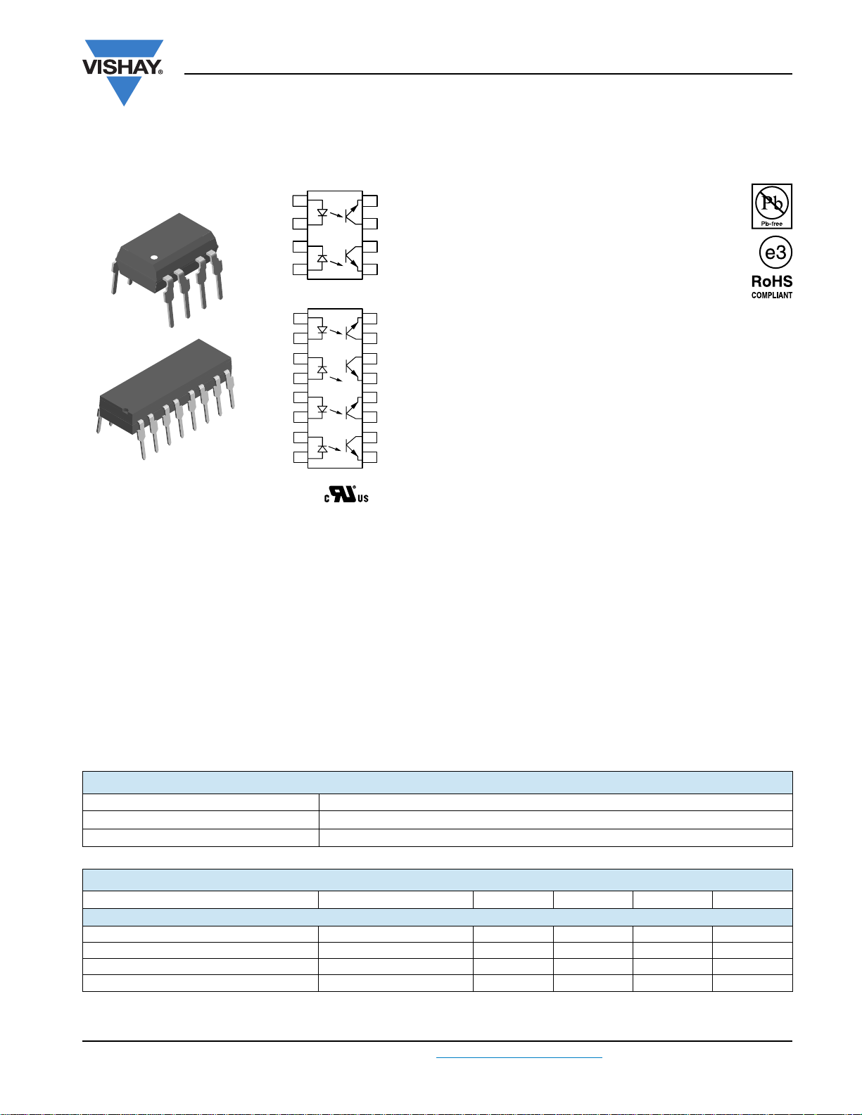
Optocoupler, Phototransistor Output (Multichannel)
Dual Channel
Quad Channel
i179015-1
A
C
C
A
A
C
C
A
A
C
C
A
i179015-2
1
2
3
4
1
2
3
4
5
6
7
8
8
E
7
C
C
6
E
5
16
E
15
C
C
14
13
E
12
E
C
11
C
10
E
9
DESCRIPTION
The CNY74-2H, CNY74-4H is an optically coupled pair with
a GaAIAs infrared LED and a silicon NPN phototransistor.
Signal information, including a DC level, can be transmitted
by the device while maintaining a high degree of electrical
isolation between input and output.
The CNY74-2H, CNY74-4H is especially for driving
medium-speed logic, where it may be used to eliminate
troublesome ground loop and noise problems. Also it can be
used to replace relays and transformers in many digital
interface applications, as well as analog applications such as
CTR modulation.
The CNY74-2H has two isolated channels in a single DIP
package; the CNY74-4H has four isolated channels per
package.
FEATURES
• CNY74-2H, CNY74-4H TTL compatible
• Transfer ratio, 35 % typical
• Coupling capacitance, 0.5 pF
• Dual and quad channel
• Industry standard DIP packages
• Compliant to RoHS directive 2002/95/EC and
in accordance to WEEE 2002/96/EC
AGENCY APPROVALS
• UL1577, file no. E52744 system code H, double protection
• UL1577, file no. E52744, equivalent to CSA bulletin 5A
ORDER INFORMATION
PART REMARKS
CNY74-2H CTR 50 % to 600 %, dual channel DIP-8
CNY74-4H CTR 50 % to 600 %, quad channel DIP-16
ABSOLUTE MAXIMUM RATINGS
PARAMETER TEST CONDITION PART SYMBOL VALUE UNIT
INPUT
Peak reverse voltage V
Forward continuous current I
Power dissipation P
R
F
diss
Derate linearly from 55 % 1.33 mW/°C
Document Number: 83526 For technical questions, contact: optocoupleranswers@vishay.com
Rev. 1.9, 20-Oct-09 1
3V
60 mA
100 mW
www.vishay.com
CNY74-2H, CNY74-4H
Vishay Semiconductors
Optocoupler, Phototransistor Output
(Multichannel)
ABSOLUTE MAXIMUM RATINGS
PARAMETER TEST CONDITION PART SYMBOL VALUE UNIT
OUTPUT
Collector emitter breakdown voltage BV
Emitter collector breakdown voltage BV
Power dissipation P
CEO
ECO
diss
Derate linearly from 25 °C 2mW/°C
COUPLER
Isolation test voltage t = 1 s V
V
Isolation resistance
Total package dissipation
Derate linearly from 25 °C
= 500 V, T
IO
V
= 500 V, T
IO
= 25 °C R
amb
= 100 °C R
amb
CNY74-2H P
CNY74-4H P
CNY74-2H 5.33 mW/°C
CNY74-4H 6.67 mW/°C
ISO
IO
IO
tot
tot
Creepage distance ≥ 7mm
Clearance distance ≥ 7mm
Storage temperature T
Operating temperature T
stg
amb
Lead soldering time at 260 °C 10 s
Note
T
= 25 °C, unless otherwise specified.
amb
Stresses in excess of the absolute maximum ratings can cause permanent damage to the device. Functional operation of the device is not implied
at these or any other conditions in excess of those given in the operational sections of this document. Exposure to absolute maximum ratings for
extended periods of the time can adversely affect reliability.
70 V
7V
150 mW
5300 V
12
≥ 10
11
≥ 10
RMS
Ω
Ω
400 mW
500 mW
- 55 to + 150 °C
- 55 to + 100 °C
ELECTRICAL CHARACTERISTICS
PARAMETER TEST CONDITION SYMBOL MIN. TYP. MAX. UNIT
INPUT
Forward voltage I
Reverse current V
Capacitance V
= 20 mA V
F
= 3 V I
R
= 0 V C
R
F
R
O
1.3 1.5 V
0.1 100 µA
25 pF
OUTPUT
Collector emitter breakdown voltage I
Collector emitter leakage current V
Capacitance collector emitter V
= 1 mA BV
C
= 5 V, IF = 0 A I
CE
= 0 V, f = 1 Hz C
CE
CEO
CEO
CE
70 V
100 nA
10 pF
COUPLER
Saturation voltage, collector emitter I
= 2 mA, IF = 16 mA V
C
Resistance (input to output) R
Capacitance (input to output) C
CEsat
IO
IO
0.3 0.5 V
100 GΩ
0.5 pF
Note
T
= 25 °C, unless otherwise specified.
amb
Minimum and maximum values are testing requirements. Typical values are characteristics of the device and are the result of engineering
evaluation. Typical values are for information only and are not part of the testing requirements.
CURRENT TRANSFER RATIO
PARAMETER TEST CONDITION SYMBOL MIN. TYP. MAX. UNIT
DC current transfer ratio I
DC current transfer ratio I
= 5 mA, VCE = 5 V CTR 50 600 %
F
= 10 mA, VCE = 5 V CTR 60 %
F
www.vishay.com For technical questions, contact: optocoupleranswers@vishay.com
Document Number: 83526
2 Rev. 1.9, 20-Oct-09
CNY74-2H, CNY74-4H
Optocoupler, Phototransistor Output
Vishay Semiconductors
(Multichannel)
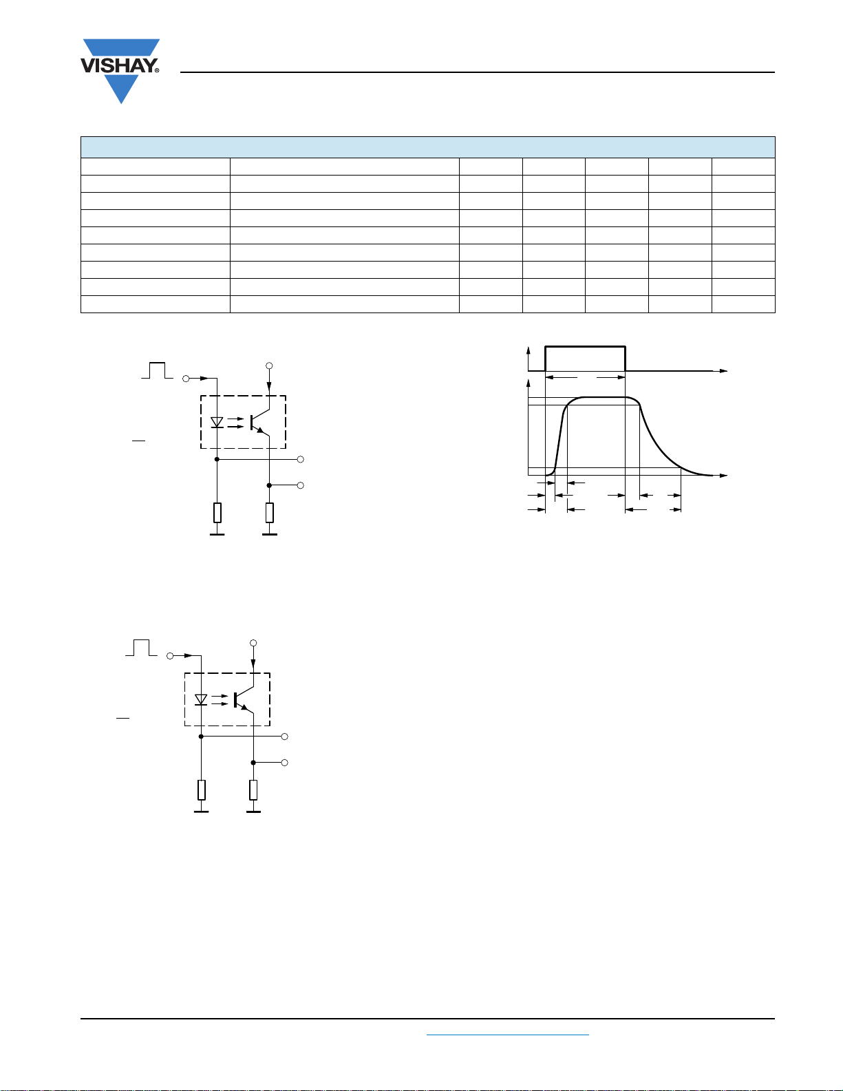
SWITCHING CHARACTERISTICS
PARAMETER TEST CONDITION SYMBOL MIN. TYP. MAX. UNIT
Delay time V
Rise time V
Fall time V
Storage time V
Turn-on time V
Turn-off time V
Turn-on time V
Turn-off time V
I
I
F
F
50 Ω 100 Ω
95 10804
0
RG = 50 Ω
t
p
= 0.01
T
tp = 50 µs
Fig. 1 - Test Circuit, Non-Saturated Operation
= 5 V, IC = 2 mA, RL = 100 Ω (see figure 1) t
S
= 5 V, IC = 2 mA, RL = 100 Ω (see figure 1) t
S
= 5 V, IC = 2 mA, RL = 100 Ω (see figure 1) t
S
= 5 V, IC = 2 mA, RL = 100 Ω (see figure 1) t
S
= 5 V, IC = 2 mA, RL = 100 Ω (see figure 1) t
S
= 5 V, IC = 2 mA, RL = 100 Ω (see figure 1) t
S
= 5 V, IC = 10 mA, RL = 1 kΩ (see figure 2) t
S
= 5 V, IC = 10 mA, RL = 1 kΩ (see figure 2) t
S
+ 5 V
IC = 2 mA; adjusted through
Channel I
Channel II
input amplitude
Oscilloscope
R
= 1 MΩ
L
= 20 pF
C
L
d
r
f
s
on
off
on
off
I
F
0
I
C
100 %
90 %
10 %
0
t
t
d
t
t
p
t
d
t
r
(= td + tr) Turn-on time
t
on
on
Pulse duration
Delay time
Rise time
Fig. 3 - Switching Times
3µs
3µs
4.7 µs
0.3 µs
6µs
5µs
9µs
18 µs
t
p
r
t
f
t
s
t
off
t
s
t
f
t
(= ts + tf)Turn-off time
off
t
t
Storage time
Fall time
96 11698
1 kΩ
+ 5 V
I
C
Channel I
Channel II
Oscilloscope
R
1 MΩ
≥
L
C
20 pF
≤
L
0
RG= 50 Ω
t
p
= 0.01
T
tp= 50 µs
95 10843
I
= 10 mA
I
F
F
50 Ω
Fig. 2 - Test Circuit, Saturated Operation
Document Number: 83526 For technical questions, contact: optocoupleranswers@vishay.com
www.vishay.com
Rev. 1.9, 20-Oct-09 3
 Loading...