

TELEFUNKEN BYW 76 TEL Datasheet
Fast Silicon Mesa Rectifiers
R
V
Re etitive eak reverse voltage
V
Junction ambient
R
K/W
Reverse current
I
A
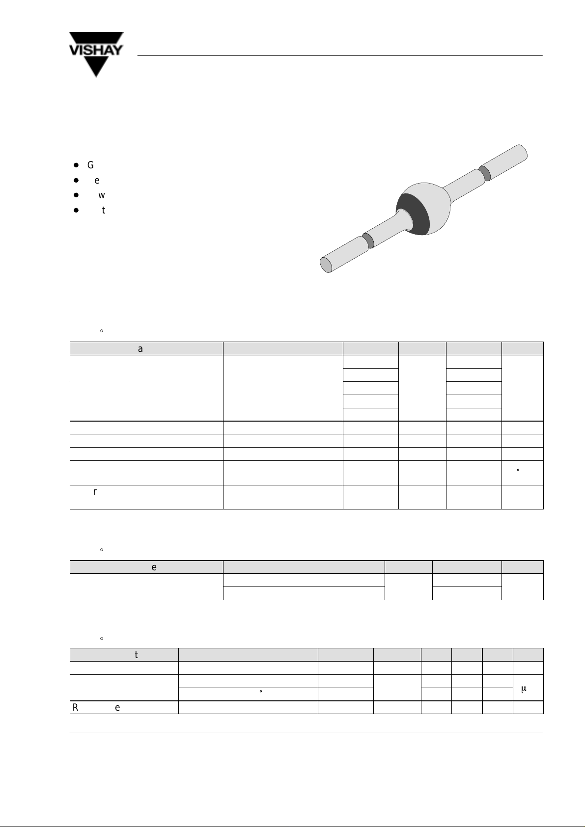
Features
D
Glass passivated junction
D
Hermetically sealed package
D
Low reverse current
D
Soft recovery characteristics
Applications
BYW72...BYW76
Vishay Telefunken
Fast rectifier and switch for example for TV–line output
circuits and switch mode power supply
Absolute Maximum Ratings
Tj = 25_C
Parameter Test Conditions Type Symbol Value Unit
BYW72 200
everse voltage=
p
Peak forward surge current tp=10ms, half sinewave I
Repetitive peak forward current I
Average forward current I
Junction and storage
temperature range
Non repetitive reverse
avalanche energy
p
I
=0.4A E
(BR)R
BYW73
BYW74
BYW75
BYW76 600
Maximum Thermal Resistance
Tj = 25_C
Parameter Test Conditions Symbol Value Unit
l=10mm, TL=constant
on PC board with spacing 25mm
Tj=T
thJA
R
RRM
FSM
FRM
FAV
R
=
stg
94 9588
300
400 V
500
100 A
15 A
3 A
–65...+175
10 mJ
25
70
°
C
Electrical Characteristics
Tj = 25_C
Parameter Test Conditions Type Symbol Min Typ Max Unit
Forward voltage IF=3A V
Reverse recovery time IF=0.5A, IR=1A, iR=0.25A t
Document Number 86050
Rev. 4, 27-Sep-00
VR=V
VR=V
RRM
, Tj=150°C
RRM
F
R
rr
0.95 1.1 V
1 5
60 150
200 ns
www.vishay.com
m
1 (4)
BYW72...BYW76
Vishay Telefunken
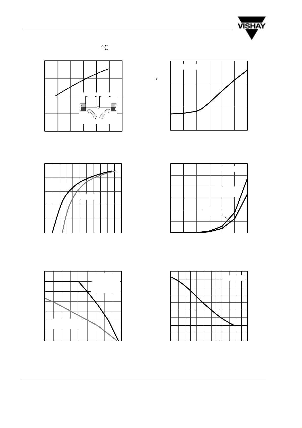
Characteristics (Tj = 25_C unless otherwise specified)
40
30
ll
TL=constant
20
30
thJA
R – Therm. Resist. Junction / Ambient ( K/W )
94 9548
20
10
0
0 5 10 15 25
l – Lead Length ( mm )
Figure 1. Max. Thermal Resistance vs. Lead Length
100.000
10.000
Tj=175°C
1.000
Tj=25°C
0.100
F
0.010
I – Forward Current ( A)
0.001
0 0.2 0.4 0.6 0.8 1.0 1.2 1.4 1.6 1.8 2.0 2.2
VF – Forward Voltage ( V )16355
1000
VR = V
RRM
m
100
10
R
I – Reverse Current ( A )
1
25 50 75 100 125 150 175
Tj – Junction Temperature ( °C )16357
Figure 4. Reverse Current vs. Junction Temperature
300
VR = V
RRM
250
200
150
100
50
R
P – Reverse Power Dissipation ( mW )
0
25 50 75 100 125 150 175
Tj – Junction Temperature ( °C )16358
PR–Limit
@80%V
PR–Limit
@100%V
R
R
Figure 2. Forward Current vs. Forward Voltage
Figure 5. Max. Reverse Power Dissipation vs.
Junction Temperature
3.5
3.0
2.5
2.0
1.5
1.0
0.5
FAV
I – Average Forward Current ( A )
R
=70K/W
thJA
PCB: d=25mm
0
0 20 40 60 80 100 120 140 160 180
T
– Ambient Temperature ( °C )16356
amb
VR=V
RRM
half sinewave
R
=45K/W
thJA
l=10mm
Figure 3. Max. Average Forward Current vs.
90
80
70
60
50
40
30
20
D
C – Diode Capacitance ( pF )
10
0
0.1 1.0 10.0 100.0
VR – Reverse Voltage ( V )16359
f=1MHz
Figure 6. Diode Capacitance vs. Reverse Voltage
Ambient Temperature
www.vishay.com Document Number 86050
2 (4) Rev. 4, 27-Sep-00
 Loading...