

Teledyne e2V EV71YC1CNT4005-BA0, EV71YC1CNT2010-BA0 User Manual
e2v.com/cameras
USER MANUAL
UNIIQA+ NBase-T COLOR

UM_UNIIQA+_NBASE-T_COLOUR REV.E 09/2018
P A G E | 2
Table of Contents
1 Camera Overview .................................................................................................................... 5
1.1 Features ......................................................................................................................................................... 5
1.2 Key Specifications .......................................................................................................................................... 5
1.3 Description..................................................................................................................................................... 6
1.4 Applications ................................................................................................................................................... 6
1.5 Models ........................................................................................................................................................... 6
2 Camera Performances ............................................................................................................. 7
2.1 Camera Characterization ............................................................................................................................... 7
2.2 Image Sensor and colour modes ................................................................................................................... 7
2.2.1 4k pixels 5x5µm (Full Definition) ............................................................................................................ 8
2.2.2 2k, 1k or 512 pixels 10x10µm (True Color) ............................................................................................. 8
2.3 Response & QE curves ................................................................................................................................. 10
2.3.1 Quantum Efficiency .............................................................................................................................. 10
2.3.2 Spectral Response ................................................................................................................................ 10
3 Camera Hardware Interface ................................................................................................... 11
3.1 Input/output Connectors and LED............................................................................................................... 12
3.2 Power Connector ......................................................................................................................................... 12
3.2.1 Status LED Behaviour ............................................................................................................................ 13
3.3 GPIO Connector ........................................................................................................................................... 13
4 STANDARD CONFORMITY ...................................................................................................... 15
4.1 CE Conformity .............................................................................................................................................. 15
4.2 FCC Conformity ............................................................................................................................................ 15
4.3 RoHs Conformity .......................................................................................................................................... 15
5 Camera Interface : NBASE-TTM ............................................................................................... 16
5.1 What is the NBASE-TTM Technology ? .......................................................................................................... 16
6 Camera Interface Overview ................................................................................................... 17
6.1 Inputs, Outputs and Enhanced Features ..................................................................................................... 17
7 Camera Commands ............................................................................................................... 19
7.1 Device Control ............................................................................................................................................. 19
7.2 Image Format Control ................................................................................................................................. 20
7.2.1 Image Format ....................................................................................................................................... 20
7.2.2 Meta Data ............................................................................................................................................. 20

UM_UNIIQA+_NBASE-T_COLOUR REV.E 09/2018
P A G E | 3
7.2.3 Regions of Interest ................................................................................................................................ 21
7.3 Transport Layer Control ............................................................................................................................... 23
7.4 Acquisition Control ...................................................................................................................................... 26
7.4.1 GenICam Triggers ................................................................................................................................. 26
7.4.2 Cycling Preset modes and configuration .............................................................................................. 30
7.5 Digital I/O Control ........................................................................................................................................ 32
7.6 Enhanced Features Control ......................................................................................................................... 37
7.6.1 Rotary Encoder, Rescaler and Frame Delay.......................................................................................... 37
7.6.2 Counters & Timers ................................................................................................................................ 39
7.7 Gain Control ................................................................................................................................................. 46
7.8 Flat Field Correction Control ....................................................................................................................... 48
7.8.1 FFC Calibration and Bank/Preset Saving ............................................................................................... 48
7.8.2 PRNU Low Frequency Filter for FFC ...................................................................................................... 50
7.9 Color Management Control ......................................................................................................................... 52
7.9.1 White Balance ....................................................................................................................................... 52
7.9.2 RGB Color Matrix .................................................................................................................................. 52
7.10 Device Access Control ................................................................................................................................ 57
7.11 Save and Restore ....................................................................................................................................... 57
APPENDIX ................................................................................................................................ 59
Appendix A. Pattern Tests ........................................................................................................ 60
A.1 Test Pattern 1: Vertical wave ...................................................................................................................... 60
A.2 Test Pattern 2: Fixed Horizontal Ramps ...................................................................................................... 60
Appendix B. Timing Diagrams ................................................................................................... 61
B.1 Synchronization modes with variable Exposure Time ................................................................................ 61
B.2 Synchronization modes with Fixed Exposure Time ..................................................................................... 62
B.3 Timing Values .............................................................................................................................................. 62
Appendix C. Accessories ........................................................................................................... 63
C.1 F-Mount ....................................................................................................................................................... 63
C.2 C-Mount ....................................................................................................................................................... 64
C.3 Set of Heatsinks ........................................................................................................................................... 65
Appendix D. Network Connection ............................................................................................. 66
D.1 Single Network Board + Cables (GPIO + Power) Kit .................................................................................... 66
D.2 Dual Network Board + Cables (GPIO + Power) Kit ...................................................................................... 66
D.3 Ethernet Cable............................................................................................................................................. 66
D.4 PureGev Application and eBus Package ...................................................................................................... 67

UM_UNIIQA+_NBASE-T_COLOUR REV.E 09/2018
P A G E | 4
D.5 Driver Configuration and Inter-Operablity .................................................................................................. 67
Appendix E. Revision History .................................................................................................... 68

UM_UNIIQA+_NBASE-T_COLOUR REV.E 09/2018
P A G E | 5
1 Camera Overview
1.1 Features
Cmos Colour Sensor :
4096 RGB Pixels 5x5µm (Full Definition)
2048 RGB Pixels 10x10µm (True Colour)
Interface : NBASE-T™ (up to 5Gb/s)
Line Rate :
50 000 l/s In 4k Full Definition Mode
100 000 l/s in 2k True Colour Mode
Bit Depth : 24bits (RGB 8bits)
Scan Direction
Flat Field Correction
Cycling Preset Modes and Memories
Multi ROI
Metadata
Rotary Encoder
1.2 Key Specifications
Characteristics
Typical Value
Unit
Sensor Characteristics at Maximum Pixel Rate
Resolution
4096 2048
RGB Pixels
pixel size (square)
5 10
µm
Max Line Rate
50 100
kHz
Radiometric Performance at Maximum Pixel Rate and minimum camera gain
Bit depth
3 x 8
Bits
Response non linearity
< 1
%
PRNU HF Max 3 %
Dynamic range
65
dB
Peak Response (All Modes)
Red
11.8
LSB 8bits/(nJ/cm²)
Green
11.2
LSB 8bits/(nJ/cm²)
Blue
7.8
LSB 8bits/(nJ/cm²)
Test conditions :
All values are given at Nominal Gain (0dB) : Preamp Gain x1, Amp Gain 0dB
Figures in LSB are for a 8bits format
Measured at exposure time = 400µs and line period = 400µs in Ext Trig Mode (Max Exposure Time)
Maximum data rate

UM_UNIIQA+_NBASE-T_COLOUR REV.E 09/2018
P A G E | 6
1.3 Description
To maintain their competitive advantage, industrial leaders in the machine vision market have a continuous
requirement to improve defect detection accuracy and reduce the cost of imaging. The availability of the
UNIIQA+ cameras with an NBASE-T™ connection offers a straightforward solution, providing:
High throughput - enabling high resolution and colour imaging without a frame grabber at speeds of up to
5 Gigabits per second (Gbps) over Category 5e standard Ethernet cable.
Easy integration – compatible with GigE Vision protocol.
Long-length (100 meters+), field terminable, inexpensive cabling - reduces costs and enables easier
integration in imaging systems compared with optic fibre cabling
1.4 Applications
Raw material surface inspection
Parcel and postal sorting
High resolution document scanning
Printing inspection
Industrial Inspection
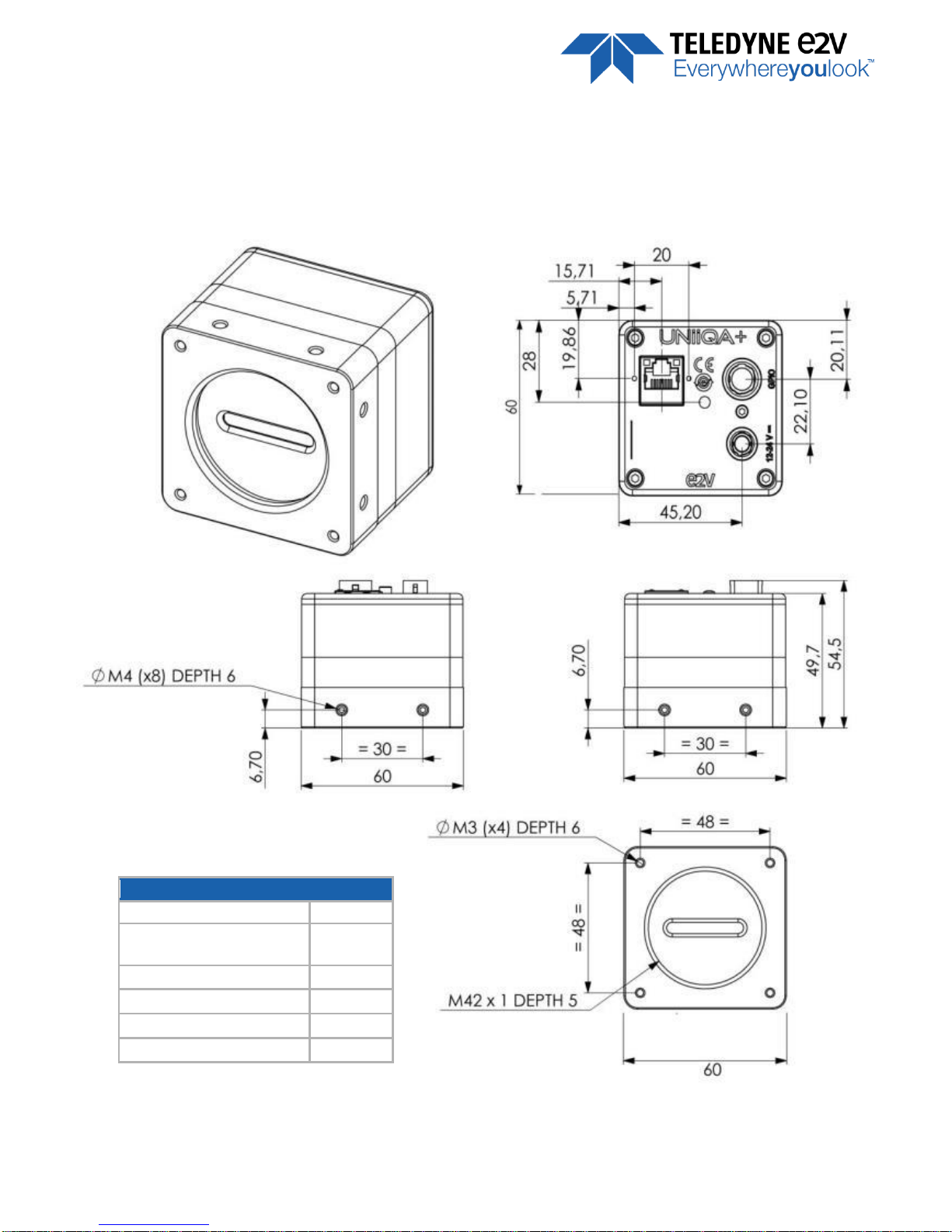
1.5 Models
Functionality (Programmable via GenICam Control Interface)
Analog Gain
Up to 12 (x4)
dB
Trigger Mode
Timed (Free run) and triggered (Ext Trig, Ext ITC) modes
Sensor Modes
True Colour Single : 2048 RGB Pixels of 10x10µm
Full Definition Single : 4096 RGB Pixels 5x5µm
Mechanical and Electrical Interface
Size (w x h x l)
60 x 60 x 55
mm
Weight
247/335 without/with Heat Sinks
g
Lens Mounts
C, F, T2, M42 (embedded in the Front Face)
-
Sensor alignment
±100
µm
Sensor flatness
±50
µm
Power supply
12 - 24
V
Power dissipation
< 11
W
General Features
Operating temperature
0 to 60 (front face) or 85 (Internal)
°C
Storage temperature
-40 to 70
°C
Regulatory
CE, FCC and RoHS compliant
Part Number
Definition
Max Speed
Details
EV71YC1CNT4005-BA0
4k x 5µm
50kHz
Delivered with a pair of Heat Sinks
EV71YC1CNT2010-BA0
2k x 10µm
100kHz
UM_UNIIQA+_NBASE-T_COLOUR REV.E 09/2018
P A G E | 7
2 Camera Performances
2.1 Camera Characterization
Unit
4k 5µm or 2k 10µm Single
Typ.
Max
Dark Noise RMS
LSB
0.45
0.8
Dynamic Range
db
53
-
RMS Noise (3/4 Sat)
LSB
2.15
4
Full Well Capacity
e- (per color)
22000
-
SNR (3/4 Sat)
dB
42
-
Peak Response (460/530/660nm)
LSB 8bits/
(nJ/cm2)
4/5/6
-
Non Linearity
%
0,3
-
Without Flat Field Correction :
FPN rms
LSB
0.15
0.5
FPN pk-pk
LSB
0.85
2
PRNU hf (3/4 Sat)
%
0.24
0,5
PRNU pk-pk (3/4 Sat)
%
1.7
3
All LSB Values are in 8bits (RGB : 3x8bits) at nominal Gain
2.2 Image Sensor and colour modes
The Uniiqa+ sensor is composed of two sensitive lines of 4096 pixels of 5µm square : One composed of Green
pixels only, the second one composed alternatively of Red/Blue Pixels.
Each pixel on the same column uses its own Analog to Digital Column converter (ADC Column).
This structure allows several definitions :
4k pixels 5x5µm (Full Definition) :
The 2 color lines are exposed with a delay of
one line in order to match the same position
between the green line and the red/blue line
2k Pixels 10x10µm (True Color) :
The colored pixel is composed of 2x Green
pixels, one red and one blue exposed in the
same time.
Then, 1k or 0,5k 10x10µm are achieved by
applying an ROI on the centre of the sensor
from the 2k 10x10µm
4096 Pixels 5x5µm
Memory Node
ADC Column
Memory Node
Pixel Line A
Pixel Line B
ADC Column
UM_UNIIQA+_NBASE-T_COLOUR REV.E 09/2018
P A G E | 8
2.2.1 4k pixels 5x5µm (Full Definition)
This color mode (5µm) requires the indication of “Forward/Reverse” to the camera in order to manage the
delay between the two colored lines.
2.2.2 2k, 1k or 512 pixels 10x10µm (True Color)
These color modes don’t require any Reverse/Forward indication if no interpolation is used (or only the
”column interpolation”)
Column Interpolation Correction
This interpolation is used to compensate the colour error in the Red or the Blue in case of a
vertical transition on the web : The Red of the blue value of each coloured pixel is corrected
if the variation between two neighbour green pixels is significant.
B1’ = αB x B
1
and αB is the blue correction, calculated with the variation (G1–G2)
R2’ = αR x R
2
and αR is the red correction, calculated with the variation (G1–G2)
This interpolation is available only for pixel size 10x10µm (True Colour only)
It can be disabled by the customer. By default, it is enabled.
Line Interpolation Correction
This interpolation is used to compensate the colour error in the Red
or the Blue in case of a horizontal transition on the web in the same
“True Colour” pixel : A line is memorized and the Red of the blue
value of each coloured pixel is corrected if the variation between
two consecutive green values (previous to next line) is significant :
B1’ = αB x B
1
and αB is the blue correction, calculated with the
variation (G1–G’1)
R2’ = αR x R
2
and αR is the red correction, calculated with the
variation (G2–G’2)
G1
G2
B1
R2
Vertical
G1
G2
B1
R2
G’1
G’
B’1
R’2
Two consecutive
Horizontal
Previous
delay
5µm
5µm
G1
G2
G3
G4
B1
R2
B3
R4
Web
direction
R2
G1
B1
R2
G2
B1+B3
2
R2+R4
2
G3
B3
R4
G4
B3+B5
2
10µm
10µm
G1
G2
G3
G4
B1
R2
B3
R4
Web
direction
R2
(G1+ G2)/2
B1
R4
(G3+ G4)/2
B3
No interpolation
UM_UNIIQA+_NBASE-T_COLOUR REV.E 09/2018
P A G E | 9
This interpolation is available only for pixel size 10x10µm (True Colour Single only)
It can be enabled by the customer. By default, it is disabled
This interpolation requires the Forward/Reverse indication sent to the camera for the memorized line.
The Line Interpolation has to be disabled if the light is changing for each Line (typically for
pulsed Light source with different spectrum) or for any reason the Green component of
the light source changes significantly from one line to the next one.
Effects of the interpolation corrections
Horizontal transition effect reduced by the “Line Interpolation”
Vertical transition effect reduced by the “Column Interpolation”
Color Interpolation in Full Definition modes.
This colour mode (5µm) requires the indication of “Forward/Reverse” to the camera in order to manage the
delay between the two coloured lines.
delay
5µm
5µm
G1
G2
G3
G4
B1
R2
B3
R4
Web
direction
R2
G1
B1
R2
G2
B1+B3
2
R2+R4
2
G3
B3
R4
G4
B3+B5
2
Magenta color ghosting
Green color ghosting
Red color
ghosting
Blue
color
ghosting
After both
column and Line
Interpolations
UM_UNIIQA+_NBASE-T_COLOUR REV.E 09/2018
P A G E | 10
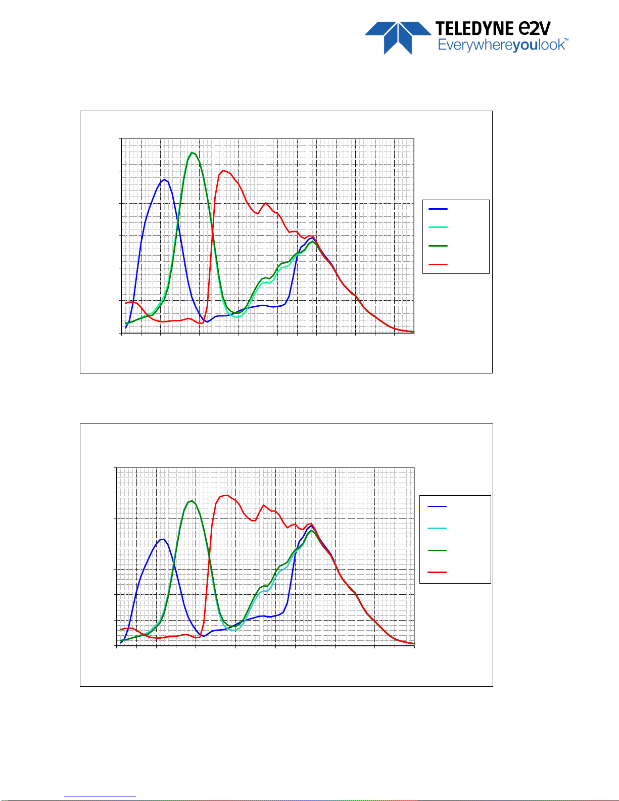
2.3 Response & QE curves
2.3.1 Quantum Efficiency
2.3.2 Spectral Response
0%
10%
20%
30%
40%
50%
60%
350 400 450 500 550 600 650 700 750 800 850 900 950 1000 1050 1100
Wavelength (nm)
Quantum Efficiency
Blue
Green blue
Green red
Red
0
1
2
3
4
5
6
7
350 400 450 500 550 600 650 700 750 800 850 900 950 1000 1050 1100
(LSB 8-bit/(nJ/cm²))
Wavelength (nm)
Spectral response (Single Modes)
Blue
Green blue
Green red
Red
UM_UNIIQA+_NBASE-T_COLOUR REV.E 09/2018
P A G E | 11
3 Camera Hardware Interface
Sensor alignment
Z = -10.3 mm
±100µm
X = 19.76 mm (4k 5µm)
X = 19.76 mm (2k 10µm)
±100 µm
Y = 30 mm
±100 µm
Die flatness
50 µm
Rotation (X,Y plan)
±0.3°
Parallelism
50µm
UM_UNIIQA+_NBASE-T_COLOUR REV.E 09/2018
P A G E | 12
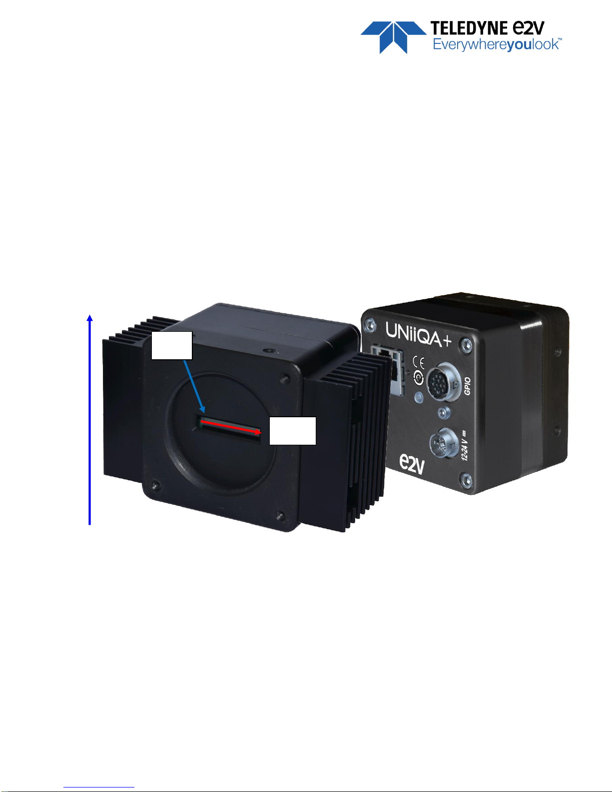
3.1 Input/output Connectors and LED
3.2 Power Connector
Camera connector type: Hirose HR10A-7R-6PB (male)
Cable connector type: Hirose HR10A-7P-6S (female)
Camera side description
Signal
Pin
Signal
Pin
PWR
1
GND 4 PWR
2
GND 5 PWR
3
GND
6
Power supply from 12 to 24V
Power 11W max with an almost no inrush current peak
First 90ms after Power Up : The
maximum peak is about 90mA
90mA
Power
Connector :
12-24V DC
Multi-Coloured
LED for Status
Ethernet
RJ45 Connector
with Traffic &
Connection LED
GPIO
Connector
UM_UNIIQA+_NBASE-T_COLOUR REV.E 09/2018
P A G E | 13
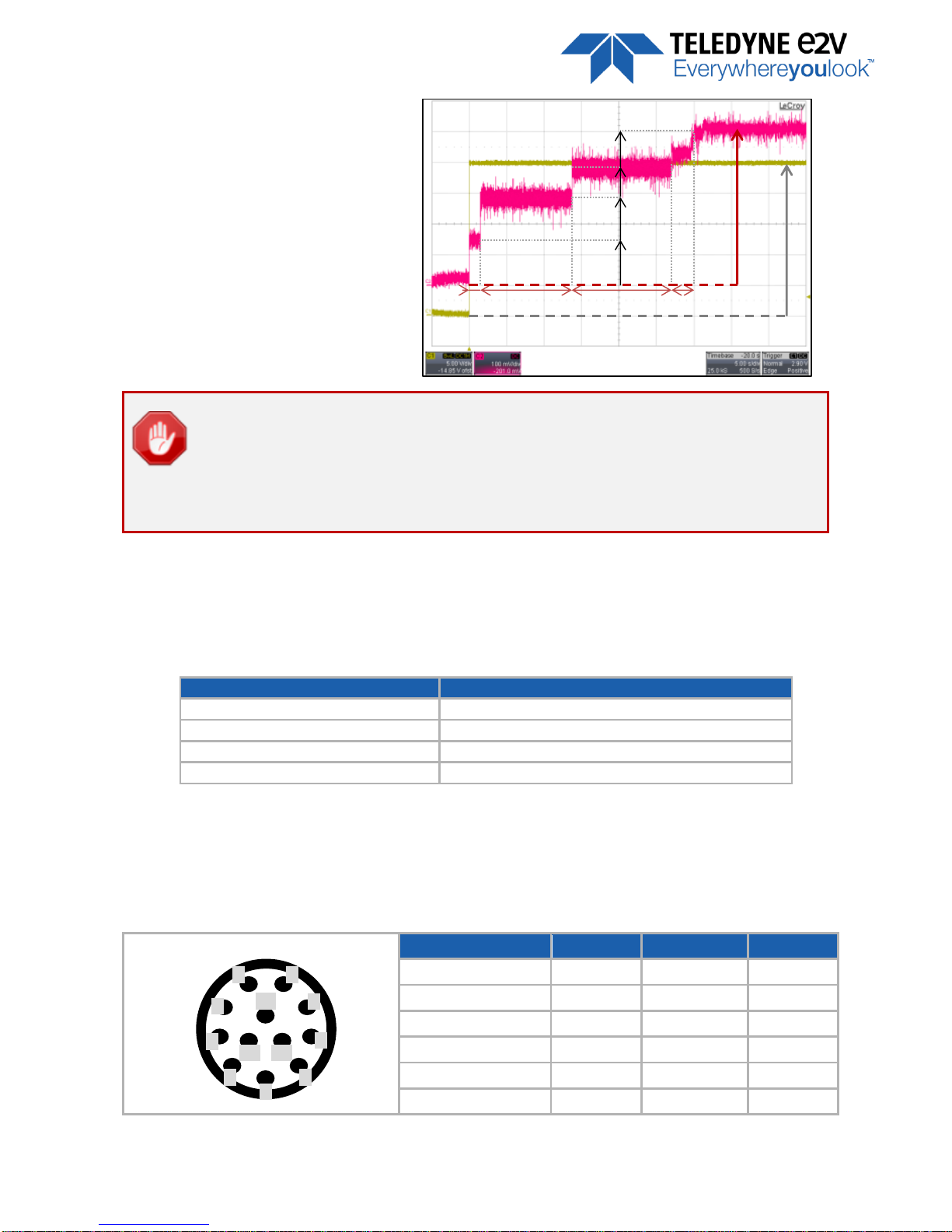
The complete Boot sequence :
No real peak of Inrush current
Several steps up to the nominal current
(about 430mA under 24V)
If the NIC Board (on PC Side) is not forced at 5Gb/s (no Auto-Negotiation or 10Gb/s) then a
peak of 1,5A can be observed at the boot on the camera power Supply. The 10Gb/s
connection is required only if you want achieve the real 5Gb/s (50kHz in 4k) otherwise you
can force the connection at 5Gb/s : This could prevent the camera to complete a safe boot
(depending on the Power provided)
3.2.1 Status LED Behaviour
After less than 2 seconds of power establishment, the LED first lights up in WHITE. Then after a Maximum of 40
seconds, the LED must turn in a following colour :
Colour and state
Meaning
Green
and continuous
OK
Green
and blinking slowly
Waiting for Ext Trig (Trig1 and/or Trig2)
Red
and continuous
Camera out of order : Internal firmware error
Blue
and continuous
Recovery (Upgrade mode) or Start boot sequence
3.3 GPIO Connector
Camera Connector type: Hirose HR10A-10R-12SB
Cable Connector type: Hirose HR10A-10R-12P
Cable type: cable immune from interference and with twisted pairs
Camera side description
Signal
Pin
Signal
Pin
Line 0+
1
Line 3+ 7 Line 0-
2
Line 4+ 8 Line 1+
3
Line 5+ 9 Line 1-
4
Line 6+
10
Line 2+
5
GND
11
Line 2-
6
GND
12
9
8 7 6
5
4 3 2
1
10
12
11
1.5
430m
2.9s
13.2
12.1
120mA
110mA
90mA
110mA
UM_UNIIQA+_NBASE-T_COLOUR REV.E 09/2018
P A G E | 14
Lines 0, 1 and 2
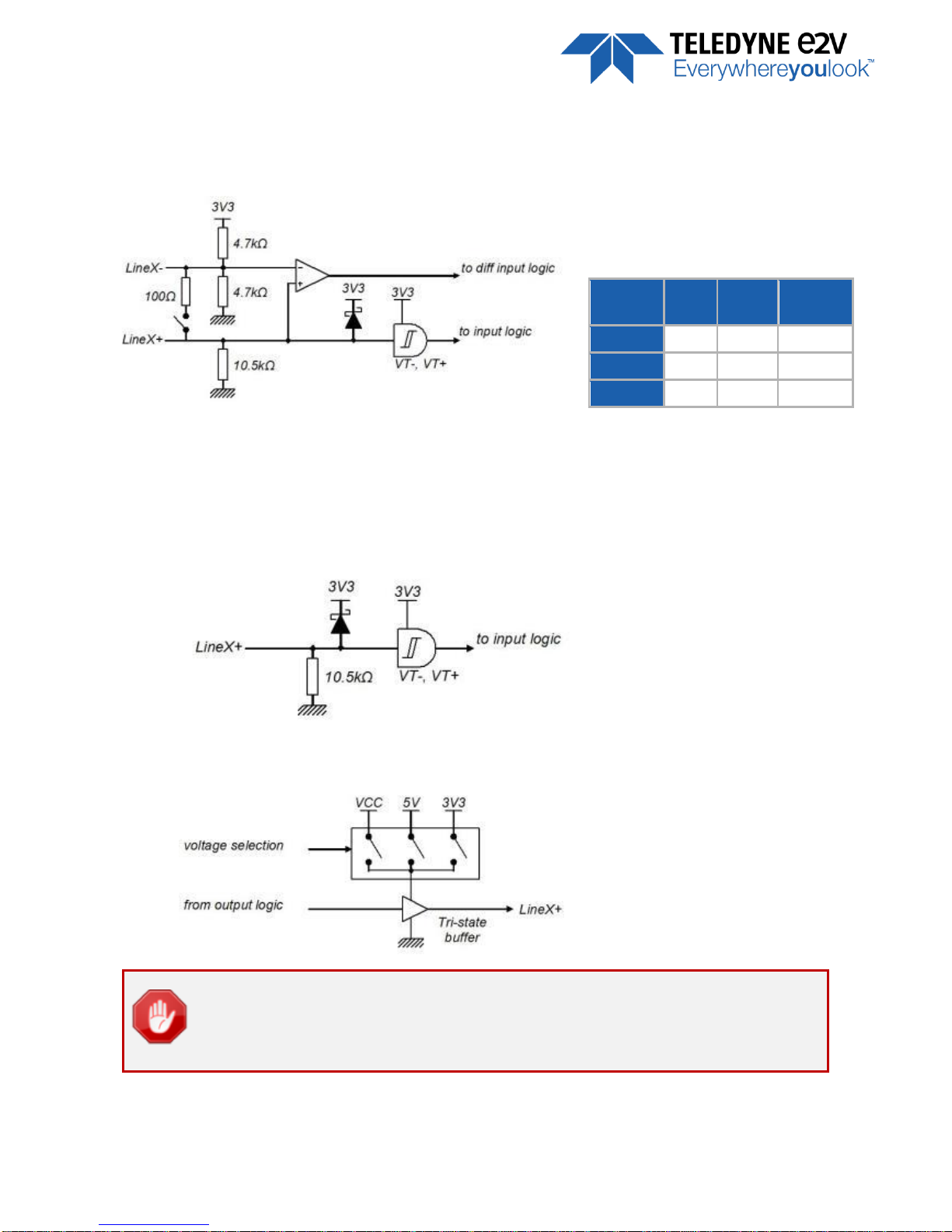
The GPIO Connector allows the following connections :
Line 0, 1 or 2
: Dedicated inputs for Line Triggers and Frame Trigger. Differential (RS422 with or without
termination) or TTL (Single End) in 3.3V, 5V, 12V or 24V.
Lines 3, 4, 5 and 6
Line 3, 4, 5 and 6
: Configurable Inputs or Outputs in TTL only :
Input Configuration : Single End in 3.3V, 5V, 12V or 24V
Output configuration : Single End or Open Collector in 3.3V, 5V, or Camera power Supply
INPUT Configuration
OUTPUT Configuration
Output Lines have a limited current of 100mA : You have to make sure that each output is
connected on sufficient resistance (depending on the output voltage) to avoid an over
current which could damage the output circuit.
Input
Thresholds
VT-
Min
VT+
Max
Unit
24V
5.5
10.7
V
12V
2.1
5.5
V
3.3 / 5V
0.5 2 V
(Principle Schematic)
(Principle Schematic)
(Principle Schematic)

UM_UNIIQA+_NBASE-T_COLOUR REV.E 09/2018
P A G E | 15
4 STANDARD CONFORMITY
The UNIIQA+ cameras have been tested using the following equipment:
A shielded power supply cable
A GigE cat 5E data transfer cable ref.
e2v recommends using the same configuration to ensure the compliance with the following standards.
4.1 CE Conformity
The UNIIQA+ cameras comply with the requirements of the EMC (European) directive
2004/108/EC (EN50081-2, EN 61000-6-2).
4.2 FCC Conformity
The UNIIQA+ cameras further comply with Part 15 of the FCC rules, which states that: Operation is subject to
the following two conditions:
This device may not cause harmful interference (EN55032), and
This device must accept any interference received, including interference that may cause undesired
operation (EN55024)
This equipment has been tested and found to comply with the limits for Class A digital device, pursuant to part
15 of the FCC rules. These limits are designed to provide reasonable protection against harmful interference
when the equipment is operated in a commercial environment. This equipment generates, uses and can radiate
radio frequency energy and, if not installed and used in accordance with the
instruction manual, may cause harmful interference to radio communications. Operation of this equipment in a
residential area is likely to cause harmful interference in which case the user will be required to correct the
interference at his own expense.
Warning: Changes or modifications to this unit not expressly approved by the party responsible for compliance
could void the user's authority to operate this equipment.
4.3 RoHs Conformity
UNIIQA+ cameras comply with the requirements of the RoHS directive 2011/65/EU.
UM_UNIIQA+_NBASE-T_COLOUR REV.E 09/2018
P A G E | 16
5 Camera Interface : NBASE-T
TM
5.1 What is the NBASE-T
TM
Technology ?
NBASE-T™ technology defines a new type of Ethernet signaling that boosts the speed of installed based
twisted-pair cabling well beyond the cable’s designed limit of 1 Gigabit per second (Gbps) for distances up to
100 meters.
Capable of reaching 2.5 and 5 Gbps using the large installed base of Cat5e and Cat6 cabling, NBASE-T™
solutions enable users to accelerate their networks in the most cost-effective, least disruptive manner.
Flexible silicon solutions can auto-negotiate the optimal network speed, be it the new NBASE-T™ rates, slower
2.5 Gbps and 5 Gbps rates and even 10Gbps for very high speed networks.
To introduce these new cameras, e2v has partnered with PLEORA
Technologies, the world’s leading supplier of high-performance video
interfaces, the first company from the machine vision industry to join the
NBASE-T™ Alliance, a consortium collaborating on new technologies that
extend the bandwidth capabilities of twisted-pair copper cabling using
standard Ethernet technology.
Then all NBASE-T™ UNIIQA+ are licensed for Pleora eBus SDK and PureGeV Software that you can download on
Pleora website (http://www.pleora.com/our-products/ebus-sdk)
The UNIIQA+ NBASE-T™ Camera is not compliant with a standard 1 Gbps NIC Board : You
need a 5/10Gbps Board (as the N-420 PCIe that can be delivered in option).
The following recommendations have to be taken in account for the configuration of the
Board in order to achieve optimal performances :
If you don’t need to reach the Highest speed (5Gbps), you can fix the Board speed
connection to 5Gbps (instead of Auto-Negociation) : This will avoid a significant peak of
current of 1.5A at the Power Up.
To reach the maximum throughput (5 Gbps which is equivalent to 50kHz in 4k pixels):
Update NIC driver (at least 4.4.405.152)
NIC board configuration:
> 10Gb/s connection
> Packet Size at 8192
> Enable Jumbo packet
> Number of RX Descriptors : 1000 (maximum)
> Number of TX Descriptor : 1000 (maximum)
UM_UNIIQA+_NBASE-T_COLOUR REV.E 09/2018
P A G E | 17
6 Camera Interface Overview
6.1 Inputs, Outputs and Enhanced Features
The Digital I/O Module allows the connection of 7 external Lines :
3 dedicated inputs (Line 0, 1 and 2) that can generate 2 Line Triggers (LT1 and LT2) and one Frame
Trigger (FT) that will be used as inputs in the Enhanced features Block.
4 convertible generic Inputs / Outputs (Line 3, 4, 5 and 6) that can generate up to 4 additional Input
Lines (L3, 4, 5 and 6) that will be used also in the Enhanced features Block or Used as Outputs.
A flexible in/Out block in RS422 or TTL with different detection levels (3.3v, 5v, 12v, 24v)
A Debounce and Inverter block that can filter and invert the internal Signals Inputs once affected to
LT1, LT2, FT, L3, L4, L5 or L6.
The Enhanced Feature block completes the treatment on internal signals to generate Triggers :
A delay dedicated to the Frame Trigger only (FT)
A Full Rotary Encoder management (Quadratic with or without reverse miscount) that use by default
LT1 and LT2 as A/B Inputs. It can be bypassed to output by default LT1 as single Line Trigger input.
A Rescaler following the Rotary Encoder module (available also if Rotary Encoder is bypassed)
2x Counters and 2x Timers
The Internal Signals provided by the Digital I/O Block and the Enhance Feature block are :
LT1/2 : Line Trigger 1/2
RO : Rotary Encoder Output
FT : Frame Trigger (Signal Issued from the DigitalIOControl Block)
Frame Valid (Signal issued from the Frame Valid GenICam Trigger)
Frame Start (Signal issued from the Frame Start GenICam Trigger)
FLO (Exposure Active in the Sensor)
Lx : Line Inputs (L3, L4, L5, L6)
TE1/2 : Timers End 1/2
CE1/2 : Counters End 1/2
Then these Signals will be used to generate the 4 possible GenICam Triggers :
Line Start : With Exposure mode Off or Timed and a possible Delay before Exposure.
Exposure Active : With Exposure mode in TriggerWidth, linked to the Trigger signal level
Frame Start : The Frame Length is fixed and set by “Height” parameter.
Frame Active : For a variable Frame Length which depends on the Frame Trigger
Some other Interesting Features :
Delay
Rotary
Encoder
Rescaler
Debounce
And
Inverter
Line 0
Line 1
Line 2
Line 3
Line 4
Line 5
Line 6
3.3v
5v
12v
24v
RS422
TTL
Outputs :
-Software
-Pulse on internal event
-Cycling Preset active
Line Trigger 1 (LT1)
Line Trigger 2 (LT2)
Frame Trigger (FT)
Triggers
and
Inputs
2 x Counters
2 x Timers
FT
RO
Lx
TE
CE
Digital I/O Control
Enhanced Features

UM_UNIIQA+_NBASE-T_COLOUR REV.E 09/2018
P A G E | 18
A cycling mode which allows looping over a sequence of up to 8 Steps the 4 Possible Presets of
Parameters (Gain, Exposure Time and Delay, FFC, White Balance, Colour Correction Matrix …)
Up to 4x Region of Interests with separate FFC can be selected for Output
Additional Metadata at the end of each Line : Current Exposure Time, Missed Trigger, Current Preset,
TimeStamp, Line Counter, Timers and Counters values …

UM_UNIIQA+_NBASE-T_COLOUR REV.E 09/2018
P A G E | 19
7 Camera Commands
7.1 Device Control
GenCP address
GenICam Register
Size
(Bytes)
R/W
Description
0x00011030
DeviceScanType
4
RO
AreaScan (0) or LineScan (1)
0x0048
DeviceVendorName
32
RO
e2v
0x0068
DeviceModelName
32
RO
NBASE_T_COLOUR
0x00A8
DeviceManufacturerInfo
48
RO
Camera Part Number : EV71C1CNTxxxx-BA0
0x0088
DeviceVersion
32
RO
Camera Firmware Version
0x00D8
DeviceSerialNumber
16
RO
Camera Serial Number : YYWWAxxxx
0x00E8
DeviceUserID
16
RW
Camera ID set by the User
0x11088
DeviceSFNCVersionMajor
4
RO
2
0x1108C
DeviceSFNCVersionMinor
4
RO
0
0x11090
DeviceSFNCVersionSubMinor
4
RO
0
-
DeviceTLVersionMajor
4
RO
2 (mapped on GevVersionMajor)
-
DeviceTLVersionMinor
4
RO
0 (mapped on GevVersionMinor)
-
DeviceLinkSelector
4
RO
1
DeviceLinkSpeed
4
RO
625000000
-
DeviceLinkHeartbeatTimeout
4
RW
(5s by default)
DeviceLinkCommandTimeout
4
RW
(1s by default)
0x0904
DeviceStreamChannelCount
4
RO
1
DeviceStreamChannelType
4
RO
Transmitter (0), Receiver (1)
DeviceStreamChannelEndianness
4
RW
Big (0), Little (1)
DeviceStreamChannelPacketSize
4
RW
-
0x0900
DeviceEventChannelCount
4
RO
1
DeviceCharacterSet
4
RO
ASCII(0), UFT8(1)
DeviceRegistersEndianness
4
RO
Big(0), Little(1)
0x4E058098
CameraTemperature
4
RO
Read temperature value of the Device
Format : Q10.2 in degree Celsius (-511/512)
0x4E058078
ElectronicBoardID
32
RO
Production info
0x4E05809C
ElectronicBoardTestStatus
32
RO
Production info
0x4E058114
Reboot
4
WO
Command : Set to 1 to reboot the Camera
-
TimeStampReset
4
WO
Command to Reset the TimeStamp
-
TimestampLatch
4
W0
Command to latch the TimeStamp with Custom Value
-
TimestampLatchValue
32
RW
Value to latch the TimeStamp on Command
0x4E060608
ManufacturerIndex
8
RO
Index of production set in Factory
0x4E058110
Status
4
RO
Camera Status :
Bit0 to 7 : Reserved
Bit8 : Overflow occurs during FFC calibration
Bit9 : Underflow occurs during FFC calibration
Bit10 : Calibration Error
Bit11 : Scan Direction (Forward : 0, Reverse : 1)
Bit12 : Reserved
Bit14 : Initialization error
Bit13 : Reserved
Bit15 : Hardware error detected during init
0x4E060644
MissedTriggerCount
4
RO
Missed Triggers Internal Counter
UM_UNIIQA+_NBASE-T_COLOUR REV.E 09/2018
P A G E | 20
7.2 Image Format Control
This section includes all the settings relative to the Image Format and size.
7.2.1 Image Format
Height : Set the Height of the Image, but also the Buffer’s Heights in the Application. From 1 to 16383
Test Image Selector : Test Patterns are defined in Appendix A
Reverse Reading : Reverse output the line in the “X” Direction.
Sensor Mode : Depends on the camera Sensor version : Full Definition for 4k and True Color for 2k.
Scan Direction : Defines the if the Standard web direction is forward or Reverse versus the Mounting of
the camera in the System. If Set on External, it is defined by the Scan Direction Source Signal (0:Forward,
1:Reverse) :
The Scan direction information is available and useful only for the 4k version as green and Blue/Red Lines
information are grabbed separately and then the grabbing direction makes sense.
7.2.2 Meta Data
When enabled, Meta Data are added at the End of Each Line for a total of 24 Bytes (Equivalent of 8 RGB Pixels.
In the table below :
M0/M1/M2 are the R/G/B components of the First Pixel
…
M21/M22/M23 are the R/G/B components of the 8th Pixel
FORWARD
Web
Direction
Readout
order
First
Pixel

UM_UNIIQA+_NBASE-T_COLOUR REV.E 09/2018
P A G E | 21
7.2.3 Regions of Interest
Up to 4 Regions of Interest can be set :
No Overlap is possible between the different ROI : Start and width defined for each ROI.
Each ROI will perform its own Flat Field Correction (Max reference taken in the ROI).
Example with 3 ROI on a “Film Scanning” Image :
Original Image ROIs Definition Outputted Image
Pixel n°
Component
Data
Name
Details
1
R = M0
[7:0]
Exposure Time
Value on 2 Bytes.
Multiple of 100ns from 0 to 6553,5µs
G = M1
[15:8]
B = M2
[23:16]
Missed Trigger
Bit2 (D18) set to 1. Reset by Register
2
R = M3
[31:24]
Current Cycling Preset
Bit(1:0) : Value of the cycling Preset in Use
G = M4
[39:32]
Line Counter Value
Line Number (Counter). Reset by register.
Integer value on 4 Bytes : 0 to 232-1
B = M5
[47:40]
3
R = M6
[55:48]
G = M7
[63:56]
B = M8
[71:64]
Counter 1 Value
16 LSB of the Counter 1 Value
4
R = M9
[79:72]
G = M10
[87:80]
Counter 2 Value
16 LSB of the Counter 2 Value
B = M11
[95:88]
5
R = M12
[103:96]
Timer 1 Value
16 LSB of the Timer 1 Value
G = M13
[111:104]
B = M14
[119:112]
Timer 2 Value
16 LSB of the Timer 2 Value
6
R = M15
[127:120]
G = M16
[135:128]
TimeStamp Value
Universal Time counter in milliseconds.
Reset by Register. Value from 0 to 264-1
B = M17
[143:136]
7
R = M18
[154:144]
G = M19
[159:152]
B = M20
[167:160]
8
R = M21
[175:168]
G = M22
[183:176]
B = M23
[191:184]
 Loading...