

Page 1

QPHY-LPDDR2
LP-DDR2 Serial Data
Operator’s Manual
Revision B – July, 2011
Relating to the Following Release
Versions:
• Software Option Rev. 6.5
• LPDDR2 Script Rev. 1.0
• Style Sheet Rev. 1.2
Page 2
LeCroy Corporation
700 Chestnut Ridge Road
Chestnut Ridge, NY 10977–6499
Tel: (845) 578 6020, Fax: (845) 578 5985
Internet: www.lecroy.com
© 2008 by LeCroy Corporation. All rights reserved.
LeCroy, ActiveDSO, WaveLink, JitterTrack, WavePro, WaveMaster, WaveSurfer, WaveExpert,
WaveRunner and WaveJet are registered trademarks of LeCroy Corporation. Other product or brand
names are trademarks or requested trademarks of their respective holders. Information in this publication
supersedes all earlier versions. Specifications subject to change without notice.
Manufactured under an ISO 9000
Registered Quality Management System
Visit www.lecroy.com to view the
certificate.
Document Number: 919701 Rev B
This electronic product is subject to
disposal and recycling regulations
that vary by country and region.
Many countries prohibit the
disposal of waste electronic
equipment in standard waste
receptacles.
For more information about proper
disposal and recycling of your
LeCroy product, please visit
www.lecroy.com/recycle.
2
QPHY-LPDDR2-OM-G Rev B
Page 3

QPHY-LPDDR2 Software Option
Table of Contents
INTRODUCTION TO QPHY-LPDDR2 ....................................................................................... 7
Required equipment ................................................................................................................................................... 7
SIGNALS MEASURED .............................................................................................................. 7
CK, CK# Input ............................................................................................................................................................ 7
DQ Input/Output ......................................................................................................................................................... 7
DQS, DQS# Input/Output ........................................................................................................................................... 7
ADD/CTRL ................................................................................................................................................................. 7
BASIC FUNCTIONALITY .......................................................................................................... 7
Burst Read ................................................................................................................................................................. 8
Burst Write .................................................................................................................................................................. 9
USING QUALIPHY LPDDR2 ................................................................................................... 10
QUALIPHY COMPLIANCE TEST PLATFORM ....................................................................... 11
Oscilloscope Option Key Installation ........................................................................................................................ 13
Typical (Recommended) Configuration .................................................................................................................... 13
Remote (Network) Configuration ............................................................................................................................. 13
Oscilloscope Selection ............................................................................................................................................. 13
Accessing the QPHY-LPDDR2 Software using QualiPHY ....................................................................................... 14
Customizing QualiPHY ............................................................................................................................................. 17
QPHY-LPDDR2 Operation ....................................................................................................................................... 20
LPDDR2 MEASUREMENT PREPARATION ........................................................................... 21
Differential Probe Deskew Procedure using TF-DSQ .............................................................................................. 21
Differential Probe Deskew Procedure on Zi oscilloscopes using PCF200 .............................................................. 21
PCF200 Fixture Overview ................................................................................................................................. 23
Probe Connection to PCF200 ........................................................................................................................... 23
Probe Calibration Menu .................................................................................................................................... 24
Probe ............................................................................................................................................................................. 25
Full Calibration Button .................................................................................................................................................... 25
Gain & Offset.................................................................................................................................................................. 25
Skew .............................................................................................................................................................................. 26
Clear .............................................................................................................................................................................. 26
Calibration Source .......................................................................................................................................................... 26
Calibration Skew Reference ........................................................................................................................................... 26
Recall Calibration ........................................................................................................................................................... 26
Advanced Mode Checkbox ............................................................................................................................................ 26
Advanced Mode Probe Calibration Menu ......................................................................................................... 26
Gain/Offset Only ............................................................................................................................................................. 28
Deskew Only .................................................................................................................................................................. 28
The Advanced Menu ......................................................................................................................................... 28
Rise Time Skew Correction ............................................................................................................................................ 28
Differential (or Single-Ended) Probe Selection ............................................................................................................... 29
Deskew All (or Common Skew)...................................................................................................................................... 29
Common Mode Voltage Selection .................................................................................................................................. 29
Advanced Probe Calibration ............................................................................................................................. 29
D620 Probe Calibration Procedure ................................................................................................................... 29
QPHY-LPDDR2 TEST CONFIGURATIONS ............................................................................ 31
1) Clock tests LPDDR2-667 (1 Probe) ..................................................................................................................... 31
2) CKdiff-DQse-DQSdiff 667 (3 probes) ................................................................................................................... 31
3) 4 Probe tests ........................................................................................................................................................ 32
QPHY-LPDDR2-OM-G Rev B
3
Page 4

D2) Demo of Eye Diagram (Debug) ......................................................................................................................... 34
D3) Demo of All tests ............................................................................................................................................... 34
D4) Demo of All CKdiff-DQSdiff-DQse tests ............................................................................................................ 34
QPHY-LPDDR2 VARIABLES .................................................................................................. 35
General Variables ..................................................................................................................................................... 35
DUT Speed Grade in MT/s ............................................................................................................................... 35
DQ Signal Name ............................................................................................................................................... 35
DQS Signal Name............................................................................................................................................. 35
Clock Signal Name ........................................................................................................................................... 35
DUT Power Supply VDDQ ................................................................................................................................ 35
Script Settings .......................................................................................................................................................... 35
Save Acquired Waveforms ............................................................................................................................... 35
Silent mode control ........................................................................................................................................... 35
Stop On Test to review results .......................................................................................................................... 35
Waveform Path ................................................................................................................................................. 35
Demo Settings .......................................................................................................................................................... 35
Use Stored Waveforms ..................................................................................................................................... 35
Recalled Waveform File Index (5 digits) ........................................................................................................... 35
Define format used to set trace names ............................................................................................................. 36
Use Stored Trace for Speed Grade .................................................................................................................. 36
Advanced Settings ................................................................................................................................................... 36
Clock Period per Screen Division ..................................................................................................................... 36
Number of cycles for Clock test ........................................................................................................................ 36
Max. Number Of Samples Per Clock Period .................................................................................................... 36
Configuration Specific Variables............................................................................................................................... 36
XX Channel Gain .............................................................................................................................................. 36
XX Channel Index ............................................................................................................................................. 36
XX Channel Invert ............................................................................................................................................. 36
XX Channel Offset ............................................................................................................................................ 36
Select Signal Under Test if many ..................................................................................................................... 37
QPHY-LPDDR2 LIMIT SETS ................................................................................................... 38
LPDDR2-466 ............................................................................................................................................................ 38
LPDDR2-533 ............................................................................................................................................................ 38
LPDDR2-667 ............................................................................................................................................................ 38
LPDDR2-800 ............................................................................................................................................................ 38
LPDDR2-933 ............................................................................................................................................................ 38
LPDDR2-1066 .......................................................................................................................................................... 38
QPHY-LPDDR2 TESTS ........................................................................................................... 38
Clock Tests ............................................................................................................................................................... 38
tCK(avg), Average Clock Period ................................................................................................................................ 38
tCK(abs), Absolute Clock Period ................................................................................................................................ 38
tCH(avg), Average High Pulse Width ......................................................................................................................... 39
tCL(avg), Average Low Pulse Width .......................................................................................................................... 39
tCH(abs), Absolute High Pulse Width ........................................................................................................................ 39
tCL(abs), Absolute Low Pulse Width .......................................................................................................................... 39
tJIT(duty), Half Period Jitter ....................................................................................................................................... 40
tJIT(per), Clock Period Jitter ...................................................................................................................................... 40
tJIT(cc), Cycle to Cycle Period Jitter .......................................................................................................................... 40
tERR(n per), Cumulative Error ................................................................................................................................... 40
Eye Diagram ............................................................................................................................................................ 41
Write Burst (Inputs) .................................................................................................................................................... 41
Read Burst (Outputs) ................................................................................................................................................. 41
Electrical Tests ......................................................................................................................................................... 41
4
QPHY-LPDDR2-OM-G Rev B
Page 5

QPHY-LPDDR2 Software Option
Slew Rate .......................................................................................................................................................... 41
Logic Levels ................................................................................................................................................................... 41
VIH(ac), maximum AC input logic high ....................................................................................................................... 41
VIH(dc), minimum DC input logic high ....................................................................................................................... 42
VIL(ac), maximum AC input logic low ......................................................................................................................... 42
VIL(dc), minimum DC input logic low ......................................................................................................................... 42
VSWING(MAX), input signal maximum peak to peak swing ...................................................................................... 42
AC Over/Undershoot ...................................................................................................................................................... 42
AC Overshoot, Maximum peak amplitude .................................................................................................................. 42
AC Overshoot, Maximum overshoot area above VDDQ ............................................................................................ 42
AC Undershoot, Maximum peak amplitude ................................................................................................................ 43
Tests Requiring Single Ended Probing of Differential Signal ........................................... Error! Bookmark not defined.
Timing Tests ............................................................................................................................................................. 43
Read Bursts ...................................................................................................................................................... 43
tDQSQ, DQS-DQ Skew for DQS and Associated DQ Signals ....................................................................................... 43
tQHS, DQ hold skew factor ............................................................................................................................................ 44
tQH, DQ/DQS Output Hold Time From DQS.................................................................................................................. 44
tDQSCK, DQS Output Access Time from CK/CK # ....................................................................................................... 44
tHZ(DQ), DQ High Impedance Time From CK/CK# ....................................................................................................... 45
tLZ(DQ), DQ Low-Impedance Time from CK/CK# ......................................................................................................... 45
tLZ(DQS), DQS Low-Impedance Time from CK/CK# ..................................................................................................... 45
tRPRE, Read Preamble ................................................................................................................................................. 45
tRPST, Read Postamble ................................................................................................................................................ 45
Write Bursts ...................................................................................................................................................... 46
tDQSS, DQS latching rising transitions to associated CK edge ..................................................................................... 46
tDQSH, DQS Input High Pulse Width ............................................................................................................................. 46
tDQSL, DQS Input Low Pulse Width .............................................................................................................................. 46
tDSS, DQS Falling Edge to CK Setup Time ................................................................................................................... 47
tDSH, DQS Falling Edge Hold Time from CK ................................................................................................................ 47
tWPRE, Write Preamble ................................................................................................................................................. 47
tWPST, Write Postamble ............................................................................................................................................... 47
tDS(base), DQ and DM Input Setup Time ...................................................................................................................... 47
tDH(base), DQ and DM Input Hold Time ........................................................................................................................ 47
tIS(base) - Address and Control Input Setup Time ......................................................................................................... 48
tIH(base) - Address and Control Input Hold Time .......................................................................................................... 49
TABLE OF FIGURES
Figure 1. Data output (read) timing [JESD209-2D figure 23] .................................................................. 8
Figure 2. Burst read followed by burst write [JESD209-2D figure 32] ................................................... 8
Figure 3. Data input (write) timing [JESD209-2D figure 40] .................................................................... 9
Figure 4. Burst write: WL = 1, BL = 4 [JESD209-2D figure 41] ................................................................ 9
Figure 5. Burst write followed by burst read [JESD209-2D-2E figure 44] ........................................... 10
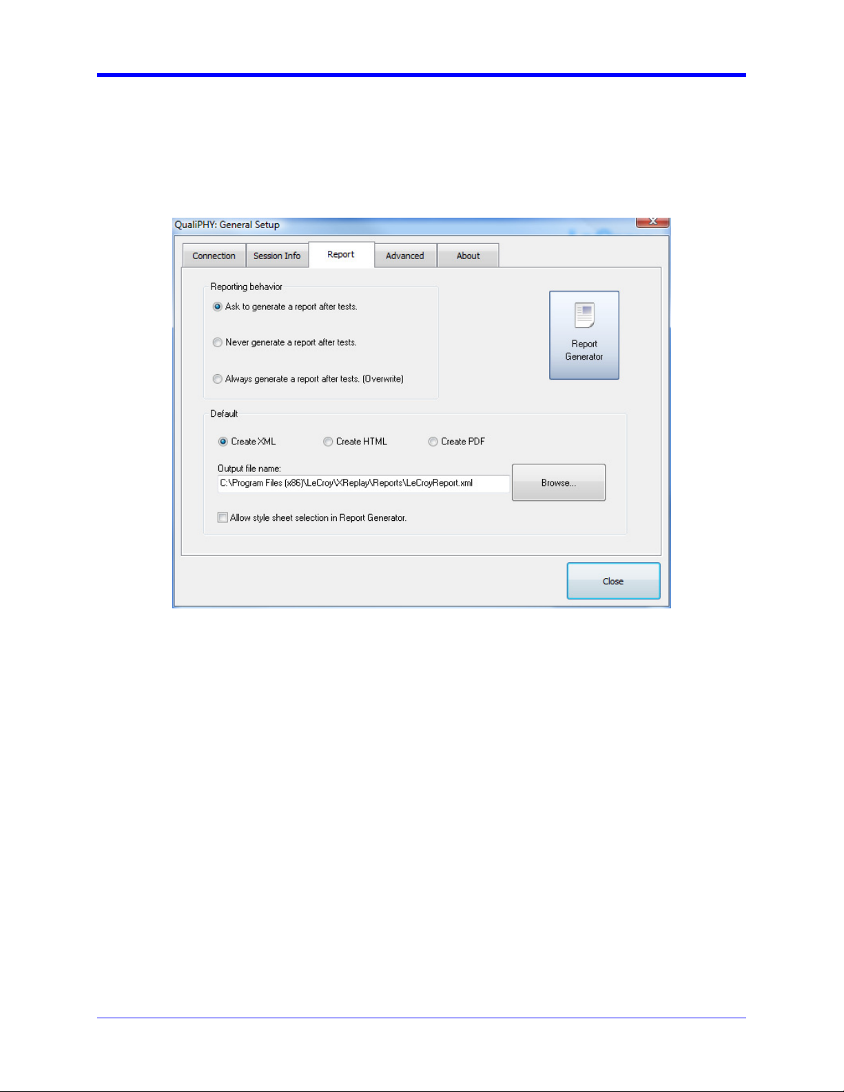
Figure 6. Report menu in QualiPHY General Setup ............................................................................... 11
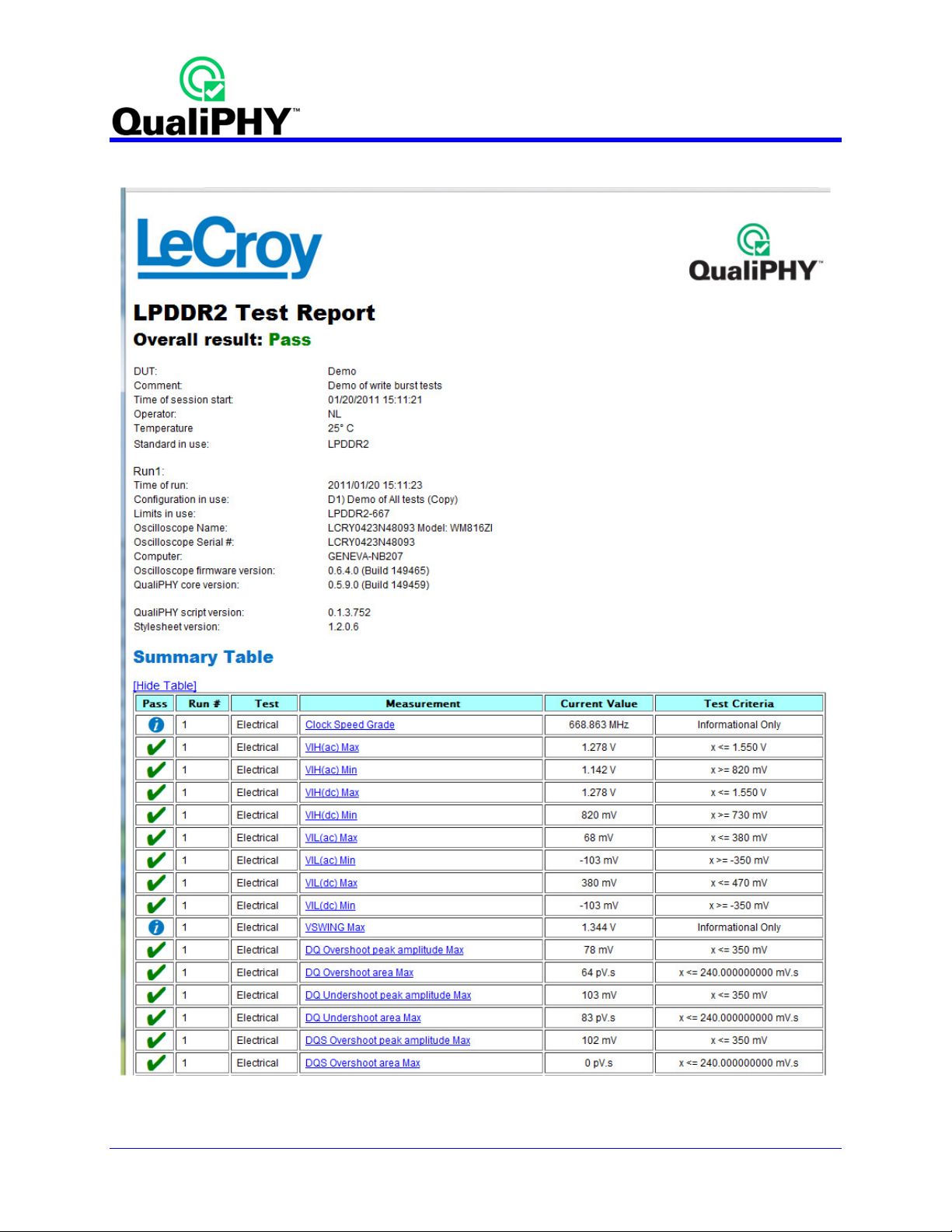
Figure 7. The Test Report includes a summary table with links to the detailed test results ............. 12
Figure 8. QualiPHY main menu and compliance test Standard selection menu ................................ 15
Figure 9. QualiPHY configuration selection menu ................................................................................ 16
Figure 10. QualiPHY test item selection menu ....................................................................................... 18
Figure 11. Variable Setup and Limits Manager windows ...................................................................... 19
Figure 12. Start button .............................................................................................................................. 20
Figure 13. Example of pop-up connection diagram and dialog box .................................................... 20
Figure 14. PCF200 Deskew Fixture ......................................................................................................... 23
Figure 15. Differential probe properly connected to the fixture (Solder-In configuration) ............... 24
Figure 16. Accessing the probe calibration menu ................................................................................. 24
QPHY-LPDDR2-OM-G Rev B
5
Page 6

Figure 17. Basic Probes Calibration menu ............................................................................................. 25
Figure 18. Advanced Mode Probe Calibration menu ............................................................................. 27
Figure 19. Probes Calibration menu Advanced tab ............................................................................... 28
Figure 20. Data output (read) timing [JESD209-2D figure 23] .............................................................. 39
Figure 21. Differential Input Slew Rate Definitions [JESD209-2D figure 111] ..................................... 41
Figure 22. Differential signal levels [JESD209-2D figure 110] .............................................................. 43
Figure 23. Data output (read) timing [JESD208-2B figure 23] .............................................................. 44
Figure 24. Burst read operation [JESD209-2D figure 25] ...................................................................... 44
Figure 25. Data input (write) timing [JESD209-2D figure 40] ................................................................ 46
Figure 26. Slew Rate [JESD209-2D figure 124] ...................................................................................... 48
Figure 27. Command Input Setup and hold timing [JESD209-2D figure 22] ....................................... 49
6
QPHY-LPDDR2-OM-G Rev B
Page 7

QPHY-LPDDR2 Software Option
INTRODUCTION TO QPHY-LPDDR2
QPHY-LPDDR2 is an automated test package performing all of the real time oscilloscope tests for Double
Data Rate in accordance with JEDEC Standard No. 209-2B. The software can be run on the LeCroy
SDA/DDA/WavePro 740Zi and 760Zi, all SDA/DDA/WaveMaster 8Zi, and WaveRunner 625Zi and
WaveRunner 640Zi oscilloscopes.
Required equipment
• SDA/DDA/WavePro 740/760Zi or SDA/DDA/WaveMaster 8Zi or WaveRunner 640Zi/625Zi
oscilloscope
• Four D620 Probes with WL-Plink Prolink probe body
• Alternatively, D610 probes may be used if the voltage swing of the signal is within +/- 2.5Vp-p.
• TF-DSQ Probe Deskew and Calibration Fixture (not needed if using a Zi oscilloscope)
SIGNALS MEASURED
The compliance test requires probing the following signals (# is the negative polarity of the differential
signal):
CK, CK# Input
Clock: CK and CK# are differential clock inputs. All address and control input signals are sampled on the
crossing of the positive edge of CK and negative edge of CK#. Output (read) data is referenced to the
crossings of CK and CK# (both directions of crossing).
DQ Input/Output
Data Input/Output: Bi-directional data bus.
DQS, DQS# Input/Output
Data Strobe: output with read data, input with write data. This signal is in phase with read data and 90
degrees out of phase with write data.
ADD/CTRL
In addition to the Clock, Data and Strobe signals, address and control signals can also be measured.
Bank Address (BA0 – BA2), Chip Select (CS), Command Inputs (RAS, CAS and WE), Clock Enable
(CKE) and On Die Termination (ODT) can all be specified as the signal under test.
BASIC FUNCTIONALITY
The functionality is extracted from JEDEC Standard No. 209-2B.
Read and write accesses to the LPDDR2 SDRAM are burst oriented; accesses start at a selected location
and continue for a burst length of four or eight or sixteen in a programmed sequence. Accesses begin
with the registration of an Active command, which is then followed by a Read or Write command.
Prior to normal operation, the LPDDR2 SDRAM must be initialized.
QPHY-LPDDR2-OM-G Rev B
7
Page 8
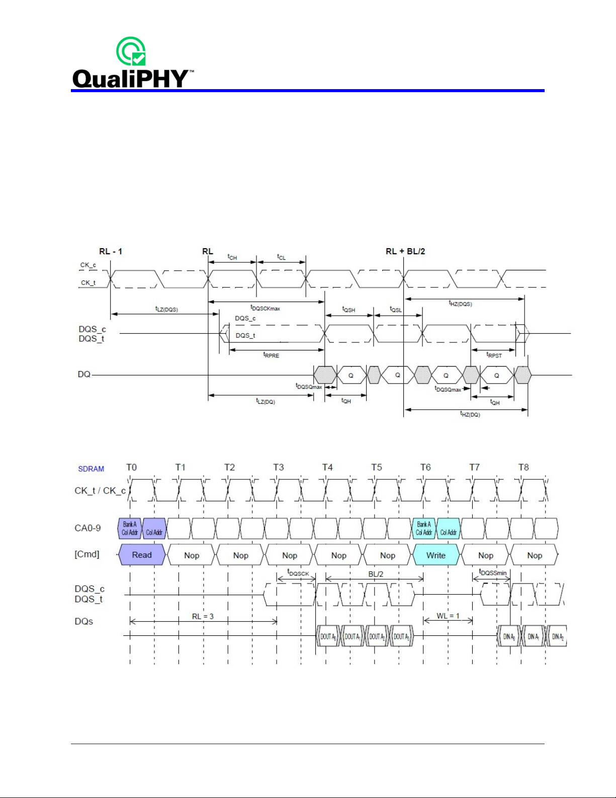
Burst Read
The Burst Read command is initiated by having CS_n LOW, CA0 HIGH, CA1 LOW and CA2 HIGH at the
rising edge of the clock. The command address bus inputs, CA5r-CA6r and CA1f-CA9f, determine the
starting column address for the burst. The Read Latency (RL) is defined from the rising edge of the clock
on which the Read Command is issued to the rising edge of the clock from which the tDQSCK delay is
measured. The first valid datum is available RL * tCK + tDQSCK + tDQSQ after the rising edge of the
clock where the Read Command is issued. The data strobe output is driven LOW tRPRE before the first
rising valid strobe edge. The first bit of the burst is synchronized with the first rising edge of the data
strobe. Each subsequent data-out appears on each DQ pin edge aligned with the data strobe. The RL is
programmed in the mode registers.
Figure 1. Data output (read) timing [JESD209-2D figure 23]
Figure 2. Burst read followed by burst write [JESD209-2D figure 32]
The minimum time from the burst read command to the burst write command is defined by the Read
Latency (RL) and the Burst Length (BL). Minimum read to write latency is RL + RU(tDQSCKmax/tCK) +
8
QPHY-LPDDR2-OM-G Rev B
Page 9
QPHY-LPDDR2 Software Option
BL/2 + 1 - WL clock cycles. Note that if a read burst is truncated with a Burst Terminate (BST) command,
the effective burst length of the truncated read burst should be used as “BL” to calculate the minimum
read to write delay.
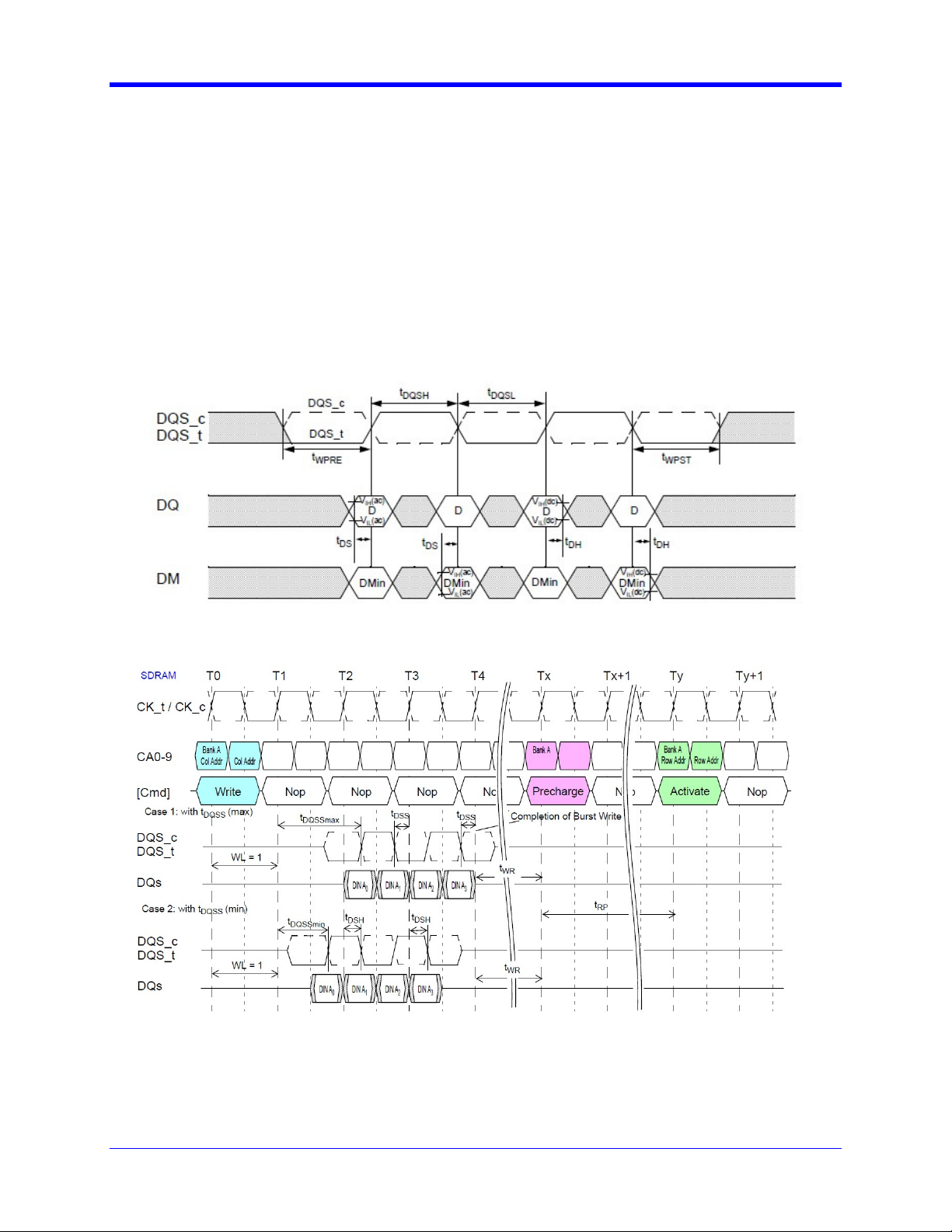
Burst Write
The Burst Write command is initiated by having CS_n LOW, CA0 HIGH, CA1 LOW and CA2 LOW at the
rising edge of the clock. The command address bus inputs, CA5r-CA6r and CA1f-CA9f, determine the
starting column address for the burst. The Write Latency (WL) is defined from the rising edge of the clock
on which the Write Command is issued to the rising edge of the clock from which the tDQSS delay is
measured. The first valid datum shall be driven WL * tCK + tDQSS from the rising edge of the clock from
which the Write command is issued. The data strobe signal (DQS) should be driven LOW tWPRE prior to
the data input. The data bits of the burst cycle must be applied to the DQ pins tDS prior to the respective
edge of the DQS and held valid until tDH after that edge. The burst data are sampled on successive
edges of the DQS until the burst length is completed, which is 4, 8, or 16 bit burst.
Figure 3. Data input (write) timing [JESD209-2D figure 40]
Figure 4. Burst write: WL = 1, BL = 4 [JESD209-2D figure 41]
QPHY-LPDDR2-OM-G Rev B
9
Page 10
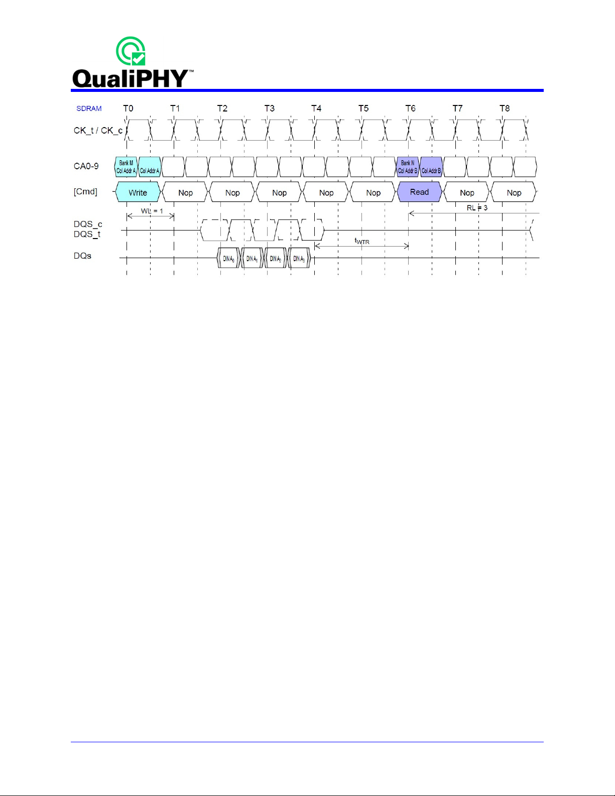
Figure 5. Burst write followed by burst read [JESD209-2D-2E figure 44]
USING QUALIPHY LPDDR2
QualiPHY LPDDR2 guides the user, step-by-step, through each of the source tests described in JEDEC
Standard No. 209-2B. To do this, the user must setup a test session.
Users choose test configurations to run. There are several pre-loaded test configurations including:
• 1) Clock tests LPDDR2-667 (1 Probe)
• 2) CKdiff-DQse-DQSdiff 667 Write Burst (3 probes)
• 3) CKdiff-DQse-DQSdiff 667 Read Burst (3 probes)
• 4) Eye Diagram (3 Probes Debug)
• 5) Addr/Cmd tests (4 Probes)
• D3) Demo of All tests
The pre-loaded configurations provide quick and easy ways to begin compliance testing. You can create
your own custom configurations (see the Customizing QualiPHY topic for details).
The variables are pre-loaded with the standard settings for compliance testing; however, the user may
choose to create their own configuration with the variables set as desired.
10
QPHY-LPDDR2-OM-G Rev B
Page 11
QPHY-LPDDR2 Software Option
QUALIPHY COMPLIANCE TEST PLATFORM
QualiPHY is LeCroy’s compliance test framework which leads the user through the compliance tests.
QualiPHY displays connection diagrams to ensure tests run properly, automates the oscilloscope setup,
and generates complete, detailed reports.
The QualiPHY software application automates the test and report generation.
Figure 6. Report menu in QualiPHY General Setup
QPHY-LPDDR2-OM-G Rev B
11
Page 12
See the QualiPHY Operator’s Manual for more information on how to use the QualiPHY framework.
Figure 7. The Test Report includes a summary table with links to the detailed test results
12
QPHY-LPDDR2-OM-G Rev B
Page 13

QPHY-LPDDR2 Software Option
Oscilloscope Option Key Installation
An option key must be purchased to enable the QPHY-LPDDR2 option. Call LeCroy Customer Support to
place an order and receive the code.
Enter the key and enable the purchased option as follows:
1. From the oscilloscope menu select Utilities Utilities Setup
2. Select the Options tab and click the Add Key button.
3. Enter the Key Code using the on-screen keyboard.
4. Restart the oscilloscope to activate the option after installation.
Typical (Recommended) Configuration
QualiPHY software can be executed from the oscilloscope or a host computer. The first step is to install
QualiPHY. Please refer to the QualiPHY Operator’s Manual for installation instructions.
LeCroy recommends running QualiPHY on an oscilloscope equipped with Dual Monitor Display capability
(Option DMD-1 for oscilloscopes where this is not standard). This allows the waveform and
measurements to be shown on the oscilloscope LCD display while the QualiPHY application and test
results are displayed on a second monitor.
By default, the oscilloscope appears as a local host when QualiPHY is executed in the oscilloscope.
Follow the steps under Oscilloscope Selection (as follows) and check that the IP address is 127.0.0.1.
Remote (Network) Configuration
It is also possible to install and run QualiPHY on a host computer, controlling the oscilloscope with a
Network/LAN Connection.
The oscilloscope must already be configured, and an IP address (fixed or network-assigned) must already
be established.
Oscilloscope Selection
Set up the oscilloscope using QualiPHY over a LAN (Local Area Network) by doing the following:
1. Make sure the host computer is connected to the same LAN as the oscilloscope. If unsure, contact
your system administrator.
2. From the oscilloscope menu, select Utilities Utilities Setup
3. Select the Remote tab.
4. Verify the oscilloscope has an IP address and the control is set to TCP/IP.
5. Run QualiPHY in the host computer and click the General Setup button.
6. Select the Connection tab.
7. Enter the IP address from step 4 (previous).
8. Click the Close button.
QualiPHY is now ready to control the oscilloscope.
QPHY-LPDDR2-OM-G Rev B
13
Page 14

QualiPHY tests the oscilloscope connection after clicking the Start button. The system prompts you if
there is a connection problem. QualiPHY’s Scope Selector function can also be used to verify the
connection. Please refer to the QualiPHY Operator’s Manual for explanations on how to use Scope
Selector and other QualiPHY functions.
Accessing the QPHY-LPDDR2 Software using QualiPHY
This topic provides a basic overview of QualiPHY’s capabilities. Please refer to the QualiPHY Operator’s
Manual for detailed information.
Access the QPHY-LPDDR2 software using the following steps:
1. Wait for the oscilloscope to start and have its main application running.
2. Launch QualiPHY from the Analysis menu if installed on the oscilloscope or from the desktop icon if
installed on a host computer.
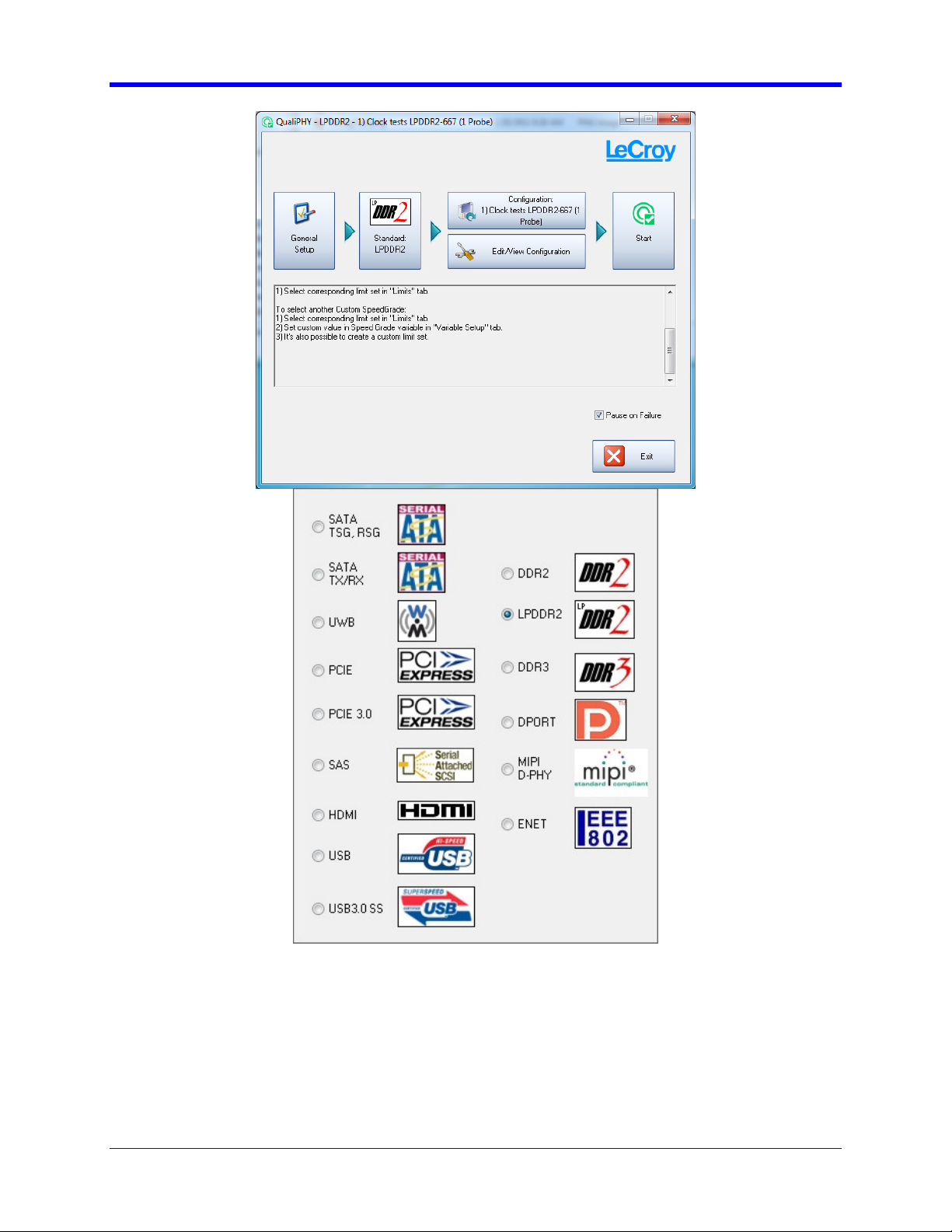
3. From the QualiPHY main window (as follows), select Standard, then LPDDR2 from the pop-up menu
(if not already selected). If you check the Pause on Failure box (circled) QualiPHY prompts to retry
the test in the case of a failure.
14
QPHY-LPDDR2-OM-G Rev B
Page 15
QPHY-LPDDR2 Software Option
Figure 8. QualiPHY main menu and compliance test Standard selection menu
QPHY-LPDDR2-OM-G Rev B
15
Page 16

4. Click the Configuration button in the QualiPHY main menu:
5. Select a configuration from the pop-up menu:
Figure 9. QualiPHY configuration selection menu
6. Click Start.
7. Follow the pop-up window prompts.
16
QPHY-LPDDR2-OM-G Rev B
Page 17

QPHY-LPDDR2 Software Option
Customizing QualiPHY
The predefined configurations in the Configuration screen cannot be modified. However, you can create
your own test configurations by copying one of the standard test configurations and making modifications.
A description of the test is also shown in the description field when selected.
QPHY-LPDDR2-OM-G Rev B
17
Page 18

Figure 10. QualiPHY test item selection menu
18
QPHY-LPDDR2-OM-G Rev B
Page 19

QPHY-LPDDR2 Software Option
Once a custom configuration is defined, script variables and the test limits can be changed by using the
Variable Setup and Limits Manager from the Edit/View Configuration window.
Figure 11. Variable Setup and Limits Manager windows
QPHY-LPDDR2-OM-G Rev B
19
Page 20

QPHY-LPDDR2 Operation
After pressing Start in the QualiPHY menu, the software instructs how to set up the test using pop-up
connection diagrams and dialog boxes.
Figure 12. Start button
Figure 13. Example of pop-up connection diagram and dialog box
20
QPHY-LPDDR2-OM-G Rev B
Page 21

QPHY-LPDDR2 Software Option
LPDDR2 MEASUREMENT PREPARATION
Before starting any test or data acquisition, the oscilloscope must be warmed for at least 20 minutes.
Calibration is automatic under software control and no manual calibration is required. The procedure
should be run again if the temperature of the oscilloscope changes by more than a few degrees.
Differential Probe Deskew Procedure using TF-DSQ
Note: Another procedure can be used for Zi oscilloscopes, refer to the next section for details.
Follow the procedure described in the TF-DSQ Probe Deskew and Calibration Fixture manual. Deskew all
four channels with their respective probe, using external trigger (AUX IN) as reference signal.
You can get more information on TF-DSQ using the oscilloscope Help menu and searching for Probe
Calibration. There is also a section on Deskew Theory of Operation.
Differential Probe Deskew Procedure on Zi oscilloscopes using PCF200
Use the PCF200 Characterization Fixture provided as standard accessory with WaveLink series probes.
The fixture determines the effect of probe input loading on the circuit under test and the probe response
to the signal being measured, using the AT, ST, Dx10, and Dx20 modules with SI, or SP, or QC (QC for
WL-Plink only) interconnect leads.
Probe calibration is accomplished with the PCF200 fixture by following the basic steps in the following
flowchart. It is recommended that you read the instructions presented here in their entirety to familiarize
yourself with the advanced features of the PCF200 fixture.
Connecting probes to the circuit under test can be a difficult procedure. With this in mind, LeCroy's system
is designed in a manner that allows you to set up the probe calibration fixture, calibrate each individual
probe once, connect your probes to the circuit, and disconnects the fixture. Once your probes are in the
circuit, there is no need to revisit the fixture until the next calibration interval.
You should familiarize yourself with the following topics:
•
QPHY-LPDDR2-OM-G Rev B
21
Page 22

signed in a manner that allows you to set up
the probe calibration fixture, calibrate each individual probe once, connect your
PCF200 Fixture Overview
• Probe Connection to PCF200
• Probe Calibration Menu
• D620 Probe Calibration
Advanced mode is available:
• Advanced Mode Probe Calibration Menu
• Advanced Probe Calibration
Read
about
PCF200
fixture
Connect
PCF200
fixture to
oscillocope
Access
Probe
Calibration
Menu
Connect
Probe to
Fixture
Perform
Probe
Calibration
Disconnect
Probe from
Fixture
Connect Probe
to Circuit and
Make
Measurements
Repeat
this
procedure
for each
probe
Connecting probes to the circuit under test can be a difficult procedure. With
this in mind, LeCroy's system is de
probes to the circuit, and disconnect the fixture. Once your probes are in the
circuit, there is no need to revisit the fixture until the next calibration interval.
You should familiarize yourself with the following topics:
• PCF200 Fixture Overview
• Probe Connection to PCF200
• Probe Calibration Menu
• D620 Probe Calibration
Advanced mode is available:
• Advanced Mode Probe Calibration Menu
• Advanced Probe Calibration
22
QPHY-LPDDR2-OM-G Rev B
Page 23

QPHY-LPDDR2 Software Option
PCF200 Fixture Overview
Major components of the PCF200 fixture are shown in the following figure:
• SMA male connector Fast Edge input.
• SMA female connector output to AUX IN for 50-ohm termination.
• Clip for connection of Solder-In probes.
• 2-pins header for connection of Square-Pin probes.
Figure 14. PCF200 Deskew Fixture
A SMA male to BNC male 50-ohm cable is required to perform the calibration.
System assembly is accomplished in the following steps:
1.
Connect the BNC end of the 50 Ohm cable to the oscilloscope AUX IN.
2.
Connect the SMA end of the 50 Ohm cable to the SMA female connector on the PCF200 fixture.
3.
Connect the PCF200 SMA male connector to the oscilloscope Fast Edge SMA output.
The SMA connections should be torqued with an RF torque wrench and must be properly tightened.
Probe Connection to PCF200
The PCF200 provides multiple probe connectors for various kinds of probes. There are 2 circuits
depending on the type of probes to calibrate:
• The upper circuit is for Solder-In (SI) and Quick-Connect (QC) probes. This circuit can also be
used for AT probes using the designated area to apply the probe tips.
• The lower circuit is for Square-Pin (SP) probes.
QPHY-LPDDR2-OM-G Rev B
23
Page 24

Probes are connected electrically in a single-ended arrangement: the positive (+) side of the probe must
be connected to the signal trace, while the negative (-) side is connected to the ground plane.
Figure 15. Differential probe properly connected to the fixture (Solder-In configuration)
Probe Calibration Menu
The probe calibration menu can be accessed from the Vertical drop-down menu or from the channel
dialog:
Figure 16. Accessing the probe calibration menu
24
QPHY-LPDDR2-OM-G Rev B
Page 25

QPHY-LPDDR2 Software Option
Figure 17. Basic Probes Calibration menu
The information in the probe calibration menu is organized such that each row represents the information
for a given channel, and each column represents the calibration information or control for that channel.
For each channel, the information and control provided includes:
• The channel number in the colored button icon and the probe type that is installed.
• A Full Calibration button, which starts the calibration. Use only with TF-DSQ. DO NOT use with
PCF200.
• DC correction information including both gain and offset correction.
• The skew correction.
• A Clear button.
Probe
This area shows the type of probe connected to the channel. All other information shown in a given row is
associated with that probe.
Full Calibration Button
This button causes the oscilloscope to automatically perform a full DC and deskew calibration. See details
of DC Calibration Theory of Operation and Deskew Theory of Operation in TF-DSQ Operation Manual.
Use only with TF-DSQ. DO NOT use with PCF200.
Gain & Offset
These fields show the gain and offset applied to the probe. If the probe measures a voltage of V, the new,
calibrated voltage is:
OffsetGainVV
calibrated
Note that the offset is in Volts, and the gain is unitless.
The probe DC calibration information can be entered either manually or as the result of an automatic
calibration. In the case of automatic calibration, it can be part of the full calibration or it can be a
standalone DC calibration executed in advanced mode. When the DC calibration information is a result of
an automatic calibration utilizing the TF-DSQ fixture, the information shown is the gain and offset utilized
for the currently configured channel sensitivity (volt/division setting; see details of DC Calibration Theory
of Operation in the TF-DSQ Operator’s Manual on the LeCroy website for details). In this case, when the
channel sensitivity is altered these values change. When the DC calibration information is entered
manually, it clears any automatic results and replaces them globally with the newly entered
values. This means that if new gain and offset numbers are entered manually, these values apply
across all sensitivity oscilloscope settings.
+⋅=
The gain is limited to between 0.8 and 1.2, but the offset is not limited.
QPHY-LPDDR2-OM-G Rev B
25
Page 26

Note: It is important to note that some passive probes, and any user-designed probes, do not provide proper probe identification
information to the oscilloscope. In these cases, the oscilloscope may not be able to determine the proper attenuation values and you
should make sure that the proper attenuation is entered from the channel’s Vertical setup dialog. Furthermore, the gain entered
should be the gain correction applied to the system with the correctly entered attenuation.
If used with PCF200, enter values manually.
Skew
This field shows the measured skew between the probe in the specified channel and the reference
channel. This can be entered manually or as the result of an automatic calibration. In the case of
automatic calibration, it can be the result of a portion of the full calibration or it can be the result of a
standalone deskew calibration. Even after the deskew has been performed automatically, the deskew
correction can be adjusted manually.
Clear
All probe calibrations can be cleared by pressing this button corresponding to a specific probe.
Calibration Source
This field specifies the signal source used for DC calibrations. When using the PCF200 fixture, specify
AUX OUT as the calibration source (even if the PCF200 is connected to Fast Edge output). This signal is
not used for deskew.
Calibration Skew Reference
These values specify the channel or external input where the skew reference is supplied. The skew
reference is the absolute time reference to which all deskew measurements are made. When the PCF200
fixture is used, select the EXT input.
Recall Calibration
Whenever a probe calibration is applied, the oscilloscope saves the information in a file on the disk. If the
oscilloscope must be rebooted for any reason, the probe calibration information is always cleared, but can
be manually recalled by pressing this button.
Advanced Mode Checkbox
When the Advanced Mode checkbox is unchecked, you have access to the basic probe calibration
menu. The basic probe calibration menu shows you only what is absolutely needed to perform a simple
calibration of the probes. In other words, it shows you the calibration information and provides the
capability to calibrate the probe with a single button press, clear the calibration information, and manually
reload the calibration information following an oscilloscope reboot. When the advanced mode button is
checked, you have access to the advanced mode probe calibration menu.
This checkbox must be checked for deskew calibration using PCF200.
Advanced Mode Probe Calibration Menu
The advanced mode is entered by checking the advanced mode box in the basic probe calibration menu.
26
QPHY-LPDDR2-OM-G Rev B
Page 27

QPHY-LPDDR2 Software Option
Figure 18. Advanced Mode Probe Calibration menu
QPHY-LPDDR2-OM-G Rev B
27
Page 28

Checking this box allows:
Calibration of gain/offset only
Calibration of deskew only
Access to the advanced menu (shown as a tab behind the "Probes Cal" dialog)
Gain/Offset Only
Pressing this button performs only the DC calibration of the probe on the specified channel. See details of
DC Calibration Theory of Operation in TF-DSQ Operation Manual. DO NOT use with PCF200 connected
to Fast Edge output.
Deskew Only
Pressing this button performs only the deskew calibration of the probe on the specified channel. See
details of Deskew Theory of Operation in TF-DSQ Operation Manual.
This is the button to use with PCF200 connected to Fast Edge output.
The Advanced Menu
Figure 19. Probes Calibration menu Advanced tab
The Advanced Menu contains information and functionality useful to the advanced user of the PCF200
fixture. These include:
• Rise Time Skew Correction
• Differential(or Single-Ended) probe selection
• Deskew All (or common deskew capability)
• Common mode voltage settings for DC calibration
Rise Time Skew Correction
This field shows the signal risetime and the corresponding skew correction based on the signal risetime.
When probes are deskewed, the risetime measurement of the edge used for deskewing is displayed in
the Rise Time field corresponding to the probe and probe channel, and an additional skew correction of
zero is applied.
The measured risetime of the signals encountered can be entered into the Rise Time field, and the
oscilloscope automatically calculates and applies a new skew correction value to be utilized in addition to
the deskew amount calculated during the deskew calibration procedure. With this use, a finer deskew
calibration is performed because the risetimes of the signals measured are now taken into account. Refer
to the Deskew Risetime Adjustment Theory of Operation in the TF-DSQ Operator’s Manual on the LeCroy
website for details.
28
QPHY-LPDDR2-OM-G Rev B
Page 29

QPHY-LPDDR2 Software Option
Differential (or Single-Ended) Probe Selection
The PCF200 fixture calibrates probes differentially or in single-ended mode depending on the type of
probe used. The selection is done automatically when the probe is detected. If No Probe is detected, the
selection is done manually. When calibrating D620 probes, they are automatically detected and
Differential is checked.
Deskew All (or Common Skew)
This is the deskew amount applied to all channels. The time entered in this field is the absolute time by
which all waveforms displayed by the oscilloscope are delayed in time. This value effectively adjusts the
zero time reference of the system. See Deskew Theory of Operation in the TF-DSQ Operation Manual for
details.
Common Mode Voltage Selection
Differential probes allow the common mode voltage component to be applied during the DC calibration for
improved calibration accuracy in situations where probe gain or offset correction depends on common
mode components. See DC Calibration Theory of Operation or Differential and Single-ended Probe
Basics in TF-DSQ Operation Manual for details.
Advanced Probe Calibration
When the Advanced Mode checkbox is checked, you can perform the DC calibration and the deskew
calibration separately by pressing Gain/Offset Only or Deskew Only.
When performing DC calibration, you have the option to apply a common mode component to the
differential DC levels applied to the probe during calibration. See DC Calibration Theory of Operation or
Differential and Single-ended Probe Basics in TF-DSQ Operation Manual for details. Use this with TFDSQ. DO NOT use with PCF200 connected to Fast Edge output.
After performing the deskew calibration, you have the option to apply a common skew value to all
channels to adjust the zero time reference of the system.
If you know the risetime of the signals being measured, you can enter the measured risetime of the
signals in the Rise Time field to obtain a further skew correction that accounts for the risetime. If the
risetime entered is less than the risetime measured during the calibration, no correction is applied;
otherwise, the system calculates a correction to account for the signal risetime. This makes it important to
enter the measured risetime, meaning, the risetime of the signal the oscilloscope measures (or will
measure). Refer to the Deskew Risetime Adjustment Theory of Operation in the TF-DSQ Operator’s
Manual on the LeCroy website for details.
D620 Probe Calibration Procedure
The PCF200 fixture is used to calibrate D620 probes. Prior to beginning your measurements
Assemble the PCF200 fixture
Attach the fixture, as described in PCF200 Fixture Overview.
Access the Probe Calibration Menu in Advanced Mode
Follow the instructions for each probe used:
Connect the probe to the oscilloscope channel
Attach the probe to the PCF200 fixture
Press the Deskew Only button in the Advanced Probe Calibration Menu.
Wait a few seconds as the probe is calibrated.
When the calibration completes, remove the probe from the PCF200 fixture
QPHY-LPDDR2-OM-G Rev B
29
Page 30

Now you are ready to probe the circuit and perform your measurements. If power is interrupted during
your measurements, reboot the oscilloscope and manually recall your settings.
30
QPHY-LPDDR2-OM-G Rev B
Page 31

QPHY-LPDDR2 Software Option
QPHY-LPDDR2 TEST CONFIGURATIONS
Configurations include variable settings and limit sets as well, not just test selections. See the section for
a description of each variable value and its default value. See the QPHY-LPDDR2 Limit Sets section for
more information about the limit sets.
1) Clock tests LPDDR2-667 (1 Probe)
This configuration runs all of the clock tests. All of the variables are set to their defaults. The limit set in
use is LPDDR2-667. The tests run are:
• tCK(avg)
• tCK(abs)
• tCK(min)
• tCH(avg)
• tCH(abs)
• tCL(avg)
• tCL(abs)
• tJIT(per)
• tJIT(CC)
• tERR(n per)
2) CKdiff-DQse-DQSdiff 667 (3 probes)
This configuration runs all of the tests that are run on write bursts of the LPDDR2 signals in which 3
probes are required. All of the variables are set to their defaults. The limit set in use is LPDDR2-667. The
tests run are:
• Eye Diagram – Write Bursts (Inputs)
• Eye Diagram – Read Bursts
• tDQSQ
• tQH
• tDS (base + derated)
• tDH (base + derated)
• tDQSH
• tDQSL
• tDQSS – min
• tDQSS – max
• tDSS
• tDSH
• tWPST
• tWPRE
• tRPRE
QPHY-LPDDR2-OM-G Rev B
31
Page 32

• tRPST
• tDIPW
• tQSH
• tQSL
• tQHP
• tQHS for DQx
• tDQSCK
• tVAC for DQx
• tDS/tDH (vref based)
• tHZ(DQ)
• tHZ(DQS)
• tLZ(DQS)
• tLZ(DQ)
• VIHDQ(AC)
• VIHDQ(DC)
• VILDQ(AC)
• VILDQ(DC)
• VOH(ac)
• VOL(ac)
• SRQ diff-rise(DQS)
• SRQ diff – fall(DQS)
• SRQse – Rise
• SRQse –Fall
• Overshoot Amplitude
• Undershoot Amplitude
• Overshoot Area
• Undershoot Area
• Data Eye Height
3) 4 Probe tests
• VIH/VIL on CLK+/- and DQS +/-
• Overshoot and undershoot for CLK +/-
• tDVAC at rising and falling edge for CLK+/-, DQSx+/- and DQx
• VSEH/VSEL(ac) for DQSx+/-
32
QPHY-LPDDR2-OM-G Rev B
Page 33

QPHY-LPDDR2 Software Option
• Write slew rate of rising and falling edge for CLK+/-, DQSx+/- and DQx
• VIX for CLK +/- and DQSx+/-
• Vref(dc)
• Slew rate of rising and falling edge for Cax or other control signals
• VIH(ac) and VIL(ac) for CAx or other control signals
• AC overshoot and undershoot for CAx or other control signals
• tIS (base) on rising and falling edge for CAx ot other control signals
• tIH (base) on rising and falling edge for CAx or other control signals
• tIPW
QPHY-LPDDR2-OM-G Rev B
33
Page 34

D2) Demo of Eye Diagram (Debug)
This configuration uses the saved waveforms found in the D:\Waveforms\LPDDR2 folder and run the
Eye Diagram test on the read bursts and the write bursts. All of the variables are set to their defaults
except Use Stored Waveforms is set to Yes and Use Stored Trace for Speed Grade is set to Yes. The
limit set in use is LPDDR2-667. The tests run are:
• Eye Diagram – Write Bursts (Inputs)
• Eye Diagram – Read Bursts (Outputs)
D3) Demo of All tests
This configuration uses the saved waveforms found in the D:\Waveforms\LPDDR2 folder and run all of
the tests. All of the variables are set to their defaults except Use Stored Waveforms is set to Yes and
Use Stored Trace for Speed Grade is set to Yes. The limit set in use is LPDDR2-667. All supported tests
are run.
D4) Demo of All CKdiff-DQSdiff-DQse tests
This configuration uses the saved waveforms found in the D:\Waveforms\LPDDR2 folder and run all of
the tests requiring probing the clock and strobe signals differentially and the single ended data signal. All
of the variables are set to their defaults except Use Stored Waveforms is set to Yes and Use Stored
Trace for Speed Grade is set to Yes. The limit set in use is LPDDR2-667. All supported tests are run.
34
QPHY-LPDDR2-OM-G Rev B
Page 35

QPHY-LPDDR2 Software Option
QPHY-LPDDR2 VARIABLES
General Variables
The following variables are used by all configurations. They can be used in conjunction with the test
selection and limit set selection to create custom configurations.
DUT Speed Grade in MT/s
Transfer speed of the DUT. Used to set the oscilloscope timebase and sampling rate, see Clock Period
Per Screen Division variable for more explanation. Choose between: 466, 533, 667, 800, 933 and 1066
MT/s. Default is 667 MT/s.
DQ Signal Name
Select name of data (DQ) SUT. Choose between available DDR signal names. Default is DQ0.
DQS Signal Name
Select name of strobe (DQS) SUT. Choose between available DDR signal names. Default is DQS0.
Clock Signal Name
Select name of clock (CK) SUT. Choose between available DDR signal names. Default is CK.
DUT Power Supply VDDQ
Value of VDDQ used to compute test limits as specified by Jedec standard. Default is 1.8 V.
Script Settings
Save Acquired Waveforms
Saved waveforms can be used later in demonstration or optimized version of script. Choose between Yes
or No. The default is No. This setting is ignored (no save) if using stored waveforms is enabled and in
Demo mode.
Silent mode control
No more interaction with the user when silent mode is on. Choose between Yes or No. Default is No. This
is useful to let the test run without interruption in the background.
Stop On Test to review results
When set to Yes, the script stops after each test allowing you to view the results. The setup is saved so
the oscilloscope settings can be modified by the user. On resume, the setup is recalled. Any new
acquisition done may cause the script to produce unexpected results.
Waveform Path
Specify the path on the oscilloscope to save/recall waveforms. When not in Demo Mode and when Save
acquired waveforms is enabled, the waveforms are saved in this folder. When set to Demo Mode or
when Use stored trace for pixel clock measure, waveforms are also available from this folder. The
default location is D:\Waveforms\LPDDR2.
Demo Settings
Use Stored Waveforms
When enabled, previously stored LPDDR2 waveforms is used. Default is No.
Recalled Waveform File Index (5 digits)
Enter the 5 digits number corresponding to the index of the file you want to recall. Default is 00000.
QPHY-LPDDR2-OM-G Rev B
35
Page 36

Define format used to set trace names
Stores a saved waveform naming format or convention The choices are LeCroy or Dialog. The LeCroy
choice produces waveform names automatically by the software. Dialog prompts the user for custom
waveform names. The default setting is LeCroy.
Use Stored Trace for Speed Grade
This is an optimization used specifically to measure the clock frequency only once. Choose from Yes or
No values, The default selection is No.
Advanced Settings
Clock Period per Screen Division
Oscilloscope timebase and sampling rate is set to acquire the given number of clock cycle per display
horizontal division at a given DUT Speed Grad in MT/s and for a Max. Number of Samples Per Clock
Period. The default is 3341 clock periods (this gives a 10us/div timebase at 667 MT/s and 3.3MS max for
100 samples per period).
Timebase = [Clock Period Per Screen Division] / ([DUT Speed Grade in MT/s] / 2 * 1e6)
Maximum Samples = [Max. Number Of Samples Per Clock Period] * [Clock Period Per Screen
Division] * 10
Number of cycles for Clock test
Jedec standard requires 200 cycles for the Clock compliance test.
This is the default value of this variable. Any positive number can be entered.
Max. Number Of Samples Per Clock Period
The oscilloscope timebase and sampling rate is set to acquire the given number of points per clock
period. The oscilloscope is always set to at least acquire at 20GS/s. Additionally, if an oscilloscope with
greater than 6GHz bandwidth is used, the bandwidth is limited to 6GHz. See the Clock Period Per
Screen Division topic for more details. Choose between 10;20;50;100;200;500 or 1000. The default
value is 100.
Configuration Specific Variables
The following variables are specific to the configuration in which they appear under. Some of these
variables appear under multiple configurations.
XX Channel Gain
Allows the user to manually specify the vertical scale in V/div for XX SUT. XX can be Clock, DQ, DQS,
DQSn, ADD/CTRL, or DM. Default is 0 for auto-scale.
XX Channel Index
Allows the user to manually specify the channel XX SUT. XX can be Clock, DQ, DQS, DQSn, ADD/CTRL,
or DM. Default is 1 for CK, 2 for DQS, 3 for DQ and 4 for others
XX Channel Invert
Allows the user to invert XX SUT. XX can be Clock, DQ, DQS, DQSn, ADD/CTRL, or DM. Default is
False.
XX Channel Offset
Allows the user to manually specify the offset in Volts for XX SUT. XX can be Clock, DQ, DQS, DQSn,
ADD/CTRL, or DM. Default is 0 for auto-scale.
36
QPHY-LPDDR2-OM-G Rev B
Page 37

QPHY-LPDDR2 Software Option
Select Signal Under Test if many
These variables allow the user to specify which signals to tests for particular tests. The default state is to
tests all of the pertinent signals. For the ADD/CTRL tests the default is ADD and for the DM tests the
default is DM
Note: Register vendor data sheets specify the maximum over/undershoot induced in specific RDIMM applications. DRAM vendor
data sheets also specify the maximum overshoot/undershoot that their DRAM can tolerate. This allows the RDIMM supplier to
understand whether the DRAM can tolerate the overshoot that the register induces in the specific RDIMM.
QPHY-LPDDR2-OM-G Rev B
37
Page 38

QPHY-LPDDR2 LIMIT SETS
LPDDR2-466
This corresponds to the JEDEC JESD209-2D LPDDR2 standard specification limits for 466 MT/s.
LPDDR2-533
This corresponds to the JEDEC JESD209-2D LPDDR2 standard specification limits for 533 MT/s.
LPDDR2-667
This corresponds to the JEDEC JESD209-2D LPDDR2 standard specification limits for 667 MT/s.
LPDDR2-800
This corresponds to the JEDEC JESD209-2D LPDDR2 standard specification limits for 800 MT/s.
LPDDR2-933
This corresponds to the JEDEC JESD209-2D LPDDR2 standard specification limits for 933 MT/s.
LPDDR2-1066
This corresponds to the JEDEC JESD209-2D LPDDR2 standard specification limits for 1066 MT/s.
QPHY-LPDDR2 TESTS
Clock Tests
All time measure on clock CK are done at level VREF.
tCK(avg), Average Clock Period
tCK(avg) is defined as the average clock period over any 200 consecutive clock periods.
tCK(avg) = SUM(tCKi) / 200 where i=1 to 200
Measured on both the rising and the falling edge.
tCK(abs), Absolute Clock Period
tCK(abs) is defined as the absolute clock period of each of 200 consecutive clock periods.
Measured on both the rising and the falling edge.
38
QPHY-LPDDR2-OM-G Rev B
Page 39

QPHY-LPDDR2 Software Option
tCH(avg), Average High Pulse Width
tCH(avg) is defined as the average high pulse width, as calculated across any consecutive 200 high
pulses.
tCH(avg) = SUM(tCHi) / (200 x tCK(avg)) where I = 1 to 200
See Figure 20 as follows.
tCL(avg), Average Low Pulse Width
tCL(avg) is defined as the average low pulse width, as calculated across any consecutive 200 low pulses.
tCL(avg) = SUM(tCLi) / (200 x tCK(avg)) where i=1 to 200
See Figure 20 as follows.
Figure 20. Data output (read) timing [JESD209-2D figure 23]
tCH(abs), Absolute High Pulse Width
tCH(abs) is defined as the absolute high pulse width, of each of 200 consecutive high pulses.
tCL(abs), Absolute Low Pulse Width
tCL(abs) is defined as the absolute low pulse width of each of 200 consecutive low pulses.
QPHY-LPDDR2-OM-G Rev B
39
Page 40

tJIT(duty), Half Period Jitter
tJIT(per), Clock Period Jitter
tJIT(per) is defined as the largest deviation of any single tCK from tCK(avg). This test compares the
average clock period (over 200 cycles) with each period inside the window. The smallest and largest
values must be within limits.
tJIT(per) = Min/max of {tCKi - tCK(avg)} where i=1 to 200
Measured on both the rising and the falling edge.
There are different limit depending on whether the DLL is already locked or not:
• tJIT(per) defines the single period jitter when the DLL is already locked.
• tJIT(per,lck) uses the same definition for single period jitter, during the DLL locking period only.
A configuration variable allows to define which limit to use.
tJIT(cc), Cycle to Cycle Period Jitter
tJIT(cc) is defined as the difference in clock period between two consecutive clock cycles. This test
compares the smallest and largest values of the difference between any two consecutive clock cycles
inside a 200 cycles window.
tJIT(cc) = Min/max of {tCKi+1 – tCKi} where i = 1 to 199
Measured on both the rising and the falling edge.
There are different limit depending on whether the DLL is already locked or not:
• tJIT(cc) defines the cycle to cycle jitter when the DLL is already locked.
• tJIT(cc,lck) uses the same definition for cycle to cycle jitter, during the DLL locking period only.
A configuration variable allows to define which limit to use.
tERR(n per), Cumulative Error
tERR is defined as the cumulative error across multiple consecutive cycles from tCK(avg). This test
compares the average clock period (over 200 cycles) with each n-bit period inside the window. The
smallest and largest values must be within limits.
There are 12 different tests:
tERR( n per) (n → 2,3,4,5,6,7,8,9,10,12,13,14…49,50)
tERR(nper) = Min/max of {SUM(tCKi) - n x tCK(avg)}
where i=1 to n and:
40
QPHY-LPDDR2-OM-G Rev B
Page 41

QPHY-LPDDR2 Software Option
n = 2 for tERR(2per)
n = 3 for tERR(3per)
n = 4 for tERR(4per)
n = 5 for tERR(5per)
(and so forth until n = 12)
13 ≤ n ≤ 50 for tERR(11-50per)
Measured on both the rising and the falling edge.
Eye Diagram
Write Burst (Inputs)
This is an informational only test that creates the eye diagram of all of the write bursts found in the
acquisition.
Read Burst (Outputs)
This is an informational only test that creates the eye diagram of all of the read bursts found in the
acquisition.
Electrical Tests
Slew Rate
Please refer to section 8.6 of the JESD209-2D for single ended input signals and to section 8.7 for slew
rate for differential signals.
Figure 21. Differential Input Slew Rate Definitions [JESD209-2D figure 111]
Logic Levels
VIH(ac), maximum AC input logic high
Measure the local maximum value from VREF to VREF of the high pulse histogram. If multiple pulses are
measured, take the lowest number and the highest number as the worst cases.
QPHY-LPDDR2-OM-G Rev B
41
Page 42

The lowest number must be greater than or equal to the minimum limit and the highest number must be
less than or equal to the maximum limit.
VIH(dc), minimum DC input logic high
Measure the local minimum and maximum values from the first VIH(ac)min crossing point to the time
corresponding to VIH(dc)min crossing a 1V/ns slewrate slope to VREF. If multiple pulses are measured,
take the lowest, respectively the highest, number as the worst case.
The local minimum must be greater than or equal to the minimum limit. The local maximum must be less
than or equal to the maximum limit.
VIL(ac), maximum AC input logic low
Measure the local minimum value from VREF to VREF of the low pulse histogram. If multiple pulses are
measured, take the lowest number and the highest number as the worst cases.
The lowest number must be greater than or equal to the minimum limit and the highest number must be
less than or equal to the maximum limit.
VIL(dc), minimum DC input logic low
Measure the local minimum and maximum values from the first VIL(ac)max crossing point to the time
corresponding to VIL(dc)max crossing a 1V/ns slewrate slope to VREF. If multiple pulses are measured,
take the lowest, respectively the highest, number as the worst case.
The local minimum must be greater than or equal to the minimum limit. The local maximum must be less
than or equal to the maximum limit.
VSWING(MAX), input signal maximum peak to peak swing
Measure the peak to peak value of the signal in a given Write frame. .If multiple frames are measured,
take, the highest number as the worst case.
The measure must be less than or equal to the limit.
AC Over/Undershoot
AC Overshoot, Maximum peak amplitude
Maximum peak amplitude allowed for overshoot area.
AC Overshoot, Maximum overshoot area above VDDQ
Prerequisite: AC Overshoot maximum peak amplitude, needed to compute area.
Maximum overshoot area above VDDQ.
42
QPHY-LPDDR2-OM-G Rev B
Page 43

AC Undershoot, Maximum peak amplitude
Maximum peak amplitude allowed for undershoot area.
Figure 22. Differential signal levels [JESD209-2D figure 115]
VIX
QPHY-LPDDR2 Software Option
Figure 23. VIX Definition [JESD209-2D figure 111]
Timing Tests
Read Bursts
tDQSQ, DQS-DQ Skew for DQS and Associated DQ Signals
Maximum skew between the DQS line and the associated DQ line within a read burst
Measure timing from DQS at VREF to DQ rising at VIH(ac)min and falling at VIL(ac)max.
QPHY-LPDDR2-OM-G Rev B
43
Page 44

Figure 24. Data output (read) timing [JESD208-2B figure 23]
tQHS, DQ hold skew factor
This measures DQ at VIH(dc) or VIL(dc) to DQS at VREF
tQH, DQ/DQS Output Hold Time From DQS
This measures the timing from DQS at VREF to DQ at VIH(dc) (rising edge) or VIL(dc) (falling edge).
tQH = tQHP - tQHS
tDQSCK, DQS Output Access Time from CK/CK #
Time from CK at VREF level to DQS at VREF level.
Figure 25. Burst read operation [JESD209-2D figure 25]
This is a measure similar to tDQSS but on the Read.
44
QPHY-LPDDR2-OM-G Rev B
Page 45

QPHY-LPDDR2 Software Option
tHZ(DQ), DQ High Impedance Time From CK/CK#
This is the time from Vref of the CK/CK# signal to the point when the DQ is not being driven anymore (at
the end of the burst)
tLZ(DQ), DQ Low-Impedance Time from CK/CK#
This is the time from when the DQ begins to be driven (at the beginning of the burst) to the nearest
CK/CK# edge.
tLZ(DQS), DQS Low-Impedance Time from CK/CK#
This is the time from when the DQS begins to be driven (at the beginning of the preamble) to the nearest
CK/CK# edge.
tRPRE, Read Preamble
Time from when DQS begins to be driven (at the beginning of the preamble) to when it crosses Vref. This
is only measured on a read cycle.
Prerequisite: tJIT(per), a derating factor is applied to the limit depending on the clock jitter.
tRPST, Read Postamble
Time from when DQS crosses Vref (at the beginning of the postamble) to when DQS stops being driven
(at the end of the postamble). This is only measured on a read cycle.
Prerequisite: tJIT(duty), a derating factor is applied to the limit depending on the clock jitter.
QPHY-LPDDR2-OM-G Rev B
45
Page 46

Write Bursts
tDQSS, DQS latching rising transitions to associated CK edge
CK rising edge at VREF level to DQS rising edge at VREF level, see Figure.
Figure 26. Burst write operation: WL=1 BL=4 [JESD209-2D figure 41]
tDQSH, DQS Input High Pulse Width
DQS High pulse width at VREF level, see Figure 26.
Figure 26. Data input (write) timing [JESD209-2D figure 40]
tDQSL, DQS Input Low Pulse Width
DQS Low pulse width at VREF level, see Figure 26.
46
QPHY-LPDDR2-OM-G Rev B
Page 47

QPHY-LPDDR2 Software Option
tDSS, DQS Falling Edge to CK Setup Time
Time from DQS falling edge at VREF level to CK rising edge at VREF level, see Figure 26.
tDSH, DQS Falling Edge Hold Time from CK
Time from CK rising edge at VREF level to DQS falling edge at VREF level, see Figure 26.
tWPRE, Write Preamble
Time from when DQS begins to be driven (at the beginning of the preamble) to when it crosses Vref. This
is only measured on a write cycle.
tWPST, Write Postamble
Time from when DQS crosses Vref (at the beginning of the postamble) to when DQS stops being driven
(at the end of the postamble). This is only measured on a write cycle.
tDS(base), DQ and DM Input Setup Time
Input waveform timing tDS with differential data strobe enabled, is referenced from the input signal
crossing at the VIH(ac)min level to the differential data strobe crosspoint at VREF for a rising signal, and
from the input signal crossing at the VIL(ac)max level to the differential data strobe crosspoint at VREF for
a falling signal applied to the device under test. See “Figure 29. Command Input Setup and hold timing
[JESD209-2D figure 22]”.
DQS and DQS# signals must be monotonic between VIL(dc)max and VIH(dc)min.
Setup (tDS) nominal slew rate for a rising signal is defined as the slew rate between the last crossing of
VREF(dc) and the first crossing of VIH(ac)min. Setup (tDS) nominal slew rate for a falling signal is defined
as the slew rate between the last crossing of VREF(dc) and the first crossing of VIL(ac)max.
JESD209-2D Specific Note 8 (page 85 to 94) with tables 43 and 44 explain the limit compensation versus
the slewrate of the measured signals. Timing limits are initially specified for input slewrate of 1V/ns for
single-ended signals and 2V/ns for differential signal (for DQS and CK).
tDH(base), DQ and DM Input Hold Time
Input waveform timing tDH with differential data strobe enabled, is referenced from the differential data
strobe crosspoint at VREF to the input signal crossing at the VIH(dc)min level for a falling signal and from
the differential data strobe crosspoint at VREF to the input signal crossing at the VIL(dc)max level for a
rising signal applied to the device under test. See figure below.
QPHY-LPDDR2-OM-G Rev B
47
Page 48

Figure 27. Slew Rate [JESD209-2D figure 124]
DQS and DQS# signals must be monotonic between VIL(dc)max and VIH(dc)min.
Hold (tDH) nominal slew rate for a rising signal is defined as the slew rate between the last crossing of
VIL(dc)max and the first crossing of VREF(dc). Hold (tDH) nominal slew rate for a falling signal is defined
as the slew rate between the last crossing of VIH(dc)min and the first crossing of VREF(dc).
tIS(base) - Address and Control Input Setup Time
Input waveform timing is referenced from the input signal crossing at the VIH(ac)min level to the
differential clock crosspoint at VREF for a rising signal, and from the input signal crossing at the
VIL(ac)max level to the differential clock crosspoint at VREF for a falling signal applied to the device
under test. See table below.
48
QPHY-LPDDR2-OM-G Rev B
Page 49

QPHY-LPDDR2 Software Option
Figure 28. reference table for tIS tIH [JESD209-2D table 104]
Setup (tIS) nominal slew rate for a rising signal is defined as the slew rate between the last crossing of
VREF(dc) and the first crossing of VIH(ac)min. Setup (tIS) nominal slew rate for a falling signal is defined
as the slew rate between the last crossing of VREF(dc) and the first crossing of VIL(ac)max.
Jedec JESD209-2D Specific page 203 with tables 105 and 106 explain the limit compensation versus the
slewrate of the measured signals.
tIH(base) - Address and Control Input Hold Time
Figure 29. Command Input Setup and hold timing [JESD209-2D figure 22]
QPHY-LPDDR2-OM-G Rev B
§ § §
49
 Loading...