

Teledyne LeCroy Quick Start Manual
Introduction
Use this document for quick installation and setup.
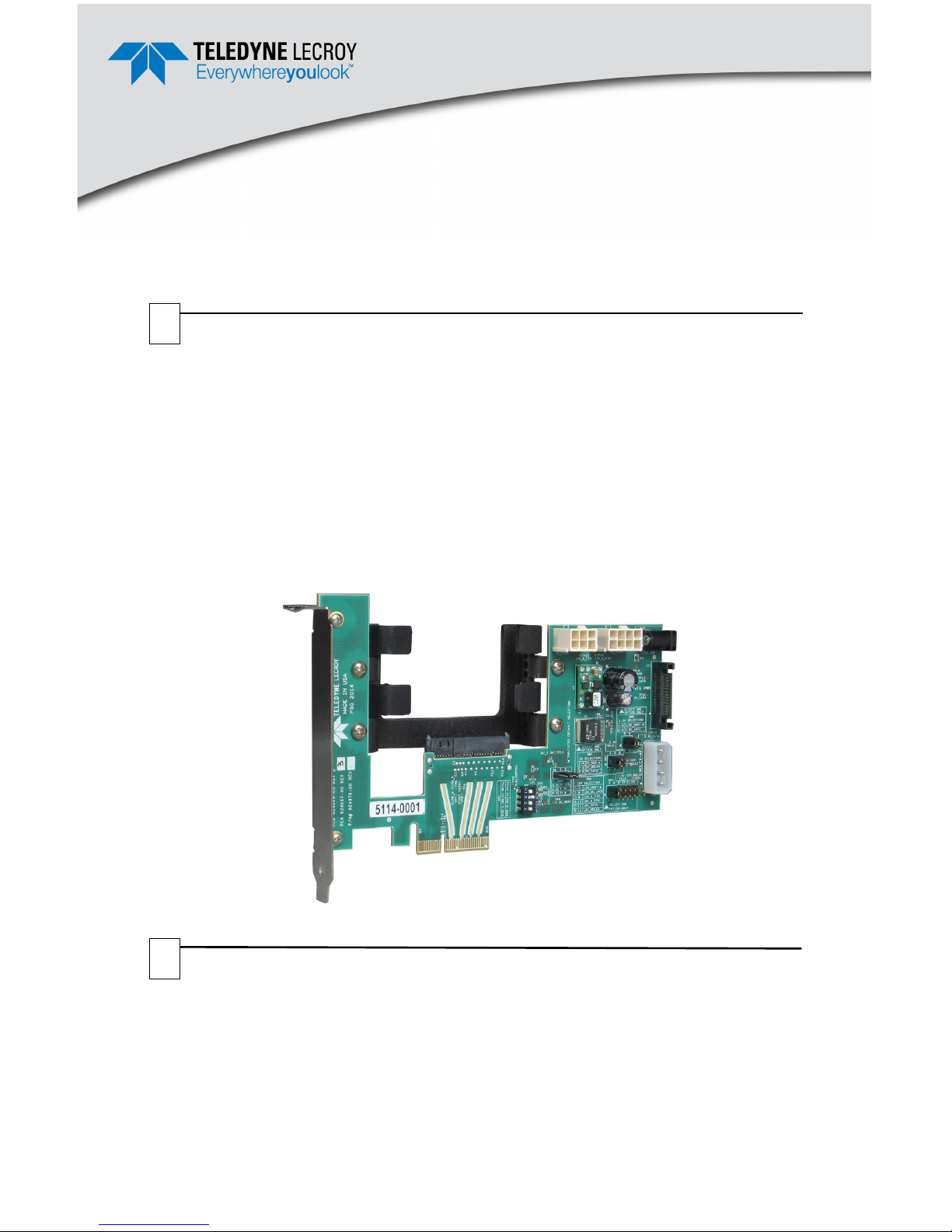
Teledyne LeCroy’s PCIe to SFF-8639 x4 NMVe/SCSIe Port A Adapter card
provides a quick and simple means for test and debug of Solid State Drives (SSDs)
based on PCI Express (PCIe®) protocols. It supports data rates of 2.5 GT/s (Gen1),
5 GT/s (Gen2) and 8 GT/s (Gen3). The PCIe to SFF-8639 x2 NVMe/SCSIe PortB
Adapter looks exactly the same as the Port A adapter except for the silkscreen with
the name of the product. Functionally, the Port B SFF-8639 Adapter works up to X2
since only Lanes 0 and 1 are routed in the PCB from the PCIe edge connector to
the Port B of the SFF-8639 connector.
SFF-8639 Single-Port Adapter Card
1
Components
The adapter package includes the following components:
• SFF-8639 single-port Adapter card
• Power supply +12V @ 3A
• Quick Start Guide (this document)
Inspect the received shipping container for any damage. Unpack the container
and account for each of the system components listed above. Visually inspect
each component for absence of damage.
In the event of damage, notify the shipper and Teledyne LeCroy. Retain all
shipping materials for shipper’s inspection.
2
PCI Express 3.0 to SFF-8639 Adapter
Quick Start
Connections
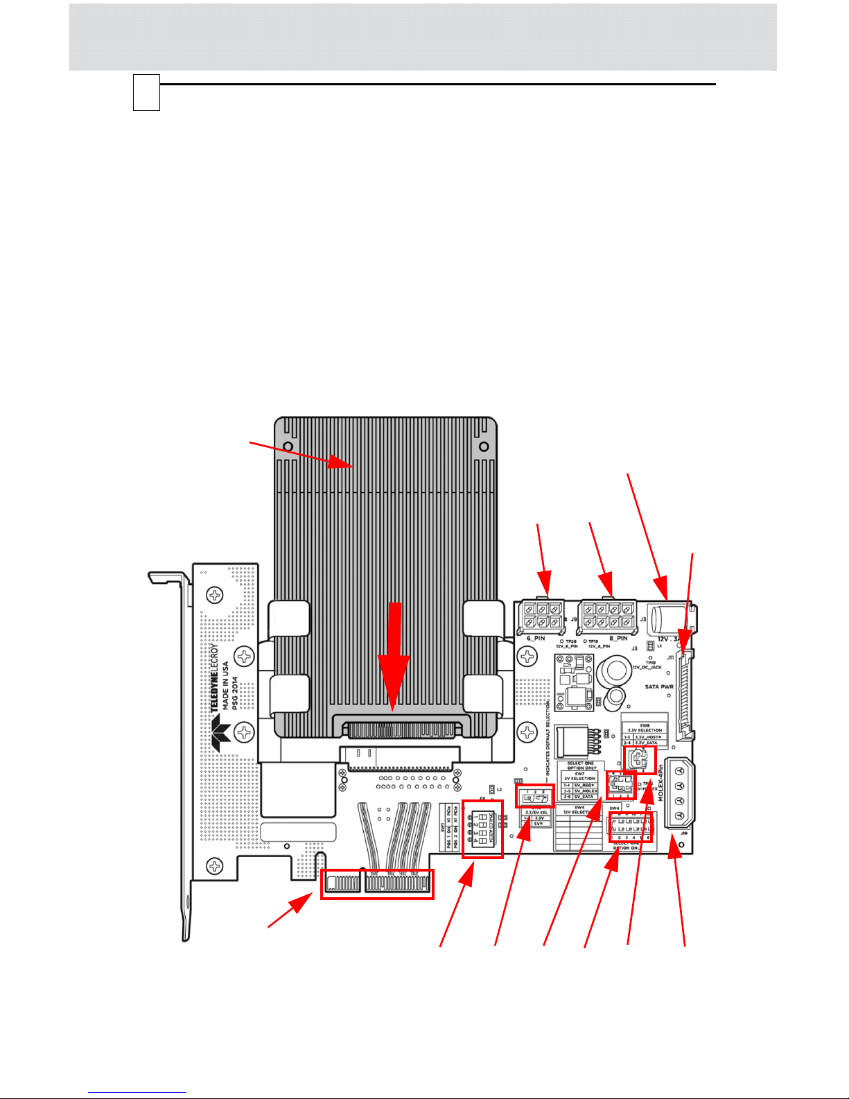
Perform to the following steps to connect the Adapter (see the image below):
1. Insert the SSF-8639 device under test (DUT) through the 2.5" bracket making sure it connects properly in the bottom SSF-8639 connector.
2. Make sure the power for the DUT is sourced correctly using switches SW4,
SW5, SW7, and SW8. The factory default positions are SW1.1 OFF, SW1.2
ON, SW1.3 OFF, SW1.4 OFF, SW4 shunts 1-7, SW5 shunts 2-3, SW7 shunts
1-4, SW8 shunts 1-3. See the tables below to source the correct power for the
DUT.
3. Make sure only switch 2 from the DIP switch array SW1 is in the on position.
The PRSNT# pins configuration is X1 or X4 device is selected using SW1
according to the table.
4. Plug the adapter with the device under test in any PCI Express slot.
5. Connect the power supply to the external power jack (J3) if needed.
PCI Express (PCIe) Interface
(plugs into PCI Express slot)
Device
Under
Tes t
(DUT)
SW1 SW5 SW4
External power jack J3
12V @ 3A minimum
Note: See section 4 for switch
configurations
SW7 SW8
J8 J9
Note: See section 5 for J8 and J9
pin out
J11
J10
3
 Loading...