

TelCom Semiconductor Inc TCN4040E-2.5EZB, TCN4040E-2.5ENB, TCN4040D-2.5EZB, TCN4040D-2.5ENB, TCN4040D-2.5EOA Datasheet
...
PRECISION MICROPOWER
PRELIMINARY INFORMATION
SHUNT VOLTAGE REFERENCE
PRECISION MICROPOWER SHUNT VOLTAGE REFERENCE
TCN4040
TCN4040
FEATURES
■ Small Packages ....... SOT-23B-3, TO-92, and SO-8
■ Output Capacitor Not Required
■ Handles Capacitive Loads
■ Fixed Reverse Breakdown Voltage of 2.5V
■ Low Output Noise
■ Wide Operating Current Range (60µA to 15mA)
■ – 40°C to + 85°C Operating Temperature Range
GENERAL DESCRIPTION
For applications in tight quarters, the TCN4040 precision voltage reference is available in a space-saving
3mm x 1.3mm SOT-23B-3 surface mount package. The
TCN4040 eliminates the need for an external stabilizing
capacitor while maintaining stability with any capacitive
load. The minimum operating current is 60µA. The maximum operating current is 15mA.
To ensure that the prime parts have an accuracy of
APPLICATIONS
■ Portable, Battery-Powered Equipment
■ Data Acquisition Systems
■ Instrumentation
■ Process Control
■ Energy Management
■ Product Testing
■ Automotive
■ Precision Audio Components
better than ±0.5% (C grade) at 25°C, the TCN4040 uses
fuse and zener-zap reverse breakdown voltage trim during
wafer sort. Low dynamic impedance and bandgap reference
temperature drift curvature correction maintain stable reverse breakdown voltage accuracy over a wide range of
operating temperatures (– 40°C to + 85°C) and currents
from (60µA to 15mA).
The TCN4040 also is available in both adjustable and
1.2V versions.
ORDERING INFORMATION
Output Voltage Tolerance
Part No. Voltage (V) Package Temp. Coefficient Grade
TCN4040C-2.5ENB 2.5 SOT-23B-3* ±0.5%, 100ppm/°C Max (C Grade)
TCN4040C-2.5EOA 2.5 8-Pin SOIC ±0.5%, 100ppm/°C Max (C Grade)
TCN4040C-2.5EZB 2.5 TO-92 ±0.5%, 100ppm/°C Max (C Grade)
TCN4040D-2.5EOA 2.5 8-Pin SOIC ±1.0%, 150ppm/°C Max (D Grade)
TCN4040D-2.5ENB 2.5 SOT-23B-3* ±1.0%, 150ppm/°C Max (D Grade)
TCN4040D-2.5EZB 2.5 TO-92 ±1.0%, 150ppm/°C Max (D Grade)
TCN4040E-2.5ENB 2.5 SOT-23B-3* ±2.0%, 150ppm/°C Max (E Grade)
TCN4040E-2.5EZB 2.5 TO-92 ±2.0%, 150ppm/°C Max (E Grade)
NOTE: *SOT-23B-3 is equivalent to the JEDEC (TO-236)
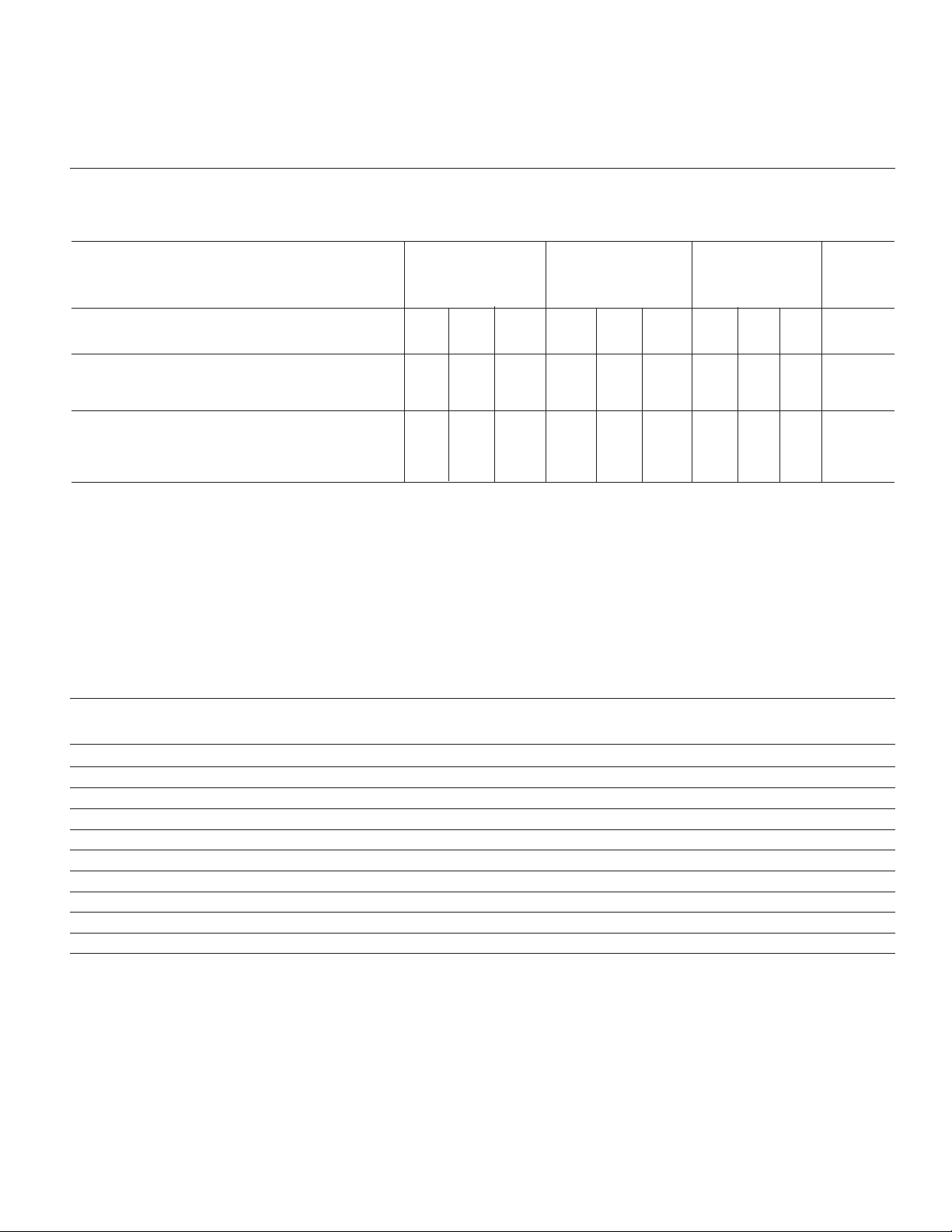
PIN CONFIGURATION
8-Pin SOIC
NC
1
NC
2
3
NC
–
4
NOTE: *SOT-23B-3 is equivalent to the JEDEC (TO-236)
TCN4040-01 6/16/97
TelCom Semiconductor reserves the right to make changes in the circuitry and specifications to its devices.
+
8
NC
7
NC
6
NC
5
TCN4040EOA
SOT-23B-3*
(TOP VIEW)
NC
1
2
+
1
3
–
TCN4040ENB
NC
+
TO-92-3
123
TCN4040EZB
–
PRELIMINARY INFORMATION
TCN4040
PRECISION MICROPOWER
SHUNT VOLTAGE REFERENCE
ABSOLUTE MAXIMUM RATINGS* (Note 1)
Reverse Current.......................................................20mA
Forward Current .......................................................10mA
Power Dissipation (TA = 25°C) (Note 2)
SOT-23B-3 Package ......................................230mW
ESD Susceptibility
Human Body Model (Note 3) ................................2kV
Machine Model (Note 3) .....................................200V
*Functional operation above the absolute maximum stress rating is not
implied.
TO-92 Package ..............................................440mW
SO-8 Package ................................................470mW
Storage Temperature ...........................– 65°C to + 150°C
Lead Temperature (Soldering, 10 seconds)
EOA ................................................................+260°C
ENB ................................................................+300°C
EZB.................................................................+300°C
NOTES: 1. Absolute Maximum Ratings indicate limits beyond which damage to the device may occur. Operating Ratings indicate conditions for which
the device is functional, but do not guarantee specific performance limits. For guaranteed specifications and test conditions, see
Characteristics.
the device is not operated under the listed test conditions.
2. The maximum power dissipation must be derated at elevated temperatures and is dictated by T
(junction to ambient thermal resistance), and TA (ambient temperature). The maximum allowable power dissipation at any temperature is
PD
= (T
MAX
the typical thermal resistance (θJA), when board mounted, is 185°C/W for the M package, 326°C/W for the SOT-23B-3 package, and 180°
C/W with 0.4” lead length and 170°C/W with 0.125” lead length for the TO-92-3 package.
3. The human body model is a 100pF capacitor discharged through a 1.5kΩ resistor into each pin. The machine model is a 200pF capacitor
discharged directly into each pin.
ELECTRICAL CHARACTERISTICS:
The guaranteed specifications apply only for the test conditions listed. Some performance characteristics may degrade when
J
MAX
– TA) /θ
or the number given in Absolute Maximum Ratings, whichever is lower. For the TCN4040, T
JA
Boldface type specifications apply for TA = TJ = T
tions; T
= TJ = 25°C.
A
OPERATING RATINGS (NOTES 1 AND 2)
Temperature Range
(T
≤ TA ≤ T
MIN
Reverse Current
TCN4040-2.5 ...................................... .60µA to 15mA
) .....................– 40°C ≤ TA ≤ +85°C
MAX
(maximum junction temperature), θ
J
MAX
= 125°C, and
J
MAX
MIN
to T
. All other specifica-
MAX
Electrical
JA
TCN4040CEOA TCN4040DEOA TCN4040EENB
TCN4040CENB TCN4040DENB TCN4040EEZB
TCN4040CEZB TCN4040DEZB
Symbol Parameter Test Min Typ Max Min Typ Max Min Typ Max Unit
Conditions
V
R
I
R
MIN
∆VR/∆T Average Reverse IR =10mA — ±20 ±100 — ±20 ±150 — ±20 ±150 ppm/°C
∆V
R
Z
R
Reverse Breakdown
IR =100µA — 2.500 — — 2.500 — — 2.500 — V
Voltage Notes 4, 5
Reverse Breakdown IR =100µA— ±12 — ±25 — — ±50 mV
Voltage Tolerance Notes 4, 5, 6 — ±29 — ±49 — ±74
Minimum Operating Notes 4, 5 — 45 60 — 45 65 — 45 65 µA
Current — 65 — 70 — 70
Breakdown Voltage I
Temperature I
=1mA ±15 ±15 ±15
R
=100µA ±15 ±15 ±15
R
Coefficient Notes 4, 5
/∆IRReverse Breakdown I
≤ IR ≤ 1mA
R
MIN
— 0.4 0.8 — 0.4 1.0 — 0.4 1.0 mV
Voltage Change with Notes 4, 5 — 1.0 — 1.2 — 1.2
Operating Current
Change
1mA ≤ IR =12mA
— 2.3 6.0 — 2.3 8.0 — 2.3 8.0 mV
— 8.0 — 10.0 — 10.0
Reverse Dynamic
Impedance I
IR =1mA, f = 120Hz,
= 0.1 I
AC
R
— 0.3 0.9 — 0.3 1.1 — 0.3 1.1 Ω
Notes 4, 5
TCN4040-01 6/16/97
2
PRECISION MICROPOWER
SHUNT VOLTAGE REFERENCE
PRELIMINARY INFORMATION
TCN4040
ELECTRICAL CHARACTERISTICS (Cont.):
Boldface type specifications apply for TA = TJ = T
specifications; TA = TJ = 25°C.
MIN
to T
MAX
. All other
TCN4040CEOA TCN4040DEOA TCN4040EENB
TCN4040CENB TCN4040DENB TCN4040EEZB
TCN4040CEZB TCN4040DEZB
Symbol Parameter Test Min Typ Max Min Typ Max Min Typ Max Unit
Conditions
e
N
∆V
R
NOTES: 4. Typicals are at TJ = 25°C and represent most likely parametric norm.
Wideband Noise IR =100µA, — 35— —35— —35— µVmsec
10Hz ≤ f ≤ 10kHz
Notes 4, 5
Reverse Breakdown t =1000hrs — 120 — — 120 — — 120 — ppm/°C
Voltage Long Term T = 25°C ±0.1°C
Stability I
5. Limits are 100% production tested at 25°C.
6. The boldface (over-temperature) limit for Reverse Breakdown Voltage Tolerance is defined as the room temperature Reverse Breakdown
Voltage Tolerance ±[(∆VR/∆T)(65°C)(VR)]. ∆VR/∆T is the VR temperature coefficient, 65°C is the temperature range from – 40°C to the
reference point of 25°C, and VR is the reverse breakdown voltage. The total over-temperature tolerance for the different grades is shown
below:
C-grade: ±1.15% = ±0.5% ±100ppm/°C x 65°C
D-grade: ±1.98% = ±1.0% ±150ppm/°C x 65°C
E-grade: ±2.98% = ±2.0% ±150ppm/°C x 65°C
=100µA
R
Notes 4, 5
PIN DESCRIPTION
Pin No. Pin No. Pin No.
(SOT-23B-3) TO-92 8-Pin SOIC Symbol Description
1 1 1 NC No connection
2 NC No connection
3 NC No connection
2 2 + Positive terminal
3 3 – Negative terminal
4 – Negative terminal
5 NC No connection
6 NC No connection
7 NC No connection
8 + Positive terminal
TCN4040-01 6/16/97
3
 Loading...