

TelCom Semiconductor Inc TCM853EOA, TCM853COA, TCM852EOA, TCM852COA, TCM851COA Datasheet
...
REGULATED GaAs FET BIAS SUPPLY
EVALUATION
KIT
AVAILABLE
TCM850
TCM851
TCM852
TCM853
1
FEATURES
■ Fixed – 4.1V or Adjustable – 0.5V to – 9V Output
at 5mA
■ 4.5V to 10V Input Voltage Range
■ Low Output Voltage Ripple
TCM850-852 ..............................................2mVp-p
TCM853......................................................1mVp-p
■ 100kHz Charge Pump Switching Frequency
■ Optional External Synchronizing Clock
Input (TCM852)
■ Logic Level Shutdown Mode ................ 0.5µA Typ.
Temperature (TCM850/852/853)
■ Low Cost, 8-Pin SOIC Package
APPLICATIONS
■ Cellular Phones
■ Negative Regulated Power Supplies
■ LCD Bias Contrast Control
■ Adjustable GaAs FET Bias
■ Wireless Data Loggers
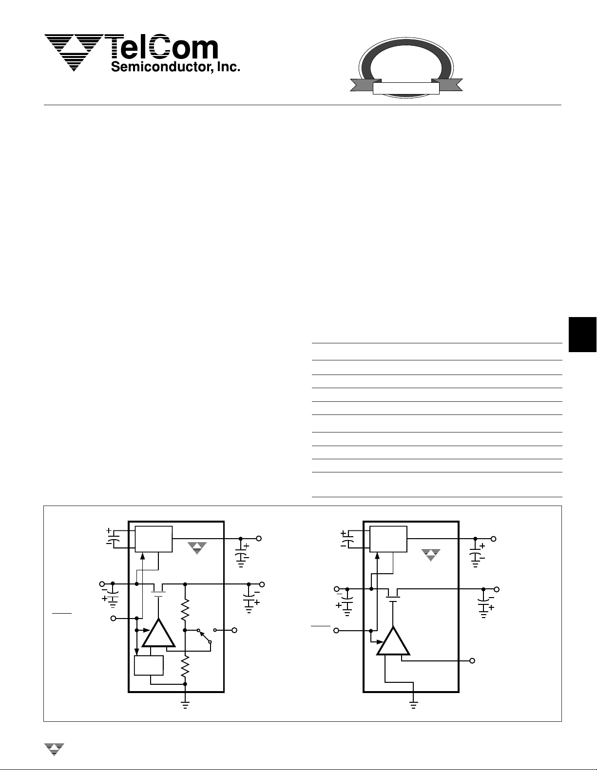
FUNCTIONAL BLOCK DIAGRAM
GENERAL DESCRIPTION
The TCM850/1/2/3 combines an inverting charge pump
and a low noise linear regulator in a single small outline
package. They are ideal for biasing GaAS FETs in cellular
telephone transmitter power amplifiers
All four devices accept a range of input voltages from
4.5V to 10.0V and have – 5mA output current capability. The
TCM850/1/2 have both preset (– 4.1V) and variable (– 0.5V
to –9.0V) output voltages that program with an external
resistor divider. The TCM853 output voltage programs with
an external positive control voltage. The TCM850/1/3 can
be shutdown reducing quiescent current to less than
0.5µA (typ) over temperature, 2µA (typ) for the TCM851.
ORDERING INFORMATION
Part No. Package Temp. Range
TCM850COA 8-Pin SOIC 0°C to +70°C
TCM850EOA 8-Pin SOIC – 40°C to +85°C
TCM851COA 8-Pin SOIC 0°C to +70°C
TCM851EOA 8-Pin SOIC – 40°C to +85°C
TCM852COA 8-Pin SOIC 0°C to +70°C
TCM852EOA 8-Pin SOIC – 40°C to +85°C
TCM853COA 8-Pin SOIC 0°C to +70°C
TCM853EOA 8-Pin SOIC – 40°C to +85°C
TCM850EV Evaluation Kit for
TCM850/1/2/3
2
3
4
5
NEGOUT
SHDN (TCM850)
SHDN (TCM851)
OSC (TCM852)
TELCOM SEMICONDUCTOR, INC.
+
C1
C1
–
CHARGE
PUMP
N
+
– 1.28V
REF
–
TCM850
TCM851
TCM852
GND
IN
C
3
OUT
C4
FB
(GND to SET
= – 4.1V)
V
OUT
C
SHDN
Figure 1.
C
1
C
2
+
C1
C1
–
CHARGE
PUMP
N
TCM853
IN
C
3
OUTNEGOUT
C
4
C
1
2
6
7
+
–
CONT
(CONTROL VOLTAGE)
GND
TC850/1/2/3-3 10/1/96
4-27
8
TCM850
TCM851
TCM852
TCM853
REGULATED GaAs FET BIAS SUPPLY
ABSOLUTE MAXIMUM RATINGS*
Supply Voltage (V
V
NEGOUT
VIN to V
V
OUT
to GND ...................................... – 10.5V to 0.3V
NEGOUT
to GND** ........................................ V
SHDN or OSC (Pin 4) to GND ........– 0.3V to (V
to GND).................. – 0.3V to +10.5V
IN
...............................................................– 0.3 to 21V
NEGOUT
to 0.3V
+ 0.3V)
IN
*This is a stress ratings only and functional operation of the device at these
or any other conditions above those indicated in the operational sections of
the specifications is not implied. Exposure to Absolute Maximum Rating
Conditions for extended periods may affect device reliability.
**The output may be shorted to NEGOUT or GND if the package power
dissipation is not exceeded. Typical short circuit current to GND is 50mA.
Power Dissipation (TA < 70°C)
SOIC ...........................................................470mW
Operating Temperature Range
C Device ..............................................0°C to 70°C
E Device ....................................... – 40°C to +85°C
Storage Temperature Range ................– 65°C to +165°C
Lead Temperature (Soldering, 10 sec) .................+300°C
ELECTRICAL CHARACTERISTICS: V
between +5V and +10V; V
IN
T
unless otherwise noted. A 100kHz, 50% duty cycle square wave
MAX
= – 4.1V; RL = Open Circuit; TA = T
OUT
MIN
between GND and VIN is applied to the OSC pin of the TCM852.
Symbol Parameter Test Conditions Min Typ Max Unit
V
IN
V
OUT
V
FBSET
I
Q
I
SHUT
f
OSC
V
IH
V
IL
I
IN
C
IN
NOTES: 1. The supply voltage can drop to 4.5V, but the output is no longer guaranteed to sink 5mA at – 4.1V.
Supply Voltage Note 1 5 — 10 V
Output Voltage TCM850-TCM852: VFB = 0V (Note 3) – 4.3 – 4.1 – 3.9 V
TCM853: V
Output Voltage Range
= 4.1V – 4.2 — – 4
CTRL
– 0.5 to – (V
–1)
IN
Set Voltage TCM850-852: No Load – 1.32 – 1.28 – 1.24 V
Supply Current — 2 3 mA
Shutdown Supply Current TCM850/853: VIN = 10V, SHDN = 0V — 0.5 — µA
TCM851: SHDN = 2V — 2 —
TCM852: OSC Low — 0.5 —
V
Load Regulation TCM850-TCM852: V
OUT
TCM853: V
V
Ripple TCM850-TCM852 — 2 — mVp-p
OUT
CTRL
= 0V (Note 3) — 4 8 mV/mA
FB
= 4.1V — 3 8
TCM853 — 1 —
Oscillator Frequency TCM850-TCM853: TA = 25°C (Note 2) 80 100 120 kHz
Input High Voltage Pin 4 2 — — V
Input Low Voltage Pin 4 — — 0.5 V
Input Current Pin 4 — — ±1 µA
Input Capacitance Pin 4 — 10 — pF
2. The TCM852 will operate with a 50kHz to 250kHz square wave of 40% to 60% duty cycle. For best performance, use an 80kHz to
120kHz square wave with 50% duty cycle.
3. I
= 0mA or 5mA. Reference Figures 3 and 5.
OUT
V
to
4-28
TELCOM SEMICONDUCTOR, INC.

REGULATED GaAs FET BIAS SUPPLY
PIN CONFIGURATIONS
TCM850
TCM851
TCM852
TCM853
1
8-Pin SOIC
C1
C1
NEGOUT
SHDN
+
–
1
2
TCM850COA
3
TCM850EOA
4
8
IN
7
GND
6
OUT
FB
5
C1
C1
NEGOUT
SHDN
+
–
1
2
TCM851COA
3
TCM851EOA
4
8
7
6
5
IN
GND
NEGOUT
OUT
FB
Figure 2.
C1
C1
OSC
+
–
1
2
TCM852COA
3
TCM852EOA
4
IN
8
7
GND
6
OUT
FB
5
C1
C1
NEGOUT
SHDN
+
–
1
2
TCM853COA
3
TCM853EOA
4
PIN DESCRIPTION
Pin No Pin No Pin No Pin No
(TCM850) (TCM851) (TCM852) (TCM853) Symbol Description
11 11C
22 22C
3 3 3 3 NEGOUT Negative (unregulated) output voltage.
4 — — 4 SHDN Shutdown input (TTL active LOW).
— 4 — — SHDN Shutdown input (TTL active HIGH).
— — 4 — OSC External oscillator input.
5 5 5 — FB Feedback input. OUT is preset to – 4.1V when FB is
— — — 5 CONT Control input. V
6 6 6 6 OUT Output voltage terminal.
7 7 7 7 GND Ground.
8 8 8 8 IN Positive power supply input voltage (4.5V to 10V).
+
1
–
1
C1 positive input terminal.
C1 negative input terminal.
grounded. OUT may be adjusted to other voltages by
connecting a resistor divider as shown in Figure 4.
is adjusted with a positive control
voltage (0V to 10V) applied to this input through a resistive
divider (Figure 5).
OUT
2
8
IN
7
GND
OUT
6
CONT
5
3
4
5
TELCOM SEMICONDUCTOR, INC.
6
7
8
4-29
 Loading...