

TelCom Semiconductor Inc TCM810TENB, TCM810RENB, TCM810SENB, TCM810MENB, TCM810LENB Datasheet
...
3-PIN µP RESET MONITORS
FEATURES
PRELIMINARY INFORMATION
1
TCM809
TCM810
2
GENERAL DESCRIPTION
■ Precision VCC Monitor for 3.0V, 3.3V, 5.0V
Nominal System V Supplies
■ 140msec Guaranteed Minimum RESET, RESET
Output Duration
■
RESET Output Guaranteed to VCC = 1.0V (TCM809)
■ Low 17µA Supply Current
■ VCC Transient Immunity
■ Small SOT-23B-3 Package
■ No External Components
TYPICAL APPLICATIONS
■ Computers
■ Embedded Systems
■ Battery Powered Equipment
■ Critical µP Power Supply Monitoring
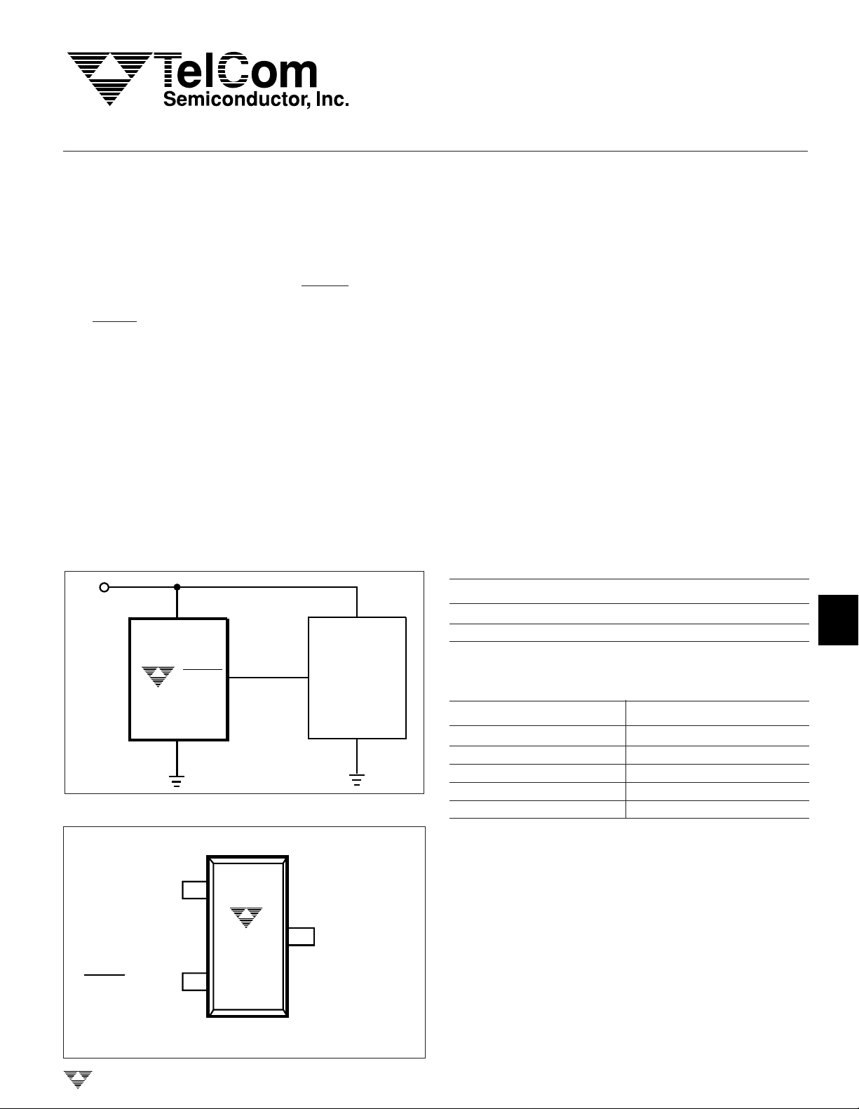
TYPICAL OPERATING CIRCUIT
V
CC
V
CC
V
CC
PROCESSOR
The TCM809 and TCM810 are cost-effective system
supervisor circuits designed to monitor VCC in digital systems and provide a reset signal to the host processor when
necessary. No external components are required.
The reset output is driven active within 20msec of V
falling through the reset voltage threshold. Reset is maintained active for a minimum of 140msec after VCC rises
above the reset threshold. The TCM810 has an active-high
reset output while the TCM809 has an active-low reset
output. The output of the TCM809 is guaranteed valid down
to VCC = 1V. Both devices are available in a
SOT-23B-3 package.
The TCM809/810 are optimized to reject fast transient
glitches on the VCC line. Low supply current of 17µA
(V
= 3.3V) makes these devices suitable for battery
CC
powered applications.
CC
ORDERING INFORMATION
Part No. Package Temp. Range
T
CM809xENB SOT-23B-3 – 40°C to +85 °C
TCM810xENB SOT-23B-3 – 40°C to +85 °C
NOTE: The "X" denotes a suffix for VCC threshold - see table below.
3
4
5
RESET
TCM809
GND
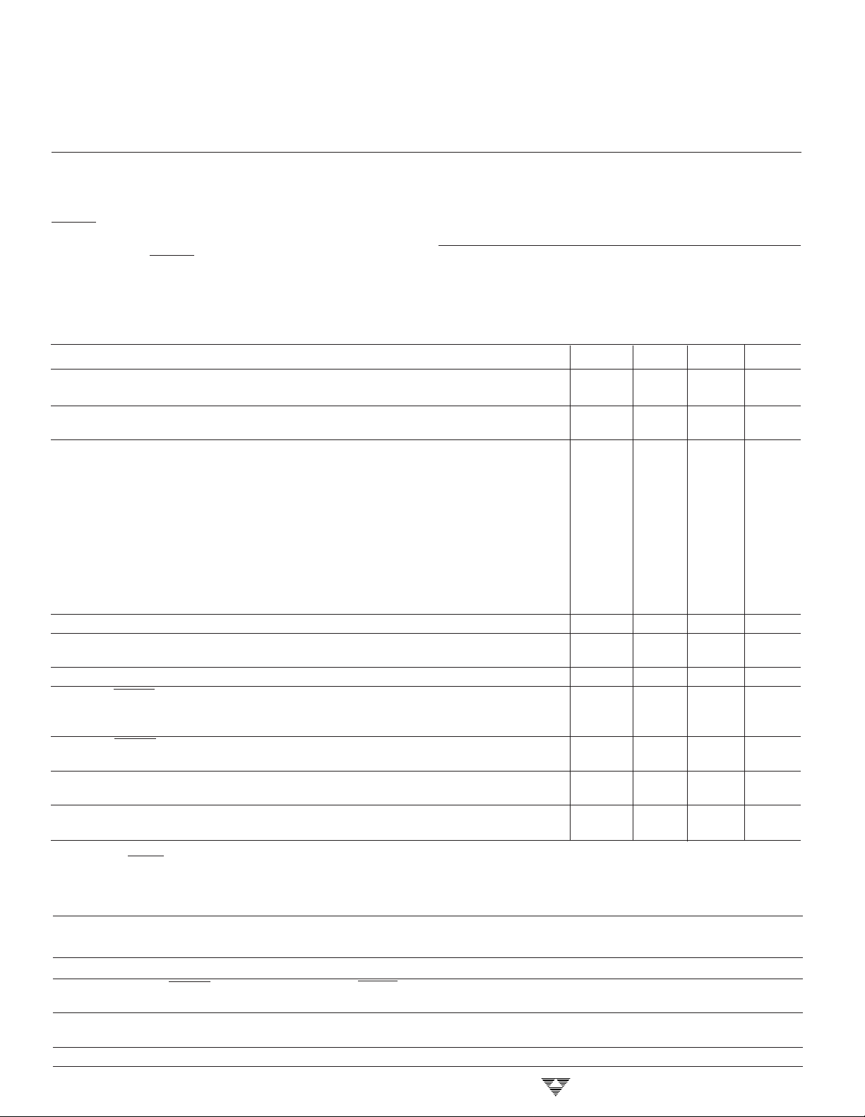
PIN CONFIGURATION
*SOT-23B-3
1
GND
TCM809xENB
TCM810xENB
RESET (RESET)
NOTE: *SOT-23B-3 is equivalent to JEDEC (TO-236)
** () is for TCM810
TELCOM SEMICONDUCTOR, INC.
2
3
RESET
INPUT
V
CC
GND
Suffix Reset VCC Threshold (V)
L
M 4.38
T 3.08
S 2.93
R 2.63
4.63
TCM809/810-04 8/29/96
5-15
6
7
8
PRELIMINARY INFORMATION
TCM809
TCM810
3-PIN µP RESET MONITORS
ABSOLUTE MAXIMUM RATINGS*
Supply Voltage (V
RESET, RESET ............................ – 0.3V to (VCC + 0.3V)
Input Current, VCC....................................................20mA
Output Current, RESET, RESET .............................20mA
dV/dt (VCC) .......................................................... 100V/µS
Operating Temperature Range ...............– 40°C to +85°C
ELECTRICAL CHARACTERISTICS: V
to GND) ................................ +6.0V
CC
cc
= 5V, TA = Operating Temperature Range unless otherwise noted.
Power Dissipation (TA ≤ 70°C)
SOT-23B-3 (derate 4mW/°C above +70°C) ...230mW
Storage Temperature Range ................– 65°C to +150°C
Lead Temperature (Soldering, 10 sec) .................+260°C
*This is a stress rating only and functional operation of the device at these
or any other conditions above those indicated in the operational sections of
the specifications is not implied. Exposure to Absolute Maximum Rating
Conditions for extended periods may affect device reliability.
Symbol Parameter Test Conditions Min Typ Max Unit
VCC Range TA = 0°C to +70°C 1.0 — 5.5 V
TA = – 40°C to +85°C 1.2 — 5.5
I
CC
V
TH
V
OL
V
OH
V
OL
V
OH
NOTES: 1. Production testing done at TA = +25°C, over temperature limits guaranteed by design.
Supply Current TCM8xxL/M: VCC < 5.5V — 24 60 µA
TCM8xxR/S/T: VCC < 3.6V — 17 50
Reset Threshold (Note 2)
TCM8xxL: T
= – 40°C to +85°C 4.50 — 4.75
T
A
TCM8xxM: T
= – 40°C to +85°C 4.25 — 4.50
T
A
TCM8xxT: T
T
= – 40°C to +85°C 3.00 — 3.15
A
TCM8xxS: T
= – 40°C to +85°C 2.85 — 3.00
T
A
TCM8xxR: T
= +25°C 4.56 4.63 4.70 V
A
= +25°C 4.31 4.38 4.45
A
= +25°C 3.04 3.08 3.11
A
= +25°C 2.89 2.93 2.96
A
= +25°C 2.59 2.63 2.66
A
TA = – 40°C to +85°C 2.55 — 2.70
Reset Threshold Tempco — 30 — ppm/°C
VCC to Reset Delay (Note 2)
VCC = VTH to (VTH – 100mV) — 20 — µsec
Reset Active Timeout Period 140 240 560 msec
RESET Output Voltage Low TCM809R/S/T: VCC = VTH min, I
(TCM809) TCM809L/M: V
VCC > 1.0V, I
RESET Output Voltage High
(TCM809)
RESET Output Voltage Low
(TCM810)
TCM809R/S/T: VCC > VTH max, I
TCM809L/M: VCC > VTH max, I
T
CM810R/S/T: VCC = VTH max, I
T
CM810L/M: VCC = VTH max, I
RESET Output Voltage High 1.8 < VCC < VTH min, I
= VTH min, I
CC
SOURCE
SINK
= 1.2mA — — 0.3 V
SINK
= 3.2mA — — 0.4
SINK
= 50µA — — 0.3
= 500µA 0.8 V
SOURCE
= 800µAVCC – 1.5 — —
SOURCE
= 1.2mA — — 0.3 V
SINK
= 3.2mA — — 0.4
SINK
= 150µA 0.8 V
CC
CC
——V
——V
(TCM810)
2. RESET output for TCM809, RESET Output for TCM810.
PIN DESCRIPTION
Pin No.
(SOT-23B-3) Symbol Description
1 GND Ground
2 RESET (TCM809) RESET output remains low while V
for 240msec (140msec min.) after VCC rises above reset threshold.
2 RESET (TCM810) RESET output remains high while VCC is below the reset voltage threshold,
and for 240msec (140msec min.) after VCC rises above reset threshold.
3VCCSupply voltage (Typ. +3.0V to +5.0V)
5-16
is below the reset voltage threshold, and
CC
TELCOM SEMICONDUCTOR, INC.
 Loading...