

TelCom Semiconductor Inc TCM680EPA, TCM680CPA, TCM680EOA, TCM680COA Datasheet
+5V TO ± 10V VOL T AGE CONVERTER
FEATURES
EV ALUATION
KIT
A V AILABLE
GENERAL DESCRIPTION
1
TCM680
2
■ 99% Voltage Conversion Efficiency
■ 85% Power Conversion Efficiency
■ Wide Voltage Range .........................+2.0V to +5.5V
■ Only 4 External Capacitors Required
■ Space Saving 8-Pin SOIC Design
APPLICATIONS
■ ±10V From +5V Logic Supply
■ ±6V From a 3V Lithium Cell
■ Handheld Instruments
■ Portable Cellular Phones
■ LCD Display Bias Generator
■ Panel Meters
■ Operational Amplifier Power Supplies
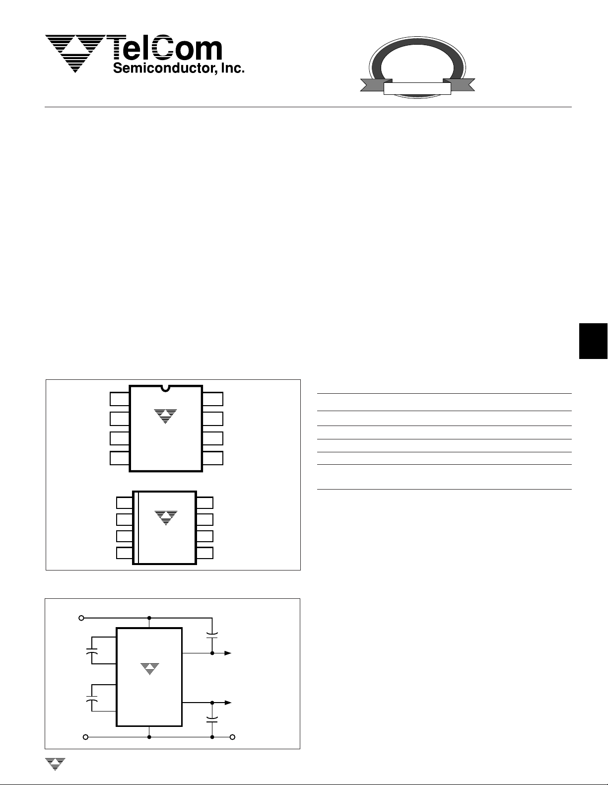
PIN CONFIGURATIONS (DIP AND SOIC)
8
7
6
5
V
C
V
GND
+
V
OUT
+
C
1
V
IN
GND
+
OUT
+
1
IN
V
C
C
C
–
OUT
V
–
1
1
+
2
2
–
2
C
C
C
–
OUT
–
1
+
2
–
2
TCM680CPA
3
TCM680EPA
4
18
2
TCM680COA
3
TCM680EOA
4
7
6
5
The TCM680 is a dual charge pump voltage converter
that develops output voltages of +2VIN and – 2VIN from a
single input voltage of +2.0V to +5.5V. Common applications include ±10V from a single +5V logic supply, and ±6V
from a +3V lithium battery.
The TCM680 is packaged in a space-saving 8-pin
SOIC package and requires only four inexpensive external
capacitors. The charge pumps are clocked by an on-board
8kHz oscillator. Low output source impedances (typically
150Ω) provides maximum output currents of 10mA for each
output. Typical power conversion efficiency is 85%.
High efficiency, small installed size and low cost make
the TCM680 suitable for a wide variety of applications that
need both positive and negative power supplies derived
from a single input voltage.
ORDERING INFORMATION
Part No. Package Temperature
TCM680COA 8-Pin SOIC 0°C to +70°C
TCM680CPA 8-Pin Plastic DIP 0°C to +70°C
TCM680EOA 8-Pin SOIC – 40°C to +85°C
TCM680EPA 8-Pin Plastic DIP – 40°C to +85°C
TC7660EV Charge Pump Family
Evaluation Kit
3
4
5
6
TYPICAL OPERATING CIRCUIT
+5V
C1
4.7µF
C2
4.7µF
GND
2.0V<V
+
+
C
C
C
C
+
1
–
1
+
TCM680
2
–
2
IN
V
IN
GND
< +5.5V
+
V
OUT
–
V
OUT
TELCOM SEMICONDUCTOR, INC.
4.7µFC4
+
+
V
OUT
–
V
OUT
4.7µF
C3
+
GND
7
= (2xVIN)
= (– 2 x VIN)
8
TC660-2 9/4/96
4-13
TCM680
C
1
C
1
C
2
C
3
C
2
V
IN
V
IN
V
OUT
V
OUT
V
OUT
GND
GND
TCM680
4.7µF
4.7µF
10µF
C
4
10µF
8
7
6
54
3
2
1
V
OUT
C
2
R
L
R
L
C
1
–
+
–
–
+
+
+
–
+
–
+5V TO
±10V VOLT AGE CONVERTER
ABSOLUTE MAXIMUM RATINGS*
V
.....................................................................................................+6.0V
IN
+
V
.............................................................................................. +12.0V
OUT
–
V
.............................................................................................– 12.0V
OUT
–
V
Short-Circuit Duration ............................Continuous
OUT
+
V
Current ............................................................75mA
OUT
V
dV/dT.............................................................. 1V/µsec
IN
Power Dissipation (TA ≤ 70°C)
Plastic DIP ......................................................730mW
Small Outline ..................................................470mW
Storage Temperature ............................– 65°C to +150°C
Lead Temperature (Soldering, 10 sec) .................+300°C
*Stresses above those listed in "Absolute Maximum Ratings" may cause
permanent damage to the device. These are stress ratings only and
functional operation of the device at these or other conditions above those
indicated in the operation section of the specification is not implied.
Exposure to the Absolute Maximum Ratings conditions for extended
periods of time may affect device reliability.
ELECTRICAL CHARACTERISTICS: V
= +5V, TA = +25°C, test circuit Figure 1, unless otherwise indicated.
IN
Symbol Parameter Test Conditions Min Typ Max Unit
Supply Voltage Range MIN. ≤ TA ≤ MAX., RL = 2kΩ 2.0 1.5 to 5.5 5.5 V
Supply Current VIN = 3V, RL = ∞ — 0.5 1 mA
= 5V, RL = ∞ —1 2
V
IN
V
= 5V, 0°C ≤ TA ≤ +70°C, RL = ∞ — — 2.5
IN
VIN = 5V, – 40°C ≤ TA ≤ +85°C, RL = ∞ ——3
Negative Charge Pump Output I
Source Resistance I
–
= 10mA, I
L
–
= 5mA, I
L
–
= 10mA, I
I
L
0°C ≤ T
– 40°C ≤ TA ≤ +85°C — — 250
Positive Charge Pump Output I
Source Resistance I
+
= 10mA, I
L
+
= 5mA, I
L
+
I
= 10mA, I
L
0°C ≤ T
– 40°C ≤ TA ≤ +85°C — — 250
F
OSC
P
EFF
V
OUT EFF
TelCom Semiconductor reserves the right to make changes in the circuitry or specifications detailed in this manual at any time without notice. Minimums
and maximums are guaranteed. All other specifications are intended as guidelines only. TelCom Semiconductor assumes no responsibility for the use of
any circuits described herein and makes no representations that they are free from patent infringement.
Oscillator Frequency — 21 — kHz
Power Efficiency RL = 2kΩ —85—%
V
+
OUT
–
OUT
Voltage Conversion Efficiency V
+
= 0mA, VIN = 5V — 140 180 Ω
L
+
= 0mA, VIN = 2.8V — 180 250
L
+
= 0mA, VIN = 5V:
L
≤ +70°C — — 220
A
–
= 0mA, VIN = 5V — 140 180 Ω
L
–
= 0mA, VIN = 2.8V — 180 250
L
–
= 0mA, VIN = 5V:
L
≤ +70°C — — 220
A
, RL = ∞ 97 99 — %
, RL = ∞ 97 99 —
PIN DESCRIPTION
8-Pin
DIP/SOIC
1C
2C
3C
4V
5 GND Input. Device ground.
6VINInput. Power supply voltage.
7C
8V
4-14
Symbol Description
–
1
+
2
–
2
–
OUT
+
1
+
OUT
Input. Capacitor C1 negative terminal.
Input. Capacitor C2 positive terminal.
Input. Capacitor C2 negative terminal.
Output. Negative output voltage (–2VIN).
Input. Capacitor C1 positive terminal.
Output. Positive output voltage (+2VIN)
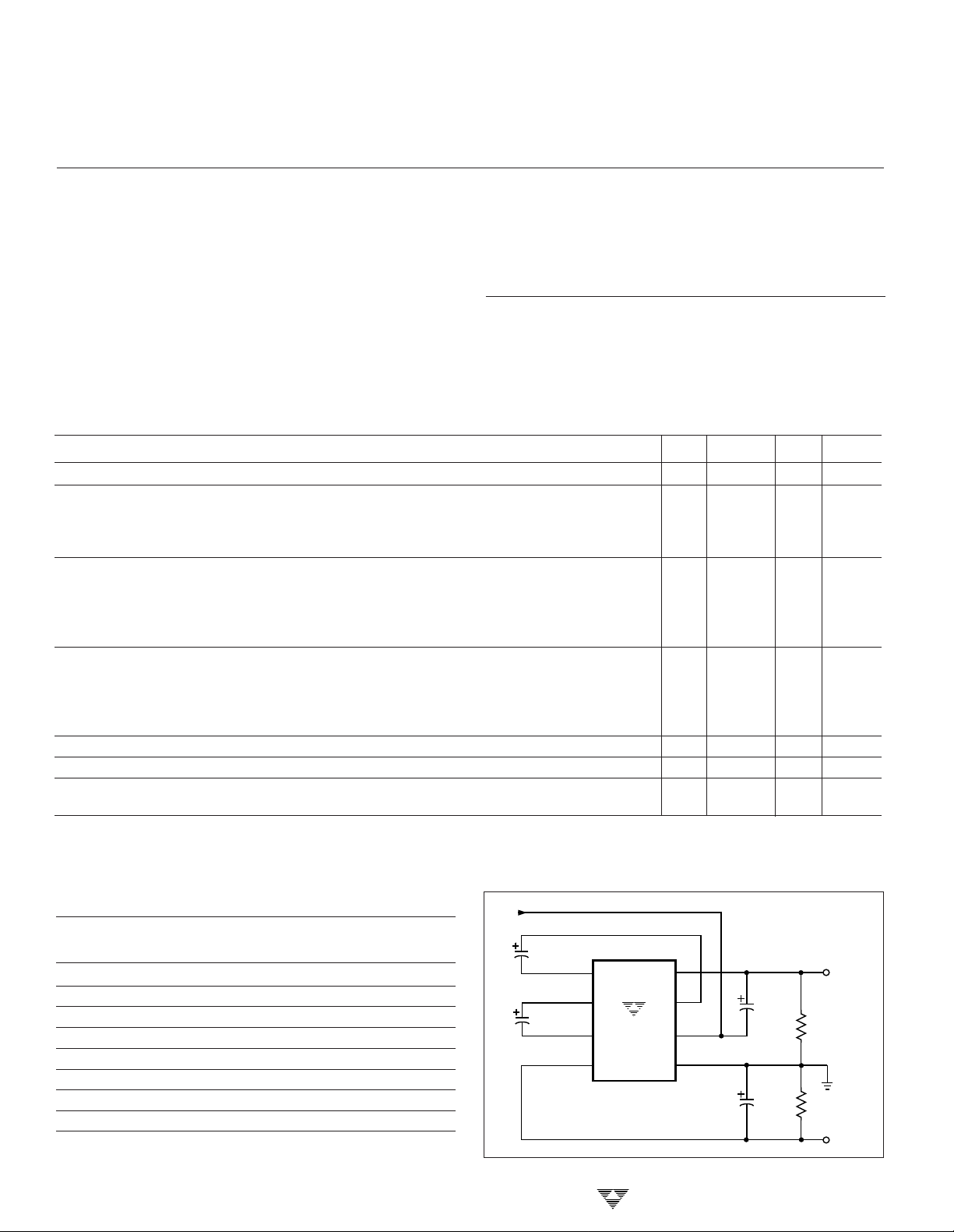
Figure 1. Test Circuit
TELCOM SEMICONDUCTOR, INC.
+5V TO
±10V VOLT AGE CONVERTER
1
TCM680
DETAILED DESCRIPTION
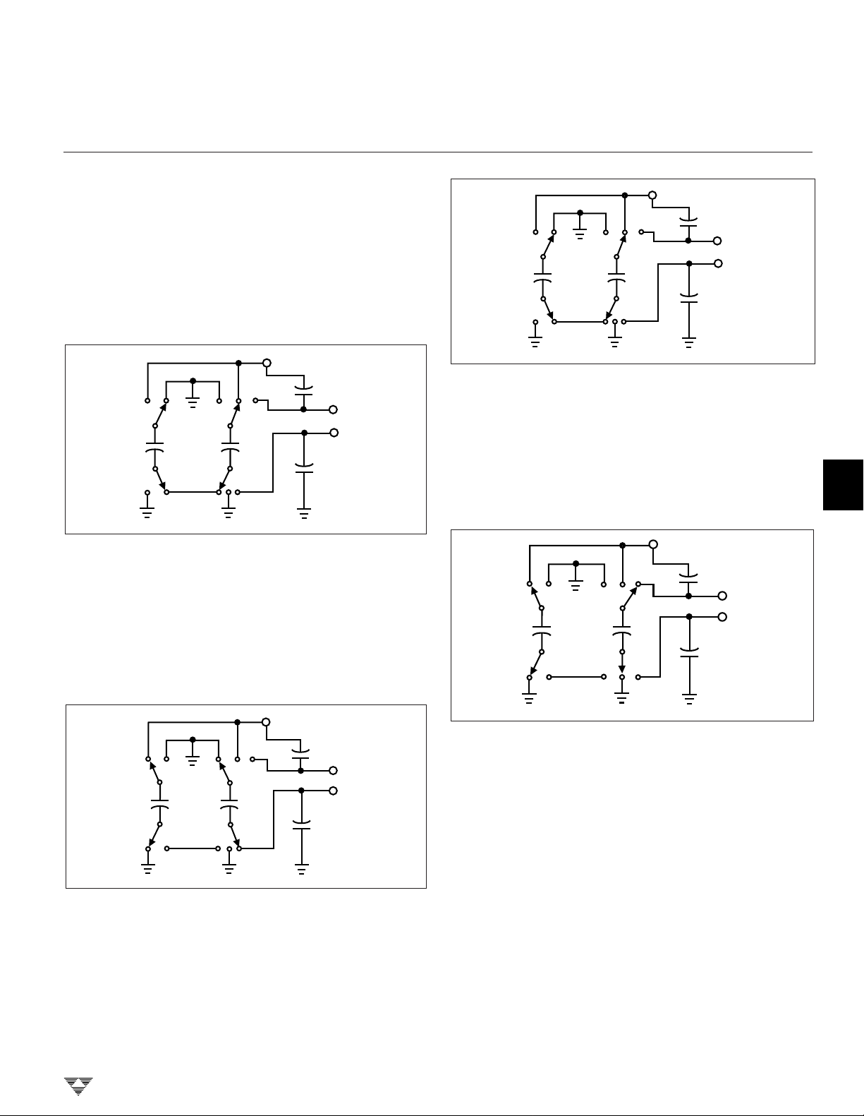
Phase 1
VSS charge storage – The positive side of capacitors C
and C2 are connected to +5V at the start of this phase. C
then switched to ground and the charge in C
to C
–
. Since C
2
+
is connected to +5V, the voltage potential
2
–
is transferred
1
across capacitor C2 is now 10V.
V
= +5V
IN
–
C
4
+
V
SW1
+
C
1
–
SW2
–5V
Figure 2. Charge Pump – Phase 1
SW3
+
C
2
–
SW4
DD
V
SS
–
C
3
+
+
is
1
Phase 2
VSS transfer – Phase two of the clock connects the
negative terminal of C2 to the VSS storage capacitor C3 and
the positive terminal of C2 to ground, transferring the generated –10V to C3. Simultaneously, the positive side of capacitor C1 is switched to +5V and the negative side is connected
to ground.
V
= +5V
IN
–
C
4
+
V
1
SW1
+
C
1
–
SW2
–5V
Figure 4. Charge Pump – Phase 3
SW3
+
C
2
–
SW4
DD
V
SS
–
C
3
+
Phase 4
VDD transfer – The fourth phase of the clock connects
the negative terminal of C2 to ground, and transfers the
generated 10V across C2 to C4, the VDD storage capacitor.
Again, simultaneously with this, the positive side of capacitor C1 is switched to +5V and the negative side is connected
to ground, and the cycle begins again.
+5V
–
C
4
SW1 SW3
+
C
1
–
SW4SW2
+
+
C
2
–
–10V
V
V
–
C
3
+
2
3
4
DD
SS
5
+5V
–
C
4
SW1 SW3
+
C
–
Figure 3. Charge Pump – Phase 2
+
C
1
2
–
SW4SW2
–10V
+
V
DD
V
SS
–
C
3
+
Phase 3
VDD charge storage – The third phase of the clock is
identical to the first phase – the charge transferred in C
produces –5V in the negative terminal of C1, which is applied
to the negative side of capacitor C2. Since C
voltage potential across C2 is 10V.
TELCOM SEMICONDUCTOR, INC.
+
is at +5V, the
2
Figure 5. Charge Pump – Phase 4
MAXIMUM OPERATING LIMITS
The TCM680 has on-chip zener diodes that clamp V
to 5.8V, V
+
to 11.6V, and V
OUT
the maximum supply voltage or excessive current will be
shunted by these diodes, potentially damaging the chip. The
TCM680 will operate over the entire operating temperature
range with an input voltage of 2V to 5.5V.
1
–
to –11.6V. Never exceed
OUT
6
IN
7
8
4-15
 Loading...