

Datasheet TCL1585-ADJCAB, TCL1585-3.3CEB, TCL1585-3.3CAB, TCL1585-1.5CEB, TCL1584-ADJCEB Datasheet (TelCom Semiconductor)
...
7A / 5A / 4.6A / 3A, FAST RESPONSE,
PRELIMINARY INFORMATION
LOW DROPOUT POSITIVE LINEAR
VOLTAGE REGULATORS
7A / 5A / 4.6A / 3A, FAST RESPONSE, LOW DROPOUT
POSITIVE LINEAR VOLTAGE REGULATORS
TCL1584
TCL1584
TCL1585
TCL1585
TCL1587
TCL1587
FEATURES
■ Fixed and Adjustable Voltages ........1.5V and 3.3V
■ Optimized for Low Voltage Applications
■ Output Current Capability..........7A / 5A / 4.6A / 3A
■ Guaranteed Dropout Voltage up to Full Rated
Output
■ Integrated Thermal and Short-Circuit Protection
■ Compact 3-Pin Surface-Mount and Thru-Hole
Standard Power Packages
■ V
Accuracy................................................. 2.0%
REF
■ Load Regulation .............................................0.05%
APPLICATIONS
■ Pentium
■ PowerPC
■ PentiumPro
TM*
, PentiumPro
TM*
CPU Power Supplies
TM*
System GTL+ Bus Terminators
■ Low-Voltage, High Speed Microprocessors
■ Post-Regulator for Switch-Mode Power Supplies
TM*
CPU Power Supplies
GENERAL DESCRIPTION
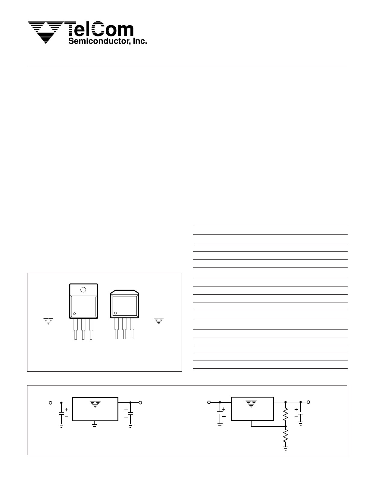
PIN CONFIGURATIONS
TO-220-3 DDPAK-3
3
3
TCL1584CAB
TCL1585CAB
TCL1587CAB
NOTE: For TO-220 ΘJA = 53°C/W. For DDPAK-3 ΘJA = 76°C/W. ΘJA for both packages
are specified without external heat sinks. See Applications Section for details.
12
OUT
V
ADJ/GND
IN
V
12
OUT
V
ADJ/GND
IN
V
TCL1584CEB
TCL1585CEB
TCL1587CEB
The TCL1584/1585/1587 are low dropout, positive linear voltage regulators. They have a maximum current
output specification of 7A, 5A, 4.6A and 3A respectively.
All three devices are supplied in fixed and adjustable output
voltage versions.
Good transient load response combined with low dropout voltage makes these devices ideal for the latest low
voltage microprocessor power supplies. Additionally, shortcircuit, thermal and safe operating area (SOA) protection is
provided internally to ensure reliable operation.
The TCL1587, TCL1585 and TCL1584 are available in
a 3-pin TO-220 tabbed power package and in a 3-pin surface
mount DDPAK-3 package.
ORDERING INFORMATION
Part Number Package Temp. Range
TCL1584-3.3CAB TO-220-3 0°C to + 70°C
TCL1584-3.3CEB DDPAK-3 0°C to + 70°C
TCL1584-ADJCAB TO-220-3 0°C to + 70°C
TCL1584-ADJCEB DDPAK-3 0°C to + 70°C
TCL1585-1.5CAB TO-220-3 0°C to + 70°C
TCL1585-1.5CEB DDPAK-3 0°C to + 70°C
TCL1585-3.3CAB TO-220-3 0°C to + 70°C
TCL1585-3.3CEB DDPAK-3 0°C to + 70°C
TCL1585-ADJCAB TO-220-3 0°C to + 70°C
TCL1585-ADJCEB DDPAK-3 0°C to + 70°C
TCL1587-1.5CAB TO-220-3 0°C to + 70°C
TCL1587-1.5CEB DDPAK-3 0°C to + 70°C
TCL1587-3.3CAB TO-220-3 0°C to + 70°C
TCL1587-3.3CEB DDPAK-3 0°C to + 70°C
TCL1587-ADJCAB TO-220-3 0°C to + 70°C
TCL1587-ADJCEB DDPAK-3 0°C to + 70°C
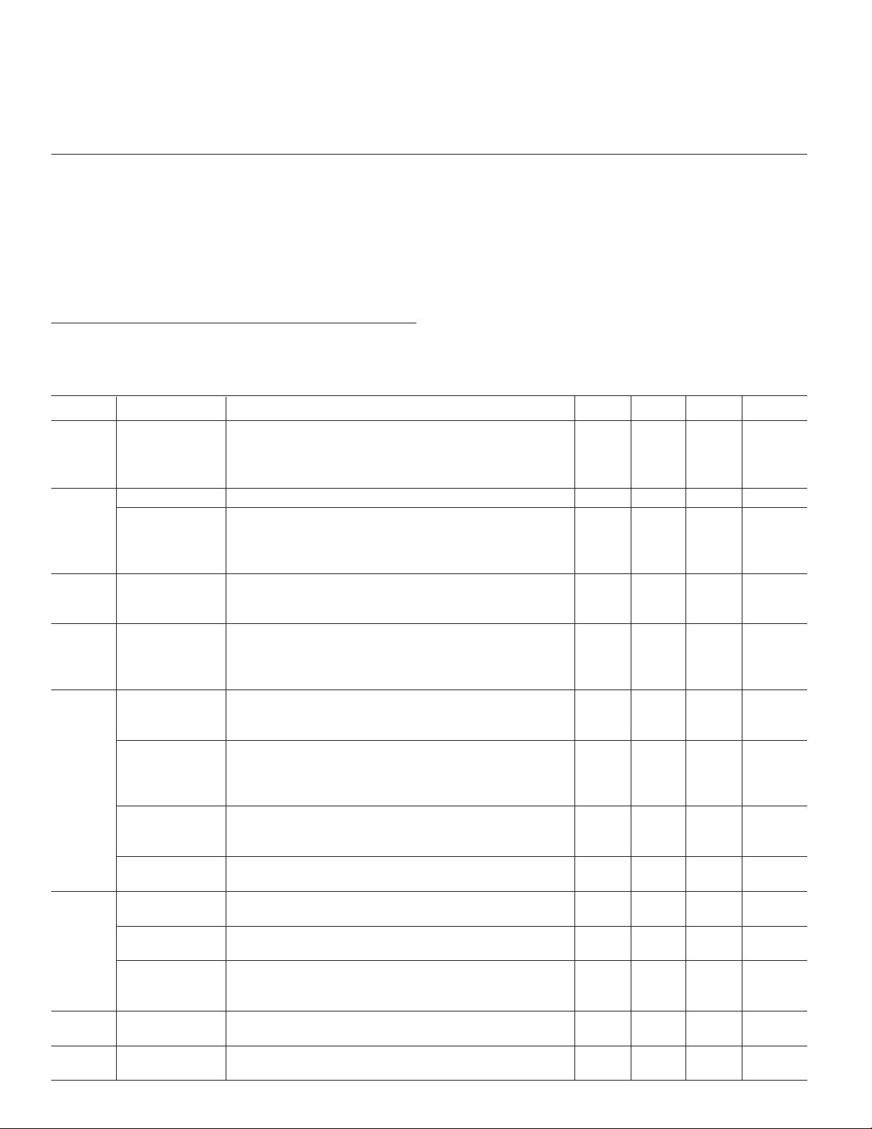
TYPICAL OPERATING CIRCUIT
Fixed Output Voltage Version
GND
V
OUT
section.
= 5V
V
IN
C1 = 10µF
*NOTE: C2 is required to ensure output stability. Minimum 22µF (TCL1584) or 10µF (TCL1585/7),
*All Trademarks and Trade Names are the property of their respective owners.
TCL1584/1585/1587-04 6/6/97
TCL1584/1585/1587-04 6/6/97 TelCom Semiconductor reserves the right to make changes in the circuitry and specifications of its devices.
low ESR tantalum type. Larger values may be required for high output current transient
regulation. See
V
IN
TCL158x-3.3
Applications
V
OUT
C2*
(Tantalum)
= 3.3V
V
IN
1
= 5V
C1 = 10µF
Adjustable Output Voltage Version
V
IN
TCL158x
ADJ
V
OUT
R1
R2
V
OUT
(1+ R1/R2)V
C2*
(Tantalum)
=
REF
PRELIMINARY INFORMATION
TCL1584
TCL1585
TCL1587
7A / 5A / 4.6A / 3A, FAST RESPONSE,
LOW DROPOUT POSITIVE LINEAR
VOLTAGE REGULATORS
ABSOLUTE MAXIMUM RATINGS*
Input Voltage (VIN to GND) ...........................................7V
Operating Junction Temperature Range
*This is a stress rating only, and functional operation of the device at these
or any other conditions beyond those indicated in the operation section of
the specifications is not implied. Exposure to absolute maximum ratings
conditions for extended periods of time may affect device reliability.
Control Circuitry...................................0°C to +125°C
Output Transistor.................................0°C to +150°C
Power Dissipation ..................... See
Applications
Section
Storage Temperature (unbiased) .......... – 65°C to +150°C
Lead Temperature (Soldering, 10 sec) .................+300°C
ELECTRICAL CHARACTERISTICS: T
= Operating Temperature Range, 4.75V ≤ VIN ≤ 5.25V, unless
A
otherwise specified.
Parameter
Reference TCL1584 1.5V ≤ (V
Voltage TCL1585 1.5V ≤ (V
Output TCL1587-1.5 4.75V ≤ V
Voltage TCL1584-3.3 4.75V ≤ V
Line TCL1584/5/7 2.75V ≤ V
Regulation TCL1587-1.5 4.75V ≤ V
(Notes 1, 2)
Load TCL1584/5/7 (V
Regulation TCL1587-1.5 V
(Notes 1, TCL1584/5/7-3.3 V
2, 3) Over Operating Temperature Range — 0.05 0.5
Dropout TCL1585/7 ∆V
Voltage TCL1587-1.5 ∆V
Current TCL1584 (V
Limit TCL1584-3.3 (V
(Note 3)
Temperature
Coefficient
ADJ Pin TCL1584/5/7 — 55 120 µA
Current
TCL1584/1585/1587-04 6/6/97
Device Test Conditions Min Typ Max Unit
– V
1.5V ≤ (V
TCL1587 1.5V ≤ (V
TCL1585-3.3 4.75V ≤ V
4.75V ≤ V
TCL1587-3.3 4.75V ≤ V
TCL1584/5/7-3.3 4.75V ≤ V
– V
IN
= 5V, TJ = 25°C, 0mA ≤ I
IN
= 5V, TJ = 25°C, 0mA ≤ I
IN
= 1%, I
REF
= 1%, I
∆V
∆V
OUT
OUT
REF
REF
OUT
OUT
REF
OUT
REF
OUT
IN
IN
IN
IN
IN
IN
IN
= 1%, I
= 1%, I
= 1%, I
= 1%, I
= 1%, I
= 1%, I
= 1%, I
= 1%, I
= 1%, I
– V
– V
– V
– V
– V
– V
– V
TCL1585/7-3.3 ∆V
TCL1585 ∆V
TCL1585-3.3 ∆V
TCL1584 ∆V
TCL1584-3.3 ∆V
TCL1584 ∆V
TCL1584-3.3 ∆V
TCL1585 (V
TCL1585-3.3 (V
TCL1587 (V
TCL1587-1.5 (V
TCL1587-3.3 (V
TBD TBD
IN
IN
IN
IN
IN
IN
IN
IN
IN
IN
IN
IN
OUT
) ≤ 3V, 10mA ≤ I
OUT
– V
) ≤ 5.75V, 10mA ≤ I
OUT
– V
) ≤ 5.75V, 10mA ≤ I
OUT
– V
) ≤ 5.75V, 10mA ≤ I
OUT
≤ 7V, 0mA ≤ I
≤ 6.3V, 0mA ≤ I
≤ 7V, 0mA ≤ I
≤ 7V, 0mA ≤ I
≤ 7V, 0mA ≤ I
≤ 7V, I
OUT
≤ 7V, I
OUT
≤ 7V, I
OUT
≤ 3A
OUT
OUT
≤ 4.6A, TJ ≥ 25°C
OUT
≤ 4A, TJ < 25°C
OUT
≤ 3A
OUT
= 10mA — 0.005 0.2 %
= 0mA
= 0mA
) = 3V, TJ = 25°C, 10mA ≤ I
OUT
OUT
= 3A — 1.15 1.30 V
OUT
= 3A
OUT
= 3A
OUT
= 4.6A, TJ ≥ 25°C — 1.20 1.40 V
OUT
= 4A, TJ < 25°C
OUT
= 4.6A, TJ ≥ 25°C
OUT
= 4A, TJ < 25°C
OUT
= 6A
OUT
= 6A:TJ ≥ 25°C — 1.20 1.30 V
OUT
TJ < 25°C — 1.30 1.35
= 7A — 1.25 1.40 V
OUT
= 7A
OUT
) = 3V 7.10 8.25 — A |
OUT
) = 3V
OUT
) = 5.5V: TJ < 25°C 4.10 5.25 — A
OUT
) = 5.5V: TJ ≥ 25°C 4.60 5.25
OUT
) = 5.5V 3.10 3.75 — A
OUT
) = 5.5V
OUT
) = 5.5V
OUT
≤ 7A 1.225 1.25 1.275 V
OUT
≤ 4.6A, TJ ≥ 25°C
OUT
≤ 4A, TJ < 25°C
OUT
≤ 3A
OUT
≤ 7A 3.235 3.30 3.365 V
≤ I
FULL LOAD
≤ I
FULL LOAD
2
OUT
≤ I
FULL LOAD
— 0.05 0.3 %
7A / 5A / 4.6A / 3A, FAST RESPONSE,
LOW DROPOUT POSITIVE LINEAR
VOLTAGE REGULATORS
PRELIMINARY INFORMATION
TCL1584
TCL1585
TCL1587
ELECTRICAL CHARACTERISTICS: (Cont.) T
= Operating Temperature Range, 4.75V ≤ VIN ≤ 5.25V,
A
unless otherwise specified.
Parameter
ADJ Pin TCL1584 1.5V ≤ (V
Current TCL1585/7 1.5V ≤ (V
Change
(Note 3)
Minimum TCL1584/5/7 1.5V ≤ (V
Load
Current
Quiescent TCL1587-1.5 VIN = 5V — 8 13 mA
Current TCL1584/5/7-3.3 VIN = 5V
Ripple TCL1584 f = 120Hz, C
Rejection TCL1584-3.3 f = 120Hz, C
Thermal TCL1584/5/7 TA = 25°C, 30msec Pulse — 0.004 0.02 %/W
Regulation TCL1587-1.5 T
Temperature
Stability
Long Term TA = 125°C, 1000Hrs. — 0.03 1.0 %
Stability
RMS TA = 25°C, 10Hz ≤ f ≤ 10kHz — 0.003 — %
Output
Noise (%
of V
OUT
Thermal TCL1584 “A” pkg. (TO-220): Control Circuitry/Power Transistor — — 0.65/2.7 °C/W
Resistance TCL1585 “A” pkg. (TO-220): Control Circuitry/Power Transistor — — 0.7/3.0 °C/W
(Junction to
Case, ΘJA)
NOTES: 1. See thermal regulation specifications for changes in output voltage due to heating effects. Load and line regulation are measured at a constant
Device Test Conditions Min Typ Max Unit
– V
IN
IN
IN –VOUT
TCL1585
f = 120Hz, C
f = 120Hz, C
TCL1585-3.3 f = 120Hz, C
f = 120Hz, C
TCL1587 f = 120Hz, C
TCL1587-1.5 f = 120Hz, C
TCL1587-3.3 f = 120Hz, C
= 25°C, 30msec Pulse
A
) ≤ 3V, 10mA ≤ I
OUT
– V
) ≤ 5.75V, 10mA ≤ I
OUT
) ≤ 5.75V — 2 10 mA
= 25µF Tant. (V
OUT
= 25µF Tant., V
OUT
= 25µF Tant., (V
OUT
= 25µF Tant., (V
OUT
= 25µF Tant.,V
OUT
= 25µF Tant.,V
OUT
= 25µF Tant., (V
OUT
= 25µF Tant., V
OUT
= 25µF Tant., V
OUT
IN
IN
TCL1584/5/7-3.3 TA = 25°C, 30msec Pulse
VIN = 5V, I
= 0.5A — 0.5 — %
OUT
)
TCL1585 “E” pkg. (TO-263): Control Circuitry/Power Transistor — — 0.7/3.0 °C/W
TCL1587 “A” pkg. (TO-220): Control Circuitry/Power Transistor — — 0.7/3.0 °C/W
TCL1587 “E” pkg. (TO-263): Control Circuitry/Power Transistor — — 0.7/3.0 °C/W
junction temperature by low duty cycle pulse testing.
2. Load and line regulation are guaranteed up to the maximum power dissipation (25W for the TCL1584 in “A” pkg., 26.5W for the TCL1585 in
“A” pkg., 18W for the TCL1587 in “A” pkg.). Power dissipation is determined by input/output voltage differential and output current. Guaranteed
maximum output current/power will not be available over full input/output voltage range.
3. I
FULL LOAD
TCL1584, decreasing to approximately 3A as V
the TCL1587, I
is defined as the maximum value of output load current as a function of input-to-output voltage. I
FULL LOAD
is 3A. The TCL1585 and 1587 have constant current limit with respect to V
– V
IN
increases from 3V to 7V. For all other fixed voltage TCL1585’s, I
OUT
OUT
– V
IN
= 5.8V, I
IN
– V
OUT
– V
OUT
= 6.3V, I
IN
= 6.3V, I
IN
– V
IN
= 5.0V, I
IN
= 6.3V, I
IN
≤ I
FULL LOAD
≤ I
OUT
) = 2.5V, I
OUT
OUT =
) = 3V, I
) = 3V, I
OUT
OUT
) = 3V, I
OUT
OUT
OUT
FULL LOAD
= 7A 60 72 — dB
OUT
7A
= 4.6A, TJ ≥ 25°C
OUT
= 4A, TJ ≤ 25°C
OUT
= 4.6A, TJ ≥ 25°C
= 4.6A, TJ ≤ 25°C
= 3A
OUT
= 3A
= 3A
— 0.2 5 µA
is a nominal 7A for
FULL LOAD
.
is 4A. For
IN
and V
FULL LOAD
OUT
TCL1584/1585/1587-04 6/6/97
3
PRELIMINARY INFORMATION
TCL1584
TCL1585
TCL1587
Typical Dropout Voltage vs. Output Current
1.5
1.4
1.3
1.2
1.1
1.0
0.9
0.8
0.7
0.6
INPUT/OUTPUT DIFFERENTIAL (V)
0.5
0I
OUTPUT CURRENT (A)
7A / 5A / 4.6A / 3A, FAST RESPONSE,
LOW DROPOUT POSITIVE LINEAR
VOLTAGE REGULATORS
FULL LOAD
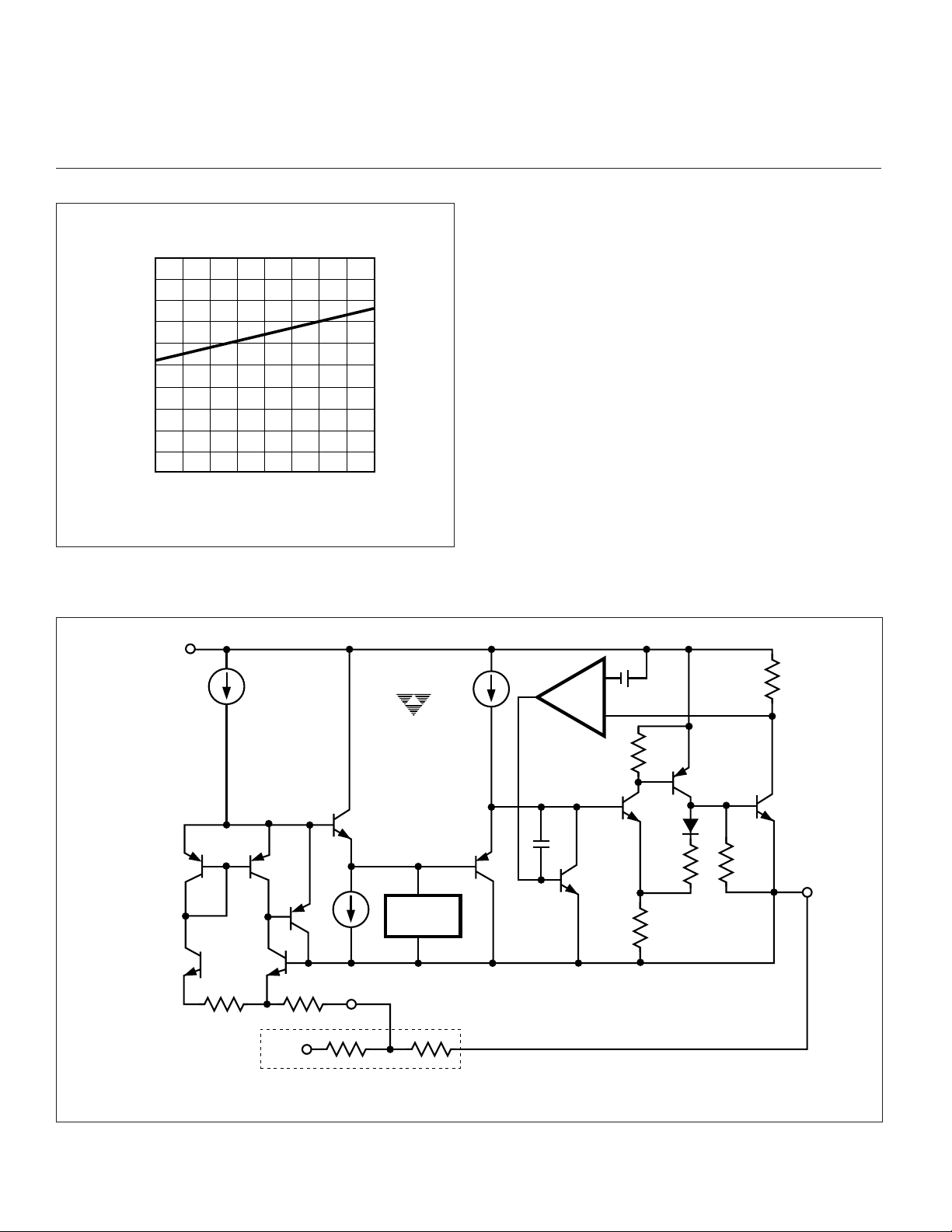
SIMPLIFIED SCHEMATIC
V
IN
GND
ADJ
TCL1584/5/7
THERMAL
LIMIT
+
–
V
OUT
TCL1584/1585/1587-04 6/6/97
FOR FIXED VOLTAGE DEVICE
4

7A / 5A / 4.6A / 3A, FAST RESPONSE,
LOW DROPOUT POSITIVE LINEAR
VOLTAGE REGULATORS
PRELIMINARY INFORMATION
TCL1584
TCL1585
TCL1587
APPLICATIONS
General
The TCL158x family of devices combine high current
output (up to 7A) with low dropout voltage and built-in fault
protection in a traditional three-terminal LDO format. All
three device types are available in fixed output voltage and
adjustable output versions. Fault protection includes shortcircuit current limit, over-temperature limit, and safe-operating-area (SOA) governing.
These devices are pin-compatible upgrades for the
1083/1084/1085 family of LDO’s. However, the TCL158x
family delivers lower dropout voltage, faster load transient
response and improved internal frequency compensation.
Maximum supply voltage rating is 7.0V.
Modern processors cycle load current from near zero to
several amps in a time period measured in tens of nanoseconds. Load step response requirements are worsened by
tighter output voltage tolerances. The TCL1584/85/87 family of regulators meets these stringent requirements without
an obnoxious amount of output capacitance, saving both
board space and cost.
Stability and Transient Response
Like most low dropout voltage regulators, the TCL158x
devices require the use of output capacitors to maintain
stability. Normally a 22µF solid tantalum or a 100µF aluminum electrolytic unit will ensure stability over all operating
conditions. Keep in mind that commercially available capacitors can have significant non-ideal effects such as
capacitance value tolerance, temperature coefficient, ESR,
ESL. The TCL158x devices are optimized for use with low
ESR (<1Ω) capacitors.
On the adjustable voltage versions, bypassing the ADJ
pin will improve ripple rejection and transient response. This
is discussed in the
increases the required output capacitance value. The previously suggested minimum values (22µF and 100µF) take
this into account. If no bypassing is used, lower values of
output capacitance may be used.
Transient regulation is directly related to output capacitance value. For applications which require large load current step changes, it is recommended that large output
capacitors (>100µF) be used. The value of the output
capacitor can be increased without limit and will only improve transient regulation.
In a typical high-performance microprocessor application, the sudden transients can be so fast that the output
decoupling network must handle the sudden current demand until the internal voltage regulator is able to respond.
In this case the non-ideal effects of the output capacitor are
critical in determining the regulator’s response. Output volt-
TCL1584/1585/1587-04 6/6/97
Ripple Rejection
section. This bypassing
age response to step load current change is illustrated in
Figure 1. The capacitor’s ESR and ESL cause immediate
step changes in the output voltage. These are calculated as
follows:
∆V
= ∆I x ESR
ESR
DV
= DI/Dt x ESL
ESL
To reduce the initial voltage droop, one should select
low ESR and ESL capacitors. It should also be noted that the
ESR effect is multiplied by absolute change in load current
while the ESL effect is multiplied by the
rate of change
current. After the initial voltage drop, the capacitor value
dominates the rate of change in voltage. This rate is calculated as follows:
∆V = ∆t x ∆I/C
ESR
EFFECTS
ESL
EFFECTS
SLOPE,
V = ∆I
t C
POINT AT WHICH REGULATOR
TAKES CONTROL
Figure 1. Transient Load Voltage Response
CAPACITANCE
EFFECTS
Typically high quality ceramic and tantalum capacitors
must be used in combination to minimize ESR and maximize
C. This decoupling network must also be placed close to the
microprocessor to reduce ESL (parasitic board trace inductance). If possible, the capacitors should be placed
the microprocessor socket cavity. Of course, robust power
and ground planes will also improve performance by reducing parasitic voltage drops.
The TCL1584 has an adaptive current limiting scheme
where to ensure SOA for the output transistor, the current
limit is reduced for increasing input to output differential. This
means that the TCL1584 exhibits a
characteristic
under certain conditions. This is a common
negative resistance
technique in LDO design to ensure SOA - especially LDO’s
with high maximum input voltage ratings. This negative
resistance can interact with the external capacitance and
inductance and cause oscillations during current limit. This
effect is highly dependent on system parameters and is
difficult to predict. However this oscillation, if it occurs, will
not damage the regulator and can be ignored if the system
5
in load
inside

PRELIMINARY INFORMATION
TCL1584
TCL1585
TCL1587
7A / 5A / 4.6A / 3A, FAST RESPONSE,
LOW DROPOUT POSITIVE LINEAR
VOLTAGE REGULATORS
parameters will allow it. Typically, increasing the output
capacitance helps reduce the oscillation. NOTE: The
TCL1585 and TCL1584 have fixed current limit over the
entire voltage range and are not susceptible to this phenomenon.
Protection Diodes
The TCL158x family of devices do not normally require
any external current limiting circuitry such as protection
diodes, frequently used with older LDO regulators. A diode
is internally present between the output and input which is
capable of handling short-duration surge currents of up to
100A. This capability typically ensures safe operation except for the case where output capacitance is exceedingly
large (>1000µF) and the input is suddenly shorted to ground.
This situation can produce excessive reverse current in the
device - enough to cause damage. An external high current
diode should be used as shown in Figure 2.
The ADJ pin does not normally need protection diodes
either. It can handle ±7V without any performance degradation or device damage. Current at this pin is internally limited
by a series resistor so the bypass capacitors do not present
any danger. Of course, exceeding 7V differential between
any two pins will cause catastrophic junction breakdowns
and possible damage to the device.
D1
1N4002
(OPTIONAL)
V
IN
+
IN
C1
10µF
TCL1584-3.3
GND
OUT
+
C2
22µF
V
OUT
Overload Recovery
The built-in Short Circuit and Safe-Operating-Area (SOA)
protection function of the TCL158x family can cause secondary effects which must be considered for robust system
design. The behavior of the regulator under heavy loads
(short circuit) at start-up is such that the output voltage will
remain low while sourcing maximum current until the load is
removed or reduced. Normally, the output voltage will rise as
the load is reduced and trace a line I-V relationship according to the SOA limit. If the load line intersects this output
curve at two points the output voltage may not recover from
the heavy load/short-circuit condition. This condition is illustrated in Figure 3. The current limit constraint does not allow
any load point above it and the load line is defined absolutely
by the I-V characteristics of the load (a resistor, in this case).
Under these conditions it may be necessary to cycle the
power supply off and then on again. This phenomenon is
common for LDO’s with fold-back current limiting schemes.
NOTE: Overload recovery is
always
guaranteed on the
TCL1585 and TCL1587 because of the constant current
limit characteristic.
Ripple Rejection
A typical ripple rejection curve for the fixed output
voltage devices is shown in Figure 3. It is possible to obtain
improved performance in ripple rejection by using the adjustable output TCL158x with a bypass capacitor (C
shown in Figure 2. This capacitor should be chosen to have
a value such that its impedance at the ripple frequency is
less than R1 (see Figure 2.). Usually this is on the order of
100Ω. Example: If R1 = 100Ω and f
= 120Hz, the
RIPPLE
bypass capacitor should be chosen to be 22µF or greater. If
these conditions are met the ripple rejection will be improved
by a factor of V
/1.25 when compared to the performance
OUT
of the fixed output devices.
ADJ
)
V
IN
C1
10µF
TCL1584/1585/1587-04 6/6/97
IN
+
Figure 2. Protection Diodes and C
D1
1N4002
(OPTIONAL)
TCL1584
ADJ
+
C
ADJ
OUT
R1
R2
+
ADJ
C2
22µF
V
OUT
Current Limit Curve
I
OUT
Load Line
–
V
OUT
(Constant V
V
IN
Figure 3. Overload Recovery
6
Unrecoverable
I-V Point
)
IN
Start Up
Point

7A / 5A / 4.6A / 3A, FAST RESPONSE,
R
L
OUTIN
TCL1584
R
P
PARASITIC
LINE RESISTANCE
*CONNECT R1 TO CASE
CONNECT R2 TO LOAD
ADJ
V
IN
R1*
R2*
LOW DROPOUT POSITIVE LINEAR
VOLTAGE REGULATORS
PRELIMINARY INFORMATION
TCL1584
TCL1585
TCL1587
Output Voltage
The output voltage for the fixed output versions of the
TCL158x is set internally and cannot be adjusted. For the
adjustable output versions, the output voltage is set by two
external resistors: R1 and R2 (see Figure 3). A 1.25V
reference voltage is maintained between the OUTPUT pin
and the ADJ pin. NOTE: the ADJ pin typically will source
55µA. R1 should be chosen to conduct at least the specified
minimum load current of 10mA (i.e. at most 125Ω). Now R2
will determine the total output voltage according to the
equation below:
V
= V
OUT
The contribution due to the I
as I
is only 55µA compared to 10mA for the total current
ADJ
in the adjust circuit.
V
IN
+
C1
10µF
(1+ R2/R1) + R2(I
REF
TCL1584
ADJ
I
ADJ
55µA
)
ADJ
term is relatively small
ADJ
OUTIN
V
REF
R1
V
C2
22µF
OUT
R
P
PARASITIC
V
IN
TCL1584-3.3
GND
Figure 5. Connection for Best Load Regulation
LINE RESISTANCE
OUTIN
R
L
In both cases, because the effect of parasitic trace
resistance (RP) cannot be completely eliminated, it is important to keep the positive output lead as short as possible.
Otherwise, at high output currents, the load regulation will
degrade appreciably. Example:
RP = 5mΩ
I
= 3A
OUT
V
= (0.005) x (3) = 15mV
DROP
Load Regulation
Because the TCL158x family are three terminal devices, it is not possible to perform true Kelvin load voltage
sensing. Therefore load regulation is limited somewhat by
parasitic trace resistance. The load regulation specifications
are measured
degradation in load regulation performance the following
guidelines should be used.
For fixed voltage devices, the GND pin should be
connected directly to the negative side of the load instead of
to a common ground bus. This provides Kelvin sensing at
the negative side while the positive side is still limited by R
(See Figure 5).
For adjustable output devices, the bottom of R2 connects to the negative side of the load. For the positive side,
best regulation is obtained when the top of R1 is connected
directly to the TCL158x and not to the load (See Figure 6).
If R1 connects to the load the effective resistance between
the output and the load is:
RP x (1 + R2/R1)
TCL1584/1585/1587-04 6/6/97
V
= V
OUT
Figure 4. Adjustable Voltage Regulator
directly
REF
1+ R2 ) + I
(
R1
ADJ
(R2)
at the TCL158x package. To minimize
R2
Figure 6. Connection for Best Load Regulation
P
Thermal Considerations
The TCL158x family includes built-in thermal overload
protection. However, maximum operating junction temperature
devices are capable of dissipating up to 25W or more under
must not be exceeded
for any condition. Since these
some conditions, careful thermal design is required for
reliable, continuous operation. In most cases, external heat
sinking will be required.
7

PRELIMINARY INFORMATION
TCL1584
TCL1585
TCL1587
7A / 5A / 4.6A / 3A, FAST RESPONSE,
LOW DROPOUT POSITIVE LINEAR
VOLTAGE REGULATORS
When generating the overall thermal design, it is important to consider all sources of thermal resistance between
the silicon die and ambient - junction-to-case (ΘJC), case-toheat sink (ΘCH), heat sink-to-ambient (ΘHA). NOTE: there
are two separate ΘJC specifications for the power transistor
and the control circuitry. Both junction temperatures must be
calculated and kept under each respective maximum limit to
ensure proper operation. This ΘJC is for the physical path
between the die and the bottom metal portion of the case
(both TO-220 and DDPAK-3. Heat flow will be greatest
through this path. It is important that good thermal coupling
is made between the case and heat sink. If electrical
isolation from the heat sink is not required, it is recommended that thermally conductive compound be used.
Otherwise, use a thermally conductive dielectric spacer.
The following is a thermal design example:
Using a TCL1585-3.3 in a TO-220 package:
Assumptions:
TA = +70°C
VIN = 5.25V (5V + 5%)
V
= 3.30V
OUT
I
= 4.6A
OUT
NOTE: Without heat sinking, the thermal resistance for the
TO-220 and DDPAK-3 packages are 53°C/W and
76°C/W respectively.
ΘHA = 3.5°C/W (heat sink-to-ambient)
ΘCH = 1.5°C/W (case-to-heat sink)
ΘJC = 3°C/W (power transistor)
ΘJC = 0.7°C/W (control circuitry)
Power dissipation:
PD = (VIN – V
Junction Temperatures:
TJ = TA + PD(ΘHA + ΘCH + ΘJC)
Control Circuitry:
TJ = 70 + 8.97(3.5 + 1.5 + 0.7) = 121.1°C
Power Transistor:
TJ = 70 + 8.97(3.5 + 1.5 + 3) = 141.8°C
These values for TJ fall within the maximum allowed
junction temperature for each die section indicating adequate heat sinking with some margin.
OUT
)(I
) = (5.25 – 3.3)(4.6) = 8.97W
OUT
TCL1584/1585/1587-04 6/6/97
8

7A / 5A / 4.6A / 3A, FAST RESPONSE,
LOW DROPOUT POSITIVE LINEAR
VOLTAGE REGULATORS
TYPICAL APPLICATIONS
Typical Intel™* 486Dx4 Microprocessor Application
PRELIMINARY INFORMATION
TCL1584
TCL1585
TCL1587
V
≥ 4.75V
IN
4.75V TO 5.25V
C1 TO C3
AVX TPS
3 EACH
220µF
10V
V
IN
C1
10µF
10V
THERMALLOY
V
IN
330µF
AVX X7R 0805
PLACE AT MICROPROCESSOR SOCKET V
V
TCL1587-3.3
GND
OUT
C2
22µF
10V
C3 TO C6
47µF
10V
ESR OF THE 47µF IS < 0.1Ω
Intel™* 90MHz Pentium™* Power Supply
7020B-MT
TCL1585
ADJ
C4
16V
V
OUT
R1
110Ω
0.1%
R2
187Ω
0.1%
AVX Corp. (803) 448-9411
Sanyo Video Components (USA) Corp. (619) 661-6322
Thermalloy Inc. (214) 243-4321
DO NOT SUBSTITUTE COMPONENTS
PLACE IN MICROPROCESSOR
SOCKET CAVITY
C5 TO C10
100µF
10V
AVX TPS
6 EACH
C7 TO C15
0.1µF
C11 TO C20
1µF
16V
AVX Y5V 0805
10 EACH
CC
3.30V
C16 TO C24
0.01µF
3.38V
4.6A
PINS
3A
Transient Response for 3.8A Load Current Step*
V
OUT
50mV/DIV
I
OUT
2A/DIV
100µsec/DIV
*TRANSIENT RESPONSE MEASURED WITH AN
INTEL POWER VALIDATOR™. V
AT THE POWER VALIDATOR.
All Trademarks and Trade Names are the property of their respective owners.
TCL1584/1585/1587-04 6/6/97
IS MEASURED
OUT
9

PRELIMINARY INFORMATION
TCL1584
TCL1585
TCL1587
TYPICAL APPLICATIONS (Cont.)
Typical Intel™* Pentium™* Pro GTL+ Bus Terminator Application Using TCL1587-1.5
V
= 5V or 3.3V
IN
C1 = 10µF
V
IN
TCL1587-1.5
GND
7A / 5A / 4.6A / 3A, FAST RESPONSE,
LOW DROPOUT POSITIVE LINEAR
VOLTAGE REGULATORS
V
= 1.5V @ 3A
OUT
V
OUT
C2 = 10µF
(Tantalum)
C3 =1µF x 5
(Ceramic)
R
TERM
= 100Ω x 71
Lines
R
REF
V
= 1.5V @ 3A
OUT
GND
V
OUT
C2 = 10µF
(Tantalum)
loading does not appreciably degrade V
REF
V
= 5V or 3.3V
IN
C1 = 10µF
NOTES: 1. It is recommended that the GTL+ bus be terminated at each end by a separate regulator to avoid power distribution losses.
*All Trademarks and Trade Names are the property of their respective owners.
2. The GTL+ bus transmission line symbol will consist of all the components (chip set IC's) on the GTL+ bus.
3. R
and 2R
REF
Values <100 ohms should suffice for most applications.
4. R
TERM
application information.
V
IN
TCL1587-1.5
should be chosen such that V
REF
will be determined by individual bus physical/electrical parameters. See CPU manufacturer documentation for
GTL+ Bus (Z
C3 = 1µF x 5
(Ceramic)
)
O
R
TERM
= 100Ω x 71
Lines
regulation.
REF
2R
REF
V
= 1.0V
REF
TCL1584/1585/1587-04 6/6/97
10

7A / 5A / 4.6A / 3A, FAST RESPONSE,
LOW DROPOUT POSITIVE LINEAR
VOLTAGE REGULATORS
TYPICAL CHARACTERISTICS
PRELIMINARY INFORMATION
TCL1584
TCL1585
TCL1587
TCL1584 Dropout Voltage vs.
Output Current
1.5
1.4
1.3
1.2
1.1
1.0
0.9
0.8
DROPOUT VOLTAGE (V)
0.7
0.6
INDICATES GUARANTEED TEST POINT
0.5
021
T = 25°C
4
3675
OUTPUT CURRENT (A)
TCL1585 Dropout Voltage vs.
Output Current
1.5
1.4
1.3
1.2
1.1
1.0
0.9
0.8
DROPOUT VOLTAGE (V)
0.7
0.6
0.5
01
T = 25°C
INDICATES GUARANTEED TEST POINT
23 54
OUTPUT CURRENT (A)
T = – 5°C
T = 125°C
T = – 5°C
T = 125°C
TCL1584 Short Circuit Current
vs. Input/Output Differential
10
8
6
4
2
SHORT-CIRCUIT CURRENT (A)
0
02143675
INPUT/OUTPUT DIFFERENTIAL (V)
T = 125°C
T = 25°C
T = – 5°C
MINIMUM
TCL1585 Short-Circuit Current
vs. Temperature
6.0
5.5
5.0
4.5
SHORT-CIRCUIT CURRENT (A)
4.0
–75 –50 –25 0 50 75 100 125 150 17525
TEMPERATURE (°C)
TCL1584 Load Regulation
vs. Temperature
0.10
0.05
–0.05
–0.10
–0.15
OUTPUT VOLTAGE DEVIATION (%)
–0.20
∆I = 7A
0
–75 –50 –25 0 50 75100
TEMPERATURE (°C)
TCL1585 Load Regulation
vs. Temperature
0.10
∆I = 4.6A
0.05
0
–0.05
–0.10
–0.15
–0.20
OUTPUT VOLTAGE DEVIATION (%)
–75 –50 –25 0 50 75 100 125150 17525
TEMPERATURE (°C)
125
150 17525
TCL1587 Dropout Voltage vs.
Output Current
1.5
1.4
1.3
1.2
1.1
1.0
0.9
0.8
0.7
DROPOUT VOLTAGE (V)
0.6
0.5
TCL1584/1585/1587-04 6/6/97
T = 25°C
T = 125°C
INDICATES GUARANTEED TEST POINT
0
1.0 1.5
0.5
OUTPUT CURRENT (A)
T = – 5°C
2.0
2.5
TCL1587 Short-Circuit Current
vs. Temperature
5.0
4.5
4.0
3.5
SHORT-CIRCUIT CURRENT (A)
3.0
3.0
–75 –50 –25 0 50 75
25
TEMPERATURE (°C)
100 125150 175
11
TCL1587 Load Regulation
vs. Temperature
0.10
0.05
–0.05
–0.10
–0.15
OUTPUT VOLTAGE DEVIATION (%)
–0.20
∆I = 3A
0
–75 –50 –25 0 50 75100 125 150 17525
TEMPERATURE (°C)

PRELIMINARY INFORMATION
TCL1584
TCL1585
TCL1587
TYPICAL CHARACTERISTICS (Cont.)
7A / 5A / 4.6A / 3A, FAST RESPONSE,
LOW DROPOUT POSITIVE LINEAR
VOLTAGE REGULATORS
TCL1584/5/7 Reference Voltage
vs. Temperature
1.275
1.270
1.265
1.260
1.255
1.250
1.245
1.240
1.235
REFERENCE VOLTAGE (V)
1.230
1.255
–75 –50 –25 0 50 75 100 125 150 17525
TEMPERATURE (°C)
TCL1584/5/7 Minimum Load Current
vs. Temperature
5
4
3
2
1
MINIMUM LOAD CURRENT (mA)
0
–75 –50 –25 0 50 75100 125 150 17525
TEMPERATURE (°C)
Output Voltage vs Temperature
Using Adjustable TCL1584/5/7
3.70
V
SET WITH 1% RESISTORS
OUT
3.65
3.60
3.55
3.50
3.45
3.40
3.35
3.30
OUTPUT VOLTAGE (V)
3.25
3.20
–75 –50 –25 0 50 75 100 125 150 17525
TEMPERATURE (°C)
V
V
V
OUT
OUT
OUT
V
OUT
= 3.6V
= 3.45V
= 3.38V
= 3.3V
TCL1584/5/7 Adjust Pin Current
vs. Temperature
100
90
80
70
60
50
40
30
20
ADJUST PIN CURRENT (µA)
10
0
–75 –50 –25 0 50 75 100 125 150 17525
TEMPERATURE (°C)
TCL1584/5/7-3.3 Output Voltage
vs.Temperature
3.70
3.65
3.60
3.55
3.50
3.45
3.40
3.35
3.30
OUTPUT VOLTAGE (V)
3.25
3.20
–75 –50 –25 0 50 75100 125 150 17525
V
= 3.3V
OUT
TEMPERATURE (°C)
TCL1584/5/7-3.xx Quiescent
Current vs. Temperature
13
12
11
10
9
8
7
6
5
QUIESCENT CURRENT (mA)
4
3
–75 –50 –25 0 50 75 100 125 150 17525
TEMPERATURE (°C)
TCL1584/5/7 Ripple Rejection
vs. Frequency
90
80
70
60
50
40
30
TCL1584: (VIN – V
TCL1584/87 (V
20
RIPPLE REJECTION (dB)
TCL1584/1585/1587-04 6/6/97
10
0
10
0.5V ≤ V
I
= I
OUT
FULL LOAD
100 1k
RIPPLE
FREQUENCY (Hz)
– V
IN
≤ 2V
OUT
) ≤ 2.5V
OUT
) ≤ 3V
10k
100k
TCL1585/7 Maximum Power
Dissipation*
30
TCL1585
25
TCL1587
20
15
POWER (W)
10
5
0
50 60 70 80 100 110 120 130 140 15090
CASE TEMPERATURE (°C)
*AS LIMITED BY MAXIMUM JUNCTION
TEMPERATURE
12
TCL1584 Maximum Power
Dissipation*
30
TCL1584
25
20
15
POWER (W)
10
5
0
506070 80 100
CASE TEMPERATURE (°C)
*AS LIMITED BY MAXIMUM JUNCTION
TEMPERATURE
110
120 130 140 15090

7A / 5A / 4.6A / 3A, FAST RESPONSE,
LOW DROPOUT POSITIVE LINEAR
VOLTAGE REGULATORS
PACKAGE DIMENSIONS
PRELIMINARY INFORMATION
TCL1584
TCL1585
TCL1587
DDPAK-3
.067 (1.70)
.045 (1.14)
.370 (9.40)
.329 (8.38)
.605 (15.37)
.549 (13.95)
.113 (2.87)
.103 (2.62)
.258 (6.55)
.230 (5.84)
.410 (10.41)
.385 (9.78)
.100 (2.54) TYP.
.410 (10.41)
.390 (9.91)
.051 (1.30)
.049 (1.24)
.037 (0.94)
.026 (0.66)
TO-220-3
.156 (3.96)
.146 (3.71)
DIA.
3° - 7°
(5x)
0.26 (0.66)
0.14 (0.36)
.055 (1.40)
.045 (1.14)
.594 (15.09)
.569 (14.45)
.183 (4.65)
.170 (4.32)
0° - 8°
.185 (4.70)
.165 (4.19)
.055 (1.40)
.045 (1.14)
.010 (0.25)
.000 (0.00)
.110 (2.79)
.068 (1.72)
3° - 7.5°
5 PLCS.
.560 (14.22)
.518 (13.16)
Sales Offices
TelCom Semiconductor
1300 Terra Bella Avenue
P.O. Box 7267
Mountain View, CA 94039-7267
TEL: 415-968-9241
FAX: 415-967-1590
E-Mail: liter@c2smtp.telcom-semi.com
TCL1584/1585/1587-04 6/6/97
.205 (5.21)
.195 (4.95)
.244 (6.20)
.234 (5.94)
.055 (1.40)
.045 (1.14)
.037 (0.94)
.027 (0.69)
.105 (2.67)
.095 (2.41)
TelCom Semiconductor
Austin Product Center
9101 Burnet Rd. Suite 214
Austin, TX 78758
TEL: 512-873-7100
FAX: 512-873-8236
13
.0.20 (0.51)
.012 (0.30)
.115 (2.92)
.095 (2.41)
Dimensions: inches (mm)
TelCom Semiconductor H.K. Ltd.
10 Sam Chuk Street, Ground Floor
San Po Kong, Kowloon
Hong Kong
TEL: 852-2324-0122
FAX: 852-2354-9957
Printed in the U.S.A.
 Loading...