

TelCom Semiconductor Inc TCL1117-ADJCEB, TCL1117-ADJCDB, TCL1117-5.00CEB, TCL1117-3.30CEB, TCL1117-5.00CDB Datasheet
...
800mA LOW DROPOUT POSITIVE REGULATORS
PRELIMINARY INFORMATION
ADJUSTABLE AND FIXED 2.85V, 3.30V, 5.00V
800mA LOW DROPOUT POSITIVE REGULATORS
ADJUSTABLE AND FIXED 2.85V, 3.30V, 5.00V
TCL1117
TCL1117
TCL1117-2.85
TCL1117-2.85
TCL1117-3.30
TCL1117-3.30
TCL1117-5.00
TCL1117-5.00
FEATURES
■ Space-saving SOT-223 Package
■ Pin Compatible with Older Adjustable 3 Terminal
Regulators
■
Adjustable or Fixed Voltages of 2.85V, 3.30V or 5.00V
■ High Output Current ..................................... 800mA
■ Low Dropout Voltage ............1.2V at I
■ Guaranteed Dropout Voltage at Multiple Current
Levels
■ Line Regulation (Max) ......................................0.2%
■ Load Regulation (Max) ..................................... 0.4%
= 800mA
OUT
APPLICATIONS
■ Active SCSI Terminators
■ High Efficiency Linear Regulators
■ Post Regulators for Switching Supplies
■ Battery Chargers
■ 5V - 3.3V Linear Regulators
ORDERING INFORMATION
Part Number* Package Part Marking
TCL1117-ADJCDB SOT-223-3 1117
TCL1117-2.85CDB SOT-223-3 11172
TCL1117-3.30CDB SOT-223-3 11173
TCL1117-5.00CDB SOT-223-3 11175
TCL1117-ADJCEB DDPAK-3
TCL1117-2.85CEB DDPAK-3
TCL1117-3.30CEB DDPAK-3
TCL1117-5.00CEB DDPAK-3
*Ambient temperature range is determined by maximum operating
power dissipation and a maximum die temperature of 125°C (see Power
Dissipation and Thermal Design Section).
GENERAL DESCRIPTION
The TCL1117 is a low-dropout positive voltage regulator (LDO) with 800mA output current capability. It is available
in fixed and adjustable output voltage versions, 2.85V (active SCSI terminators), 3.30V and 5.00V. Output/reference
voltage accuracy is guaranteed to ±1.0%. Over-current
protection is integrated onto the chip. Dropout is specified
at 1.2V maximum at full rated output current and less than
1.0V at low loads (<100mA). The SOT-223 package makes
the TCL1117 especially attractive for tight physical layouts.
For stability, a 10µF output capacitor is required. The
TCL1117 is an NPN-based design which has significantly
lower unused quiescent current than similar PNP-based
regulators.
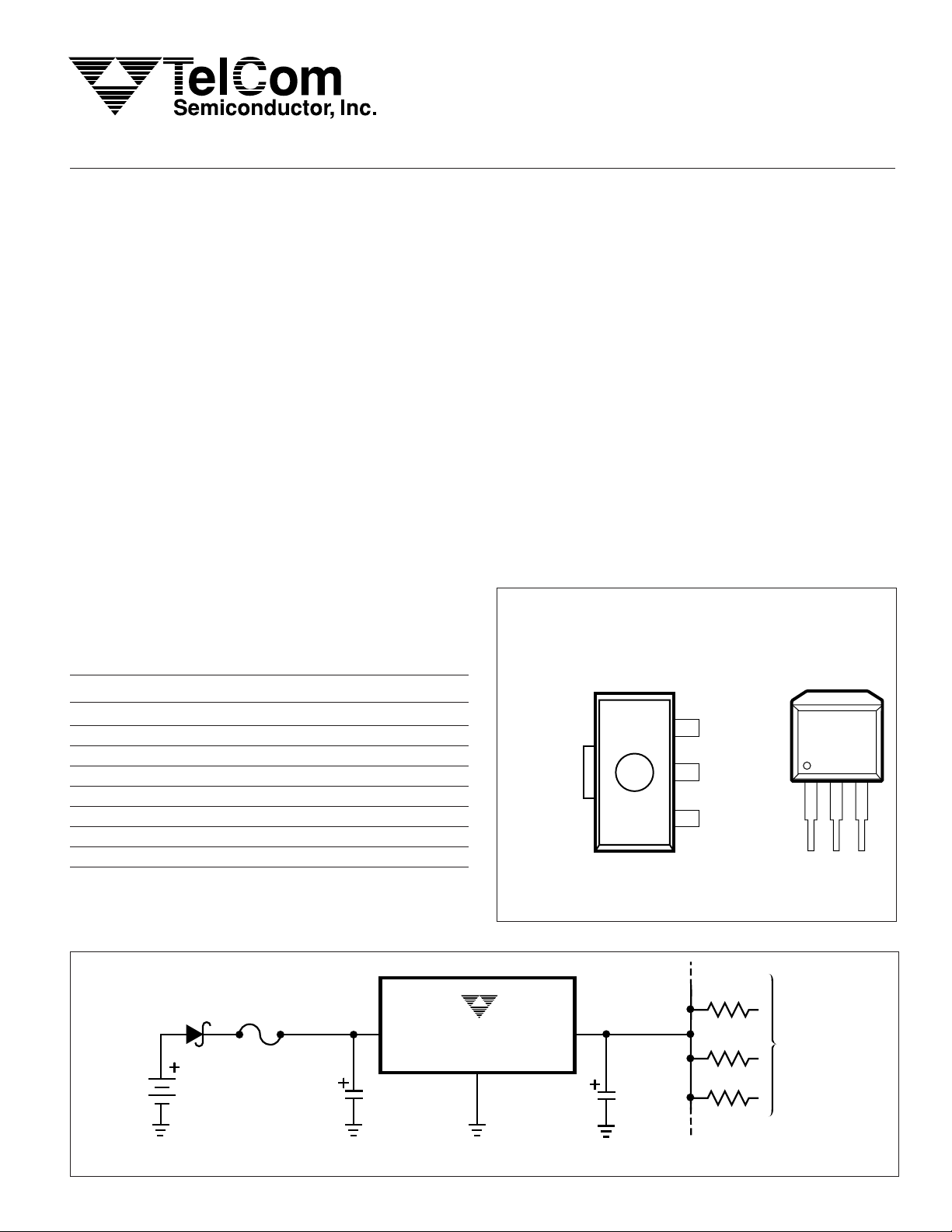
PIN CONFIGURATIONS
TAB IS V
SOT-223
3-Lead Package
FRONT VIEW
OUT
IN
32
OUT
1
ADJ/GND
DDPAK-3
FRONT VIEW
12
3
OUT
ADJ/GND
IN
TYPICAL APPLICATION
4.75V to 5.25V
TCL1117-05 6/5/97
TelCom Semiconductor reserves the right to make changes in the circuitry and specifications of its devices.
TCL1117-5.00
IN
GND
10µF
Active Terminator for SCSI-2 Bus
1
OUT
22µF
110Ω
110Ω
110Ω
18 to 27
LINES
PRELIMINARY INFORMATION
TCL1117
TCL1117-2.85
TCL1117-3.30
TCL1117-5.00
800mA LOW DROPOUT POSITIVE REGULATORS
ADJUSTABLE AND FIXED 2.85V, 3.30V, 5.00V
ABSOLUTE MAXIMUM RATINGS*
Input Voltage
Operating Voltage:
TCL1117, TCL1117-3.30, TCL1117-5.00 ......15V
TCL1117-2.85 ................................................10V
Surge Voltage:
TCL1117, TCL1117-3.30, TCL1117-5.00 ......20V
Storage Temperature ............................– 65°C to +150°C
Lead Temperature (Soldering 10 sec) .................... 300°C
*Stresses beyond those listed under "Absolute Maximum Ratings" may
cause permanent damage to the device. These are stress ratings only, and
functional operation of the device at these or any other conditions beyond
those indicated in the operational sections of the specifications is not
implied. Exposure to absolute maximum rating conditions for extended
periods may affect device reliability.
Operating Junction Temperature ............... 0°C to +125°C
ELECTRICAL CHARACTERISTICS
Symbol Parameter Test Conditions Min Typ Max Unit
Reference TCL1117 I
Voltage 10 ≤ I
Output Voltage TCL1117-2.85 I
TCL1117-3.30 I
TCL1117-5.00 I
Line Regulation TCL1117 I
TCL1117-2.85 I
TCL1117-3.30 I
TCL1117-5.00 I
Load Regulation TCL1117 (V
TCL1117-2.85 V
TCL1117-3.30 V
TCL1117-5.00 V
Dropout Voltage I
Current Limit (V
Minimum Load TCL1117 (V
Current
Quiescent TCL1117-2.85 VIN ≤ 10V (Note 1) — 5 10 mA
Current TCL1117-3.30 V
TCL1117-5.00 VIN ≤ 15V (Note 1) — 5 10
Thermal Regulation TA = 25°C, 30msec Pulse — 0.01 0.1 %W
Ripple Rejection
Adjust Pin Current (Note 1) — 55 120 µA
Adjust Pin Current Change
Temperature Stability — 0.5 — %
Long Term Stability TA = 125°C, 1000 Hrs. — 0.3 — %
RMS Output Noise (% of V
Thermal Resistance (Junction to Case, at Tab) — 15 — °C/W
NOTES: 1. Specifications apply over the full operating temperature range.
2. See thermal regulation specification for changes in output voltage due to heating effects. Load regulation and line regulation are
measured at a constant junction temperature by low duty cycle pulse testing.
3. Dropout voltage is specified over the full output current range of the device. Dropout voltage is defined as the minimum input/output
differential measured at the specified output current. Test points and limits are also shown on the Dropout Voltage curve.
4. Minimum load current is defined as the minimum output current required to maintain regulation.
= 10mA, (VIN – V
OUT
OUT
0 ≤ I
0 ≤ I
OUT
0 ≤ I
OUT
0 ≤ I
OUT
OUT
OUT
OUT
IN
IN
IN
OUT
I
OUT
I
OUT
IN
f
RIPPLE
10mA ≤ I
≤ 800mA, 1.4V ≤ (VIN – V
OUT
= 10mA, VIN = 4.85V, TJ = 25°C 2.820 2.850 2.880 V
≤ 800mA, 4.25V ≤ V
OUT
≤ 500mA, V
OUT
= 10mA, V
≤ 800mA, 4.75V ≤ VIN ≤ 10V (Note 1) 3.230 3.300 3.370
OUT
= 10mA, V
≤ 800mA, 6.50V ≤ V
OUT
= 5.3V, TJ = 25°C 3.265 3.300 3.335 V
IN
= 7V, TJ = 25°C 4.950 5.000 5.050 V
IN
= 10mA, 1.5V ≤ VIN – V
= 0mA, 4.25V ≤ V
= 0mA, 4.75V ≤ V
= 0mA, 6.5V ≤ V
IN – VOUT
) = 3V, 10mA, ≤ I
= 4.25V, 0 ≤ I
= 4.75V, 0 ≤ I
= 6.5V, 0 ≤ I
OUT
OUT
OUT
= 100mA, (Note 1 & 3) — 1.00 1.10 V
= 500mA, (Note 1 & 3) — 1.05 1.15
= 800mA, (Note 1 & 3) — 1.10 1.20
IN – VOUT
IN – VOUT
) = 5V, TJ = 25°C 800 950 1200 mA
) = 15V (Note 1 & 4) — 1.7 5 mA
≤ 15V (Note 1) — 5 10
= 120Hz (VIN – V
≤ 800mA, 1.4V ≤ (V
OUT
10Hz ≤ f ≤ 10kHz — 0.003 — %
OUT),
) = 2V, TJ = 25°C 1.238 1.250 1.262 V
OUT
≤ 10V (Note 1) 2.790 2.850 2.910
IN
= 3.95V (Note 1) 2.790 2.850 2.910
IN
≤ 12V (Note 1) 4.900 5.000 5.100
IN
OUT
≤ 10V (Notes 1 & 2) — 1 6 mV
IN
≤ 15V (Notes 1 & 2) — 1 7
IN
≤ 15V (Notes 1 & 2) — 1 10
IN
OUT
OUT
) ≤ 10V
(Note 1
) 1.225 1.250 1.270
≤ 15V (Notes 1 & 2) — 0.035 0.2 %
≤ 800mA
(Notes 1 & 2)
— 0.1 0.4 %
≤ 800mA (Notes 1 & 2) — 1 10 mV
≤ 800mA (Notes 1 & 2) — 1 12
≤ 800mA (Notes 1 & 2) — 1 15
) = 3V, V
OUT
IN
= 1Vp-p ( Note 1)
RIPPLE
– V
) ≤ 10V (Note 1)
OUT
60 75 — dB
— 0.2 5 µA
TCL1117-05 6/5/97
2
800mA LOW DROPOUT POSITIVE REGULATORS
V
OUT
V
REF
I
ADJ
50µA
R2
V
OUT
= V
REF
(
1+ R2 ) + I
ADJ
R2
R1
R1
OUTIN
TCL1117
ADJ
V
IN
ADJUSTABLE AND FIXED 2.85V, 3.30V, 5.00V
PRELIMINARY INFORMATION
TCL1117
TCL1117-2.85
TCL1117-3.30
TCL1117-5.00
APPLICATIONS
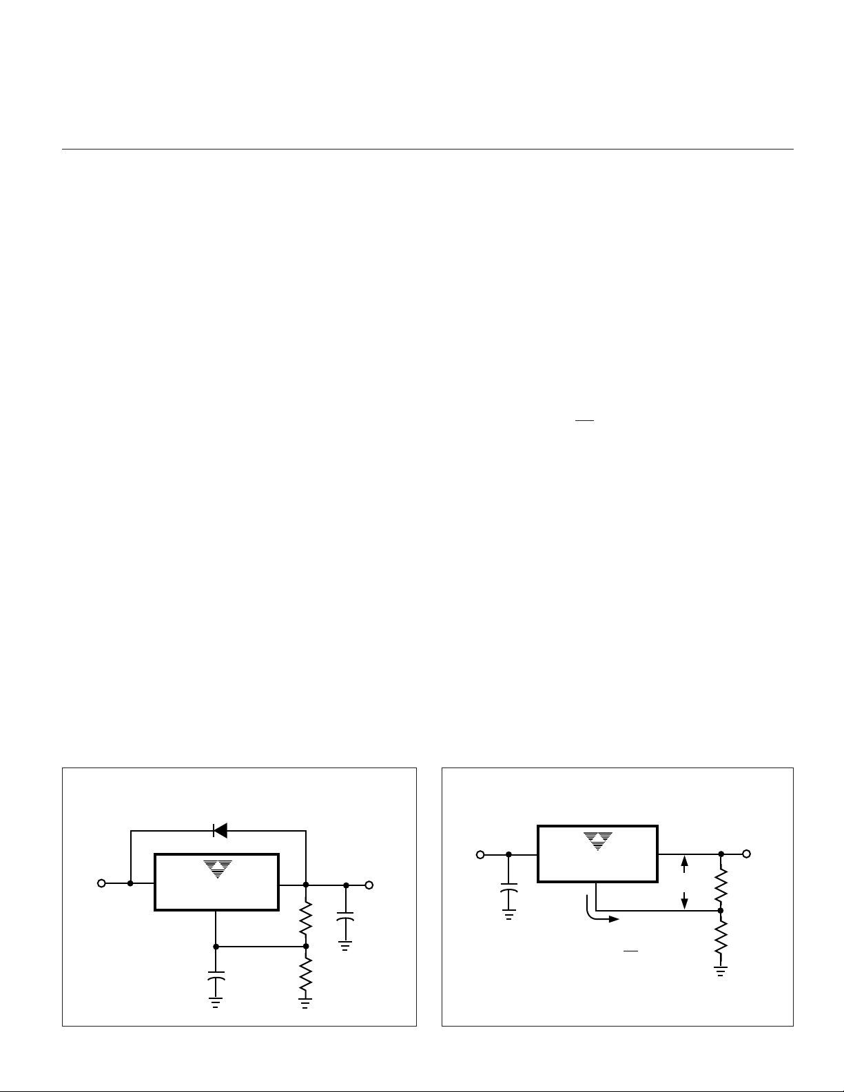
Overload Protection
The TCL1117 is protected against current (short-circuit)
and thermal overload conditions. Thermal protection is
triggered by a chip temperature exceeding 165°C. Current
overload is triggered at approximately 950mA.
Stability and Load Regulation
The TCL1117 requires a capacitor from V
provide compensation feedback to the internal gain stage.
This is to ensure stability at the output terminal. Typically, a
10µF tantalum or 50µF aluminum electrolytic is sufficient.
NOTE: It is important that the ESR for this capacitor does not
exceed 0.5Ω.
The output capacitor does not have a theoretical upper
limit and increasing its value will increase stability.
C
= 100µF or more is typical for high current regulator
OUT
designs. NOTE: See Protection Diodes for limitations. Another benefit of larger output capacitance is improved transient load response (large di/dt in the load).
to GND to
OUT
Protection Diodes
Typically no protection diodes are necessary for the
TCL1117. Unlike older regulators, the ADJ pin is protected
internally from excessive currents. The ADJ pin can be
driven with voltage transients as high as ±25V with respect
to the output without damage to the device.
Likewise, a diode between the input and output is not
typically required. If the input voltage collapses the internal
circuitry can absorb ~20A transient currents (<10µsec)
without damage. This reverse current is much larger than
most power supply designs can generate. However, if the
output capacitor is VERY large (>1000µF), instantaneous
currents can be high enough to damage the chip. In this
case, a high-current, fast-response diode is recommended.
(See Figure 1).
Output Voltage Adjust
Like most LDOs, the TCL1117 regulates the output by
comparing the output voltage, or a multiple thereof, to an
internally generated reference voltage. On the adjustable
version, the V
between V
OUT
is available externally as 1.25V (±1%)
REF
and ADJ (See Figure 2). The voltage divider
formed by R1 and R2 should be set to conduct 10mA
(minimum output load). The output voltage is given by the
following equation:
V
OUT
= V
REF
R1
1+ R2)+ I
(
ADJ
R2
On fixed voltage versions of the TCL1117, the voltage
divider is provided internally.
Load Regulation
The TCL1117 load regulation is limited by the resistance
of the wire connecting it to the load (Rp, Figure 3). For the
adjustable version, the best load regulation is accomplished
when the top of the resistor divider (R1) is connected directly
to the output pin of the TCL1117, NOT to the high side of the
load (Figure 3). When so connected, Rp is not multiplied by
the divider ratio. For the fixed output versions, the top of R1
is internally connected to the output and the ground pin can
be connected to the low side of the load as a negative side
sense if, so desired.
D1
1N4002
(OPTIONAL)
V
IN
TCL1117-05 6/5/97
IN
TCL1117
ADJ
+
Figure 1.
C
ADJ
10µF
OUT
R1
R2
+
C
OUT
150µF
V
OUT
Figure 2. Basic Adjustable Regulator
3
 Loading...