

TelCom Semiconductor Inc TC962MJA, TC962IJA, TC962EPA, TC962CPA, TC962COE Datasheet

HIGH CURRENT CHARGE PUMP DC-TO-DC CONVERTER
EVALUATION
KIT
AVAILABLE
1
TC962
FEATURES
■ Pin Compatible With TC7662/ICL7662/SI7661
■ High Output Current ....................................... 80mA
■ No External Diodes Required
■ Wide Operating Range ............................. 3V to 18V
■ Low Output Impedance .............................28Ω Typ.
■ No Low Voltage Terminal Required
■ Application Zener On Chip
■ OSC Frequency Doubling Pin Option for Smaller
Output Capacitors
PIN CONFIGURATIONS (DIP and SOIC)
8-Pin DIP
ZENER
CATHODE
GND
ZENER
CATHODE
NC
+
C
NC
GND
NC
–
C
NC
FUNCTIONAL BLOCK DIAGRAM
TELCOM SEMICONDUCTOR, INC.
+
C
–
C
16-Pin SOIC Wide
1
2
3
4
5
6
7
8
8-Pin CerDIP
1
2
3
4
•
TC962CPA
TC962EPA
TC962IJA
TC962MJA
TC962COE
FREQ X 2
OSC/C
TIMING
ZENER
CATHODE
8
V
DD
C
7
OSC
6
FREQ x 2
V
5
OUT
16
V
DD
15
NC
14
C
OSC
13
NC
12
FREQ x 2
11
NC
10
V
OUT
9
NC
6
–
7
1
I
I
+
–
COMPARATOR
WITH HYSTERESIS
6.4V
Q
F/F
C
Q
V
REF
GENERAL DESCRIPTION
The TC962 is an advanced version of the industrystandard 7662 high-voltage DC-to-DC converter. Using
improved design techniques and CMOS construction, the
TC962 can source as much as 8mA versus the 7662’s
20mA capability.
As an inverter, the TC962 can put out voltages as high
as 18V and as low as 3V without the need for external
diodes. The output impedance of the device is a low 28Ω
(with the proper capacitors), voltage conversion efficiency
is 99.9%, and power conversion efficiency is 97%.
The low voltage terminal (pin 6) required in some 7662
applications has been eliminated. Grounding this terminal
will double the oscillator frequency from 12kHz to 24kHz.
This will allow the use of smaller capacitors for the same
output current and ripple, in most applications. Only two
external capacitors are required for inverter applications. In
the event an external clock is needed to drive the TC962
(such as paralleling), driving this pin directly will cause the
internal oscillator to sync to the external clock.
ORDERING INFORMATION
Part No. Package Temp. Range
TC962COE 16-Pin SOIC Wide 0°C to +70°C
TC962CPA 8-Pin Plastic DIP 0°C to +70°C
TC962EPA 8-Pin Plastic DIP – 40°C to +85°C
TC962IJA 8-Pin CerDIP – 25°C to +85°C
TC962MJA 8-Pin CerDIP – 55°C to +125°C
TC7660EV Evaluation Kit for Charge Pump Family
8
V
DD
TC962
LEVEL
SHIFT
LEVEL
SHIFT
LEVEL
SHIFT
LEVEL
SHIFT
P SW1
N SW4
N SW2
N SW3
2
+
4
+
CAP
C
P
EXTERNAL
OUT
–
CAP
GND
3
+
C
R
EXT
R
L
5
V
OUT
TC962-8 9/16/96
2
3
4
5
6
7
8
4-37
TC962
HIGH CURRENT CHARGE PUMP
DC-TO-DC CONVERTER
Pin 1, which is used as a test pin on the 7662, is a voltage
reference zener on the TC962. This zener (6.4V at 5 mA) has
a dynamic impedance of 12Ω and is intended for use where
the TC962 is supplying current to external regulator circuitry
and a reference is needed for the regulator circuit. (See
applications section.)
The TC962 is compatible with the LTC1044, SI7661,
and ICL7662. It should be used in designs that require
greater power and/or less input to output voltage drop. It
offers superior performance over the ICL7660S.
ABSOLUTE MAXIMUM RATINGS*
Supply Voltage (VDD to GND) .................................. +18V
Input Voltage Any Pin............... (VDD + 0.3) to (VSS – 0.3)
Current Into Any Pin.................................................10mA
ESD Protection..................................................... ±2000V
Output Short Circuit................. Continuous (at 5.5V Input)
Storage Temperature Range ................– 65°C to +150°C
Lead Temperature (Soldering, 10 sec) .................+300°C
Operating Temperature Range
CPA, COE .............................................0°C to +70°C
IJA ....................................................– 25°C to +85°C
EPA ..................................................– 40°C to +85°C
MJA ................................................– 55°C to +125°C
Package Power Dissipation (TA ≤ 70°C)
SOIC...............................................................760mW
PDIP ...............................................................730mW
CerDIP............................................................800mW
Package Thermal Resistance
CerDIP, R
PDIP, R
*Static-sensitive device. Unused devices must be stored in conductive
material. Protect devices from static discharge and static fields. Stresses
above those listed under Absolute Maximum Ratings may cause permanent damage to the device. These are stress ratings only and functional
operation of the device at these or any other conditions above those
indicated in the operational sections of the specifications is not implied.
Exposure to Absolute Maximum Rating Conditions for extended periods
may affect device reliability.
................................................ 90°C/W
θJ-A
................................................. 140°C/W
θJ-A
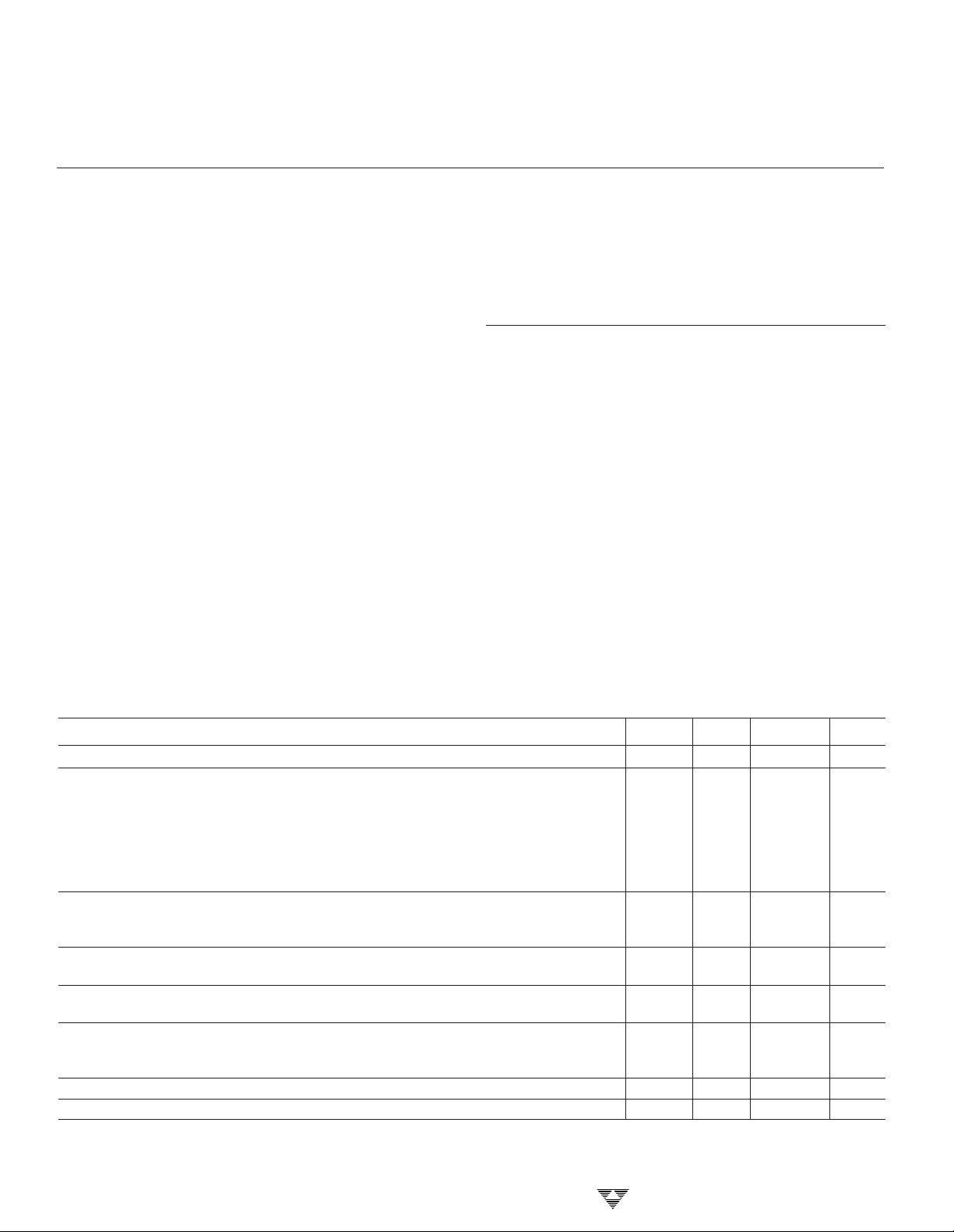
ELECTRICAL CHARACTERISTICS: V
= 15V, TA = +25°C (See Test Circuit), unless otherwise indicated.
DD
Symbol Parameter Test Conditions Min Typ Max Unit
V
I
R
C
P
V
V
Z
DD
S
O
OSC
EFF
DEF
Z
ZT
Supply Voltage 3 18 V
Supply Current RL = ∞
V
= 15V TA = +25°C 510 700 µA
DD
= 5V TA = +25°C 190 µA
V
DD
Output Source IL = 20mA, VDD = 15V — 32 37 Ω
Resistance I
Oscillator Frequency Pin 6 Open — 12 — kHz
Power Efficiency VDD = 15V 93 97 — %
Voltage Efficiency VDD = 15V 99 99.9 — %
Zener Voltage IZ = 5mA 6.0 6.2 6.4 V
Zener Impedance IL = 2.5mA to 7.5mA — 12 Ω
≤ +70°C 560 µA
0 ≤ T
A
–55 ≤ T
0 ≤ T
–55 ≤ TA ≤ +125°C 210 µA
L
IL = 3mA, VDD = 5V — 50 Ω
Pin 6 GND 24 kHz
RL = 2 kΩ
R
Over Temperature Range 96 — %
≤ +125°C 650 µA
A
< +70°C 210 µA
A
= 80mA, VDD = 15V 35 40 Ω
= ∞
L
——— —
4-38
TELCOM SEMICONDUCTOR, INC.
 Loading...