

Datasheet TC9402EJD, TC9402CPD, TC9401EJD, TC9401CPD, TC9400EJD Datasheet (TelCom Semiconductor)
...
TC9400
TC9401
TC9402
VOLTAGE-TO-FREQUENCY/FREQUENCY-TO-VOLTAGE CONVERTERS
1
FEATURES
Voltage-to-Frequency
■ Choice of Guaranteed Linearity:
TC9401.........................................................0.01%
TC9400.........................................................0.05%
TC9402.........................................................0.25%
■ DC to 100 kHz (F/V) or 1Hz to 100kHz (V/F)
■ Low Power Dissipation .......................... 27mW Typ
■ Single/Dual Supply Operation .................................
+ 8V to + 15V or ± 4V to ± 7.5V
■ Gain Temperature Stability ..........± 25 ppm/°C Typ
■ Programmable Scale Factor
Frequency-to-Voltage
■ Operation........................................... DC to 100 kHz
■ Choice of Guaranteed Linearity:
TC9401.........................................................0.02%
TC9400.........................................................0.05%
TC9402.........................................................0.25%
■ Programmable Scale Factor
APPLICATIONS
■ µP Data Acquisition
■ 13-Bit Analog-to-Digital Converters
■ Analog Data Transmission and Recording
■ Phase-Locked Loops
■ Frequency Meters/Tachometer
■ Motor Control
■ FM Demodulation
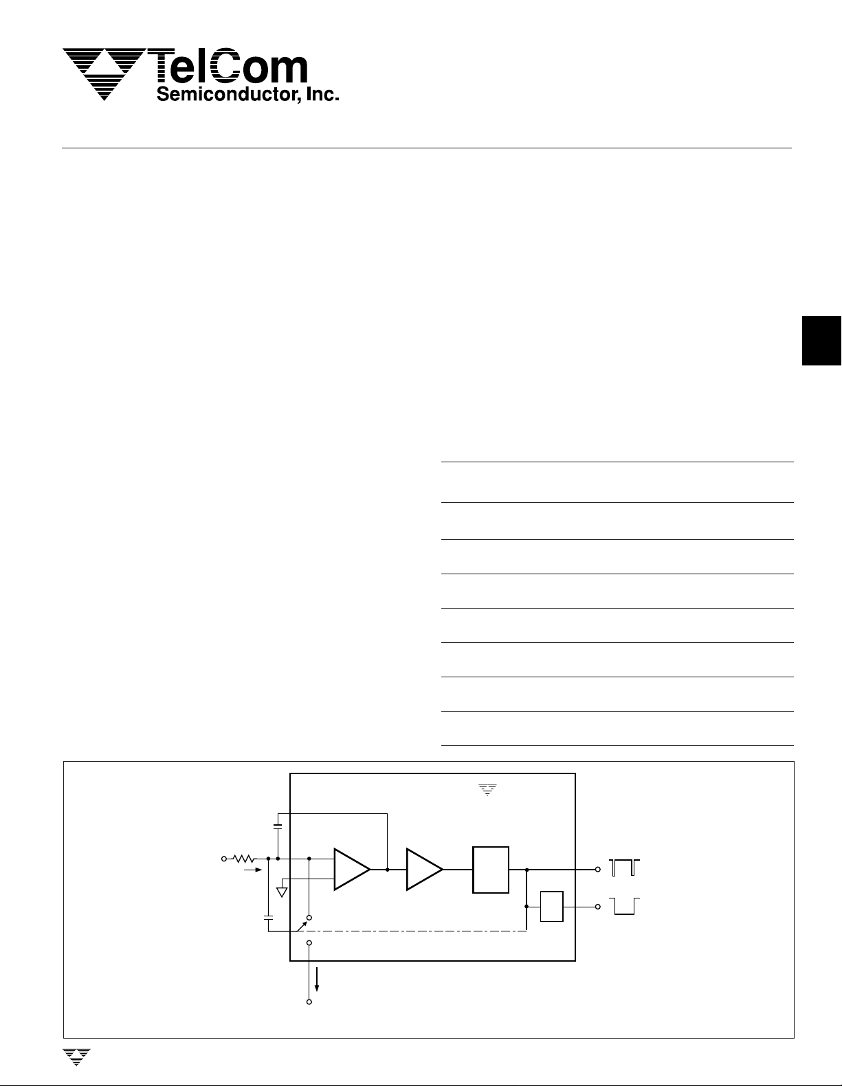
FUNCTIONAL BLOCK DIAGRAM
GENERAL DESCRIPTION
The TC9400/TC9401/TC9402 are low-cost voltage-tofrequency (V/F) converters utilizing low power CMOS
technology. The converters accept a variable analog input
signal and generate an output pulse train whose frequency
is linearly proportional to the input voltage.
The devices can also be used as highly-accurate frequency-to-voltage (F/V) converters, accepting virtually any
input frequency waveform and providing a linearly-proportional voltage output.
A complete V/F or F/V system only requires the addition
of two capacitors, three resistors, and reference voltage.
ORDERING INFORMATION
Linearity Temperature
Part No. (V/F) Package Range
TC9400COD 0.05% 14-Pin 0°C to +70°C
SOIC (Narrow)
TC9400CPD 0.05% 14-Pin 0°C to +70°C
Plastic DIP
TC9400EJD 0.05% 14-Pin – 40°C to +85°C
CerDIP
TC9401CPD 0.01% 14-Pin 0°C to +70°C
Plastic DIP
TC9401EJD 0.01% 14-Pin – 40°C to +85°C
CerDIP
TC9402CPD 0.25% 14-Pin 0°C to +70°C
Plastic DIP
TC9402EJD 0.25% 14-Pin – 40°C to +85°C
CerDIP
2
3
4
5
6
Integrator
Capacitor
R
Input
Voltage
TELCOM SEMICONDUCTOR, INC.
IN
I
IN
Reference
Capacitor
Reference
Voltage
I
REF
Integrator
OpAmp
Threshold
Detector
TC9400
One
Shot
Pulse Output
7
÷2
Pulse/2 Output
8
TC9400/1/2-5 11/6/96
3-287
TC9400
TC9401
TC9402
VOLTAGE-TO-FREQUENCY/
FREQUENCY-TO-VOLTAGE CONVERTERS
ABSOLUTE MAXIMUM RATINGS*
VDD – VSS................................................................. +18V
IIN...........................................................................10mA
V
Max –V
OUT
V
– VSS..............................................................– 1.5V
REF
Storage Temperature Range ................– 65°C to +150°C
Common..........................................23V
OUT
*Static-sensitive device. Unused devices must be stored in conductive
material. Protect devices from static discharge and static fields. Stresses
above those listed under Absolute Maximum Ratings may cause permanent damage to the device. These are stress ratings only and functional
operation of the device at these or any other conditions above those
indicated in the operational sections of the specifications is not implied.
Exposure to Absolute Maximum Rating Conditions for extended periods
may affect device reliability.
Operating Temperature Range
C Device ................................................0°C to +70°C
E Device ...........................................– 40°C to +85°C
Package Dissipation (TA ≤ 70°C)
8-Pin CerDIP ..................................................800mW
8-Pin Plastic DIP.............................................730mW
8-Pin SOIC .....................................................470mW
Lead Temperature (Soldering, 10 sec) .................+300°C
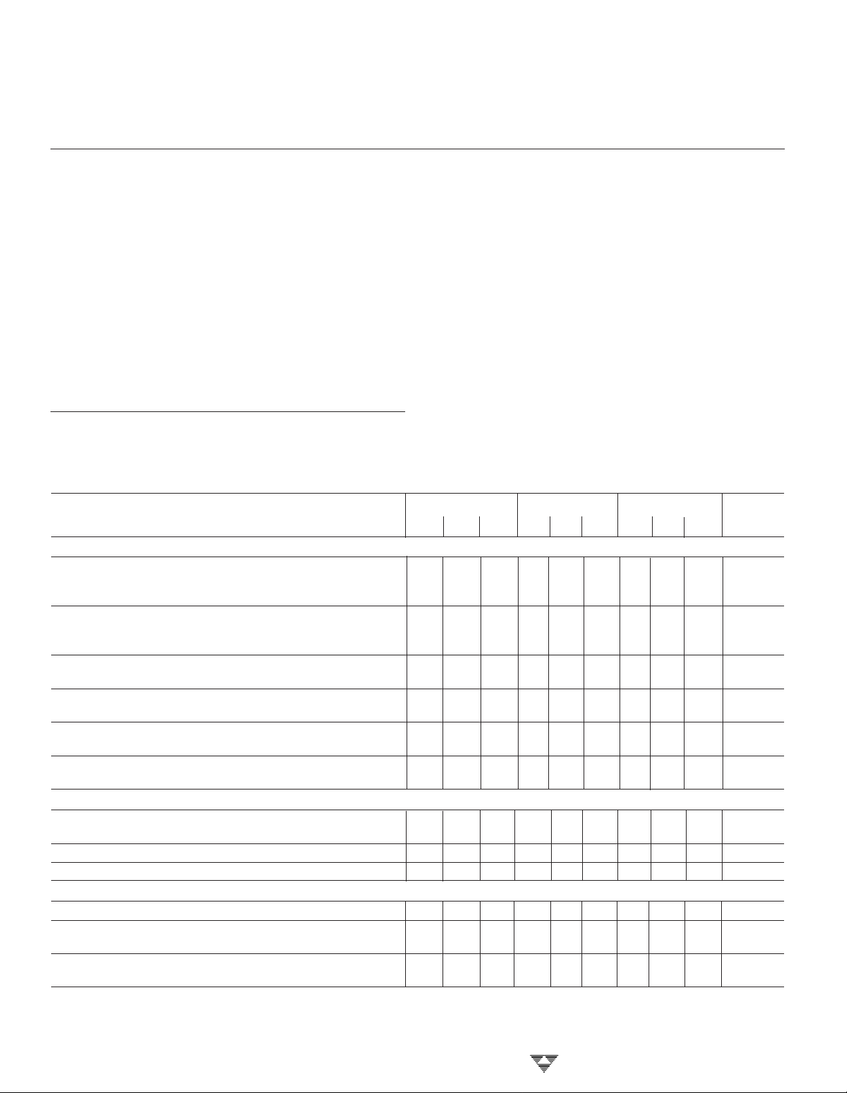
ELECTRICAL CHARACTERISTICS: V
= +5V, VSS = – 5V, V
DD
GND
= 0V, V
= – 5V, R
REF
= 100kΩ,
BIAS
Full Scale = 10kHz, unless otherwise specified. TA = +25°C, unless temperature range is specified (– 40°C to +85°C
for E device, 0°C to +70°C for C device).
VOLTAGE-TO-FREQUENCY TC9401 TC9400 TC9402
Parameter Definition Min Typ Max Min Typ Max Min Typ Max Unit
Accuracy
Linearity 10 kHz Output Deviation From Straight — 0.004 0.01 — 0.01 0.05 — 0.05 0.25 % Full
Line Between Normalized Zero Scale
and Full-Scale Input
Linearity 100 kHz Output Deviation From Straight — 0.04 0.08 — 0.1 0.25 — 0.25 0.5 % Full
Line Between Normalized Zero Scale
Reading and Full-Scale Input
Gain Temperature Variation in Gain A Due to — ± 25 ± 40 — ± 25 ± 40 — ± 50 ± 1 00 ppm/°C
Drift (Note 1) Temperature Change Full Scale
Gain Variance Variation From Ideal Accuracy — ± 10 – — ± 10 — — ± 10 – % of
Nominal
Zero Offset (Note 2) Correction at Zero Adjust for Zero — ± 10 ± 50 — ± 10 ± 50 — ± 20 ± 100 mV
Output When Input is Zero
Zero Temperature Variation in Zero Offset Due to — ± 25 ± 50 — ± 25 ± 50 — ± 50 ± 100 µV/°C
Drift (Note 1) Temperature Change
Analog Input
IIN Full Scale Full-Scale Analog Input Current to — 10 — — 10 — 10 — µA
Achieve Specified Accuracy
IIN Overrange Overrange Current — — 50 — — 50 — — 50 µA
Response Time Settling Time to 0.1% Full Scale — 2 — — 2 — — 2 — Cycle
Digital Section
V
@ IOL = 10mA Logic "0" Output Voltage (Note 3) — 0.2 0.4 — 0.2 0.4 — 0.2 0.4 V
SAT
V
Max – V
OUT
Common (Note 4) and Common
Pulse Frequency — 3 — — 3 — — 3 — µsec
Output Width
OUT
Voltage Range Between Output — — 18 — — 18 — — 18 V
3-288
TELCOM SEMICONDUCTOR, INC.
VOLTAGE-TO-FREQUENCY/
FREQUENCY-TO-VOLTAGE CONVERTERS
1
TC9400
TC9401
TC9402
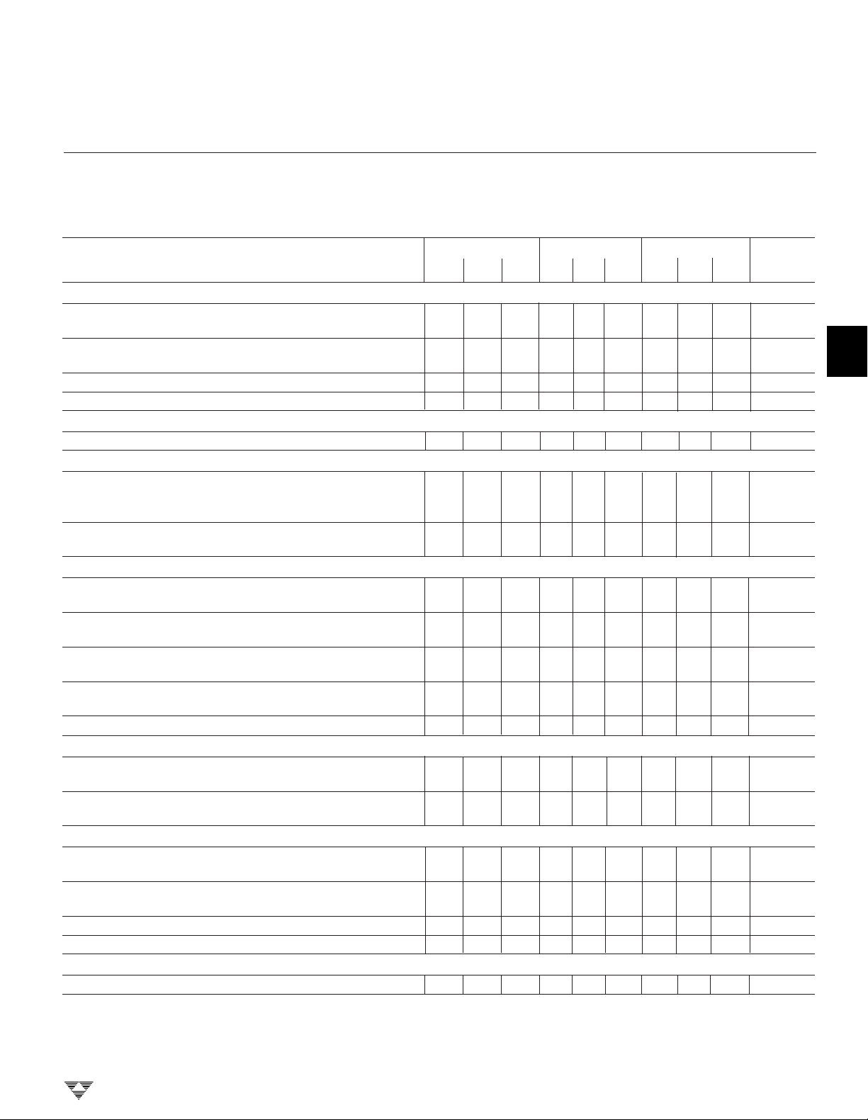
ELECTRICAL CHARACTERISTICS: (Cont.) V
Full Scale = 10kHz, unless otherwise specified. TA = +25°C, unless temperature range is specified – 40°C to +85°C for
E device, 0°C to +70°C for C device.
FREQUENCY-TO-VOLTAGE TC9401 TC9400 TC9402
Parameter Definition Min Typ Max Min Typ Max Min Typ Max Unit
Supply Current
IDD Quiescent Current Required From Positive
(Note 5) Supply During Operation — 1.5 6 — 1.5 6 — 3 10 mA
ISS Quiescent Current Required From Negative
(Note 5) Supply During Operation — – 1.5 – 6 — – 1.5 – 6 – 3 – 10 mA
VDD Supply Operating Range of Positive Supply 4 — 7.5 4 — 7.5 4 — 7.5 V
VSS Supply Operating Range of Negative Supply – 4 — – 7.5 – 4 — – 7.5 – 4 — – 7.5 V
Reference Voltage
V
–V
REF
SS
Accuracy
Nonlinearity (Note 10) Deviation From Ideal Transfer — 0.01 0.02 — 0.02 0.05 — 0.05 0.25 % Full
Input Frequency Frequency Range for Specified 10 — 100k 10 — 100k 10 — 100k Hz
Range (Note 7 and 8) Nonlinearity
Frequency Input
Positive Excursion Voltage Required to Turn 0.4 — V
Negative Excursion Voltage Required to Turn – 0.4 – 2 – 0.4 — – 2 – 0.4 — – 2 V
Minimum Positive Time Between Threshold — 5 — — 5 — — 5 — µsec
Pulse Width (Note 8) Crossings
Minimum Negative Time Between Threshold — 0.5 — — 0.5 — — 0.5 µsec
Pulse Width (Note 8) Crossings
Input Impedance — 10 — — 10 — — 10 — MΩ
Analog Outputs
Output Voltage Voltage Range of Op Amp Output —
(Note 9) for Specified Nonlinearity
Output Loading Resistive Loading at Output of 2 — — 2 — — 2 — — kΩ
Supply Current
IDD Quiescent Current Required From Positive
(Note 10) Supply During Operation — 1.5 6 — 1.5 6 — 3 10 mA
ISS Quiescent Current Required From Negative
(Note 10) Supply During Operation — – 1.5 – 6 – 1.5 – 6 – 3 – 10 mA
VDD Supply Operating Range of Positive Supply 4 — 7.5 4 — 7.5 4 — 7.5 V
VSS Supply Operating Range of Negative Supply – 4 — – 7.5 – 4 — – 7.5 – 4 — – 7.5 V
Reference Voltage
V
–V
REF
SS
NOTES: 1. Full temperature range. Guaranteed, Not Tested.
2. IIN = 0.
3. Full temperature range, I
4. I
= 10µA.
OUT
5. Threshold Detect = 5V, Amp Out = 0V, Full Temperature
Range
TELCOM SEMICONDUCTOR, INC.
Range of Voltage Reference Input – 2.5 — — – 2.5 — — – 2.5 — — V
Function as a Percentage Scale
Full-Scale Voltage
Threshold Detector On
Threshold Detector Off
Op Amp
Range of Voltage Reference Input – 2.5 — — – 2.5 — — – 2.5 — — V
= 10mA.
OUT
= +5V, VSS = – 5V, V
DD
0.4 — V
DD
V
– 1
DD
6. 10Hz to 100kHz.; Guaranteed, Not Tested
7. 5µsec minimum positive pulse width and 0.5 µsec minimum
negative pulse width.
8. tR = tF = 20 nsec.
9. RL ≥ 2kΩ.; Tested @ 10kΩ
10.Full temperature range, VIN = – 0.1V.
——
GND
V
– 1
DD
= 0, V
REF
DD
——
= – 5V, R
0.4 — V
V
– 1
DD
= 100kΩ,
BIAS
DD
—V
V
3-289
2
3
4
5
6
7
8
TC9400
TC9401
TC9402
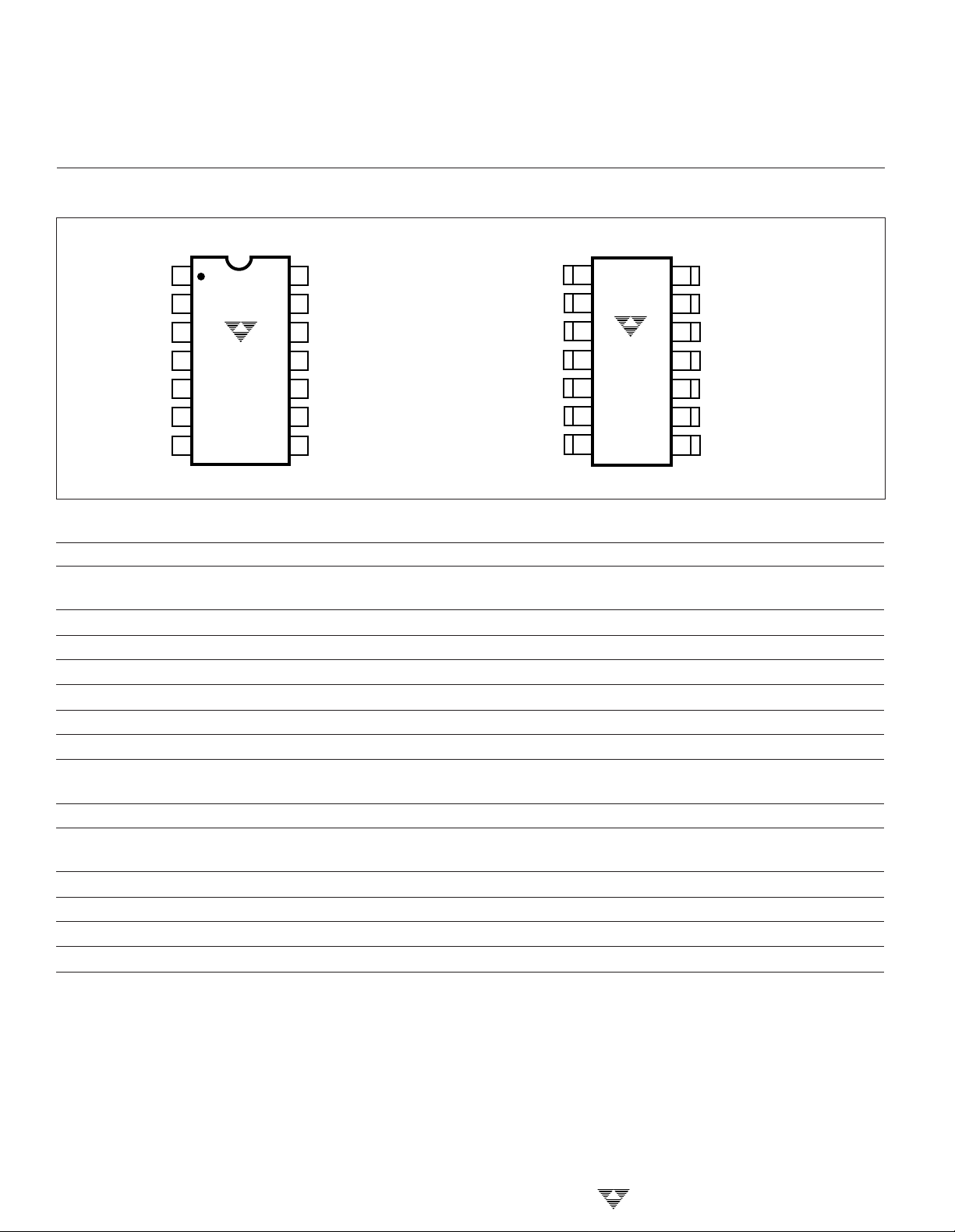
PIN CONFIGURATIONS
14-Pin Plastic DIP/CerDIP 14-Pin SOIC (Narrow)
VOLTAGE-TO-FREQUENCY/
FREQUENCY-TO-VOLTAGE CONVERTERS
I
BIAS
ZERO ADJ
I
V
SS
V
OUT
REF
GND
V
REF
1
2
3
IN
TC9400
4
TC9401
TC9402
5
6
7
V
14
DD
13
NC
12
AMPLIFIER OUT
THRESHOLD DETECTOR
11
FREQ/2 OUT
10
9
OUTPUT COMMON
PULSE FREQ OUT
8
I
BIAS
ZERO ADJ
V
OUT
REF
GND
V
NC = NO INTERNAL CONNECTION
I
IN
V
SS
REF
1
2
3
4
5
6
7
TC9400
TC9401
TC9402
14
V
DD
13
NC
12
AMPLIFIER OUT
11
THRESHOLD DETECTOR
10
FREQ/2 OUT
9
OUTPUT COMMON
8
PULSE FREQ OUT
PIN DESCRIPTIONS
Pin No. Symbol Description
1I
BIAS
2 Zero Adj Low frequency adjustment input. See text.
3I
4V
5V
IN
SS
OUT Reference capacitor connection.
REF
6 GND Analog ground.
7V
REF
8 Pulse Freq Out Frequency output. This open drain output will pulse LOW each time the Freq
9 Output Common Source connection for the open drain output FETs. See text.
10 Freq/2 Out This open drain output is a square wave at one half the frequency of the pulse
11 Threshold Detect Input to the threshold detector. This pin is the frequency input during F/V operation.
12 Amplifier Out Output of the integrator amplifier.
13 NC No internal connection
14 V
DD
This pin sets bias current in the TC9400. Connect to VSS through a 100 kΩ resistor.
See text.
Input current connection for the V/F converter.
Negative power supply voltage connection, typically – 5V.
Voltage reference input, typically – 5V.
threshold detector limit is reached. The pulse rate is proportional to input voltage.
output (pin 8). Output transitions of this pin occur on the rising edge of pin 8.
Positive power supply connection, typically +5V.
3-290
TELCOM SEMICONDUCTOR, INC.

VOLTAGE-TO-FREQUENCY/
FREQUENCY-TO-VOLTAGE CONVERTERS
1
TC9400
TC9401
TC9402
INPUT
V
IN
0V –10V
50kΩ
C
INT
820pF
R
IN
1MΩ
+5V
–5V
OFFSET
ADJUST
510kΩ
11
12
C
REF
180pF
10kΩ
THRESHOLD
DETECT
–3V
AMP OUT
V
REF
5
I
IN
3
ZERO
ADJUST
2
DELAY
THRESHOLD
DETECTOR
SELF-
START
OUT
20kΩ
12pF
60pF
–
OpAmp
+
I
BIAS
1
R
BIAS
100kΩ
–5V
Figure 1. 10 Hz to 10 kHz V/F Converter
+5V
14
V
DD
3µsec
V
SS
4
REFERENCE
VOLTAGE
(TYPICALLY –5V)
V
7
REF
÷2
TC9400
TC9401
TC9402
GND
6
f
OUT
f
/2
OUT
OUTPUT
COMMON
8
10
9
+
5V
2
R
L
10kΩ
+
5V
R
L
10kΩ
3
4
5
6
VOLTAGE-TO-FREQUENCY (V/F) CIRCUIT DESCRIPTION
The TC9400 V/F converter operates on the principal
of charge balancing. The operation of the TC9400 is easily
understood by referring to Figure 1. The input voltage (VIN)
is converted to a current (IIN) by the input resistor. This
current is then converted to a charge on the integrating
capacitor and shows up as a linearly decreasing voltage at
the output of the op amp. The lower limit of the output
swing is set by the threshold detector, which causes the
reference voltage to be applied to the reference capacitor
for a time period long enough to charge the capacitor to
the reference voltage. This action reduces the charge on
the integrating capacitor by a fixed amount (q = C
V
), causing the op amp output to step up a finite
REF
amount.
TELCOM SEMICONDUCTOR, INC.
REF
×
At the end of the charging period, C
is shorted out.
REF
This dissipates the charge stored on the reference capacitor, so that when the output again crosses zero the system
is ready to recycle. In this manner, the continued discharging of the integrating capacitor by the input is balanced out
by fixed charges from the reference voltage. As the input
voltage is increased, the number of reference pulses required to maintain balance increases, which causes the
output frequency to also increase. Since each charge increment is fixed, the increase in frequency with voltage is
linear. In addition, the accuracy of the output pulse width
does not directly affect the linearity of the V/F. The pulse
must simply be long enough for full charge transfer to take
place.
3-291
7
8

TC9400
TC9401
TC9402
f
OUT
VOLTAGE-TO-FREQUENCY/
FREQUENCY-TO-VOLTAGE CONVERTERS
3 µsec
TYP
f
OUT
AMP
OUT
/2
NOTES: 1. To adjust f
2. To adjust f
3. To increase f
4. For high-performance applications, use high-stability components for RIN, C
resistors and glass capacitors). Also, separate output ground (pin 9) from input ground (pin 6).
1/f
, set VIN = 10mV and adjust the 50kΩ offset for 10Hz output.
MIN
, set VIN = 10V and adjust R
MAX
MAX to 100kHz, change C
OUT
Figure 2 . Output Waveforms
The TC9400 contains a "self-start" circuit to ensure the
V/F converter always operates properly when power is first
applied. In the event that, during power-on, the Op Amp
output is below the threshold and C
is already charged,
REF
a positive voltage step will not occur. The op-amp output will
continue to decrease until it crosses the –3.0V threshold of
the "self-start" comparator. When this happens, an internal
resistor is connected to the op-amp input, which forces the
output to go positive until the TC9400 is in its normal
operating mode.
The TC9400 utilizes low power CMOS processing for
low input bias and offset currents with very low power
dissipation. The open-drain N-channel output FETs provide
high voltage and high current sink capability.
V
REF
0V
IN
REF
or V
for 10 kHz output.
REF
to 2pF and C
INT
to 75pF.
REF
, V
(metal film
REF
PIN FUNCTIONS
Threshold Detector Input
In the V/F mode, this input is connected to the amplifier
output (pin 12) and triggers a 3 µsec pulse when the input
voltage passes through its threshold. In the F/V mode, the
input frequency is applied to this input.
The nominal threshold of the detector is halfway between the power supplies, or (VDD + VSS)/2 ±400mV. The
TC9400's charge balancing V/F technique is not dependent
on a precision comparator threshold, because the threshold
only sets the lower limit of the op-amp output. The op-amp's
peak-to-peak output swing, which determines the frequency,
is only influenced by external capacitors and by V
C
C
REF
REF
INT
.
VOLTAGE-TO-TIME MEASUREMENTS
The TC9400 output can be measured in the time domain as well as the frequency domain. Some microcomputers, for example, have extensive timing capability but
limited counter capability. Also, the response time of a time
domain measurement is only the period between two output pulses, while the frequency measurement must accumulate pulses during the entire counter timebase period.
Time measurements can be made from either the
TC9400's Pulse Freq Out output or from the Freq/2 output.
The Freq/2 output changes state on the rising edge of
Pulse Freq Out, so Freq/2 is a symmetrical square wave at
one half the pulse output frequency. Timing measurements
can therefore be made between successive Pulse Freq
Out pulses, or while Freq/2 is high (or low).
3-292
Pulse Freq Out
This output is an open-drain N-channel FET which
provides a pulse waveform whose frequency is proportional
to the input voltage. This output requires a pull-up resistor
and interfaces directly with MOS, CMOS, and TTL logic.
Freq/2 Out
This output is an open-drain N-channel FET which
provides a square wave one-half the frequency of the pulse
frequency output. The Freq/2 output will change state on the
rising edge of Pulse Freq Out. This output requires a pullup resistor and interfaces directly with MOS, CMOS, and
TTL logic.
TELCOM SEMICONDUCTOR, INC.

VOLTAGE-TO-FREQUENCY/
FREQUENCY-TO-VOLTAGE CONVERTERS
1
TC9400
TC9401
TC9402
Output Common
The sources of both the Freq/2 out and the Pulse Freq
Out are connected to this pin. An output level swing from the
drain voltage to ground or to the VSS supply may be obtained
by connecting this pin to the appropriate point.
R
BIAS
An external resistor, connected to VSS, sets the bias
point for the TC9400. Specifications for the TC9400 are
based on R
Increasing the maximum frequency of the TC9400
beyond 100kHz is limited by the pulse width of the Pulse
Output (typically 3µsec). Reducing R
pulse width and increase the maximum operating frequency,
but linearity errors will also increase. R
to 20kΩ, which will typically produce a maximum full scale
frequency of 500kHz.
= 100kΩ ±10%, unless otherwise noted.
BIAS
will decrease the
BIAS
can be reduced
BIAS
Amplifier Out
The output stage of the operational amplifier. During
V/F operation, a negative-going ramp signal is available at
this pin. In the F/V mode, a voltage proportional to the
frequency input is generated.
V
Out
REF
The charging current for C
pin. When the op amp output reaches the threshold level,
this pin is internally connected to the reference voltage and
a charge, equal to V
integrator capacitor. After about 3 µsec, this pin is internally
connected to the summing junction of the op amp to discharge C
the reference voltage is not directly applied to the summing
junction.
. Break-before-make switching ensures that
REF
REF
x C
is supplied through this
REF
, is removed from the
REF
V/F CONVERTER DESIGN INFORMATION
Input/Output Relationships
The output frequency (f
voltage (VIN) by the transfer equation:
Frequency out = ×
V
R
) is related to the analog input
OUT
(V
REF
1
) (C
REF
)
IN
IN
External Component Selection
R
IN
The value of this component is chosen to give a fullscale input current of approximately 10µA:
2
3
4
Zero Adjust
This pin is the noninverting input of the operational
amplifier. The low-frequency set point is determined by
adjusting the voltage at this pin.
I
IN
The inverting input of the operational amplifier and the
summing junction when connected in the V/F mode. An
input current of 10µA is specified, but an overrange current
up to 50µA can be used without detrimental effect to the
circuit operation. IIN connects the summing junction of an
operational amplifier. Voltage sources cannot be attached
directly, but must be buffered by external resistors.
V
REF
A reference voltage from either a precision source or the
VSS supply is applied to this pin. Accuracy of the TC9400 is
dependent on the voltage regulation and temperature characteristics of the reference circuitry.
Since the TC9400 is a charge balancing V/F converter,
the reference current will be equal to the input current. For
this reason, the DC impedance of the reference voltage
source must be kept low enough to prevent linearity errors.
For linearity of 0.01%, a reference impedance of 200Ω or
less is recommended. A 0.1µF bypass capacitor should be
connected from V
TELCOM SEMICONDUCTOR, INC.
to ground.
REF
REF
≤ 4C
VIN Full Scale
10µA
RIN ≅ = 1MΩ.
≤ C
REF
10V
10µA
≤ 10 C
INT
. Low-leakage types are recommended,
REF
.
REF
3-293
by
RIN ≅ .
Example:
Note that the value is an approximation and the exact
relationship is defined by the transfer equation. In practice,
the value of RIN typically would be trimmed to obtain fullscale frequency at VIN full scale (see "Adjustment Procedure"). Metal film resistors with 1% tolerance or better are
recommended for high-accuracy applications because of
their thermal stability and low-noise generation.
C
INT
The exact value is not critical but is related to C
the relationship:
3C
Improved stability and linearity are obtained when
C
INT
although mica and ceramic devices can be used in applications where their temperature limits are not exceeded.
Locate as close as possible to pins 12 and 13.
5
6
7
8

TC9400
TC9401
TC9402
C
REF
The exact value is not critical and may be used to trim the
full-scale frequency (see "Input/Output Relationships"). Glass
film or air trimmer capacitors are recommended because of
their stability and low leakage. Locate as close as possible
to pins 5 and 3.
VDD, V
SS
Power supplies of ±5V are recommended. For highaccuracy requirements, 0.05% line and load regulation and
0.1µF disc decoupling capacitors located near the pins are
recommended.
Adjustment Procedure
Figure 1 shows a circuit for trimming the zero location.
Full scale may be trimmed by adjusting RIN, V
Recommended procedure for a 10kHz full-scale frequency
is as follows:
(1) Set VIN to 10 mV and trim the zero adjust circuit to
obtain a 10Hz output frequency.
REF
, or C
REF
VOLTAGE-TO-FREQUENCY/
FREQUENCY-TO-VOLTAGE CONVERTERS
Improved Single Supply V/F Converter
Operation
A TC9400 which operates from a single 12 to 15V
variable power source is shown in Figure 5. This circuit uses
two Zener diodes to set stable biasing levels for the TC9400.
The Zener diodes also provide the reference voltage, so the
output impedance and temperature coefficient of the Zeners
will directly affect power supply rejection and temperature
performance.
Full scale adjustment is accomplished by trimming the
input current. Trimming the reference voltage is not recommended for high accuracy applications unless an op amp is
used as a buffer, because the TC9400 requires a low
impedance reference (see the V
for more information).
.
The circuit of Figure 5 will directly interface with CMOS
logic operating at 12V to 15V. TTL or 5V CMOS logic can be
accommodated by connecting the output pullup resistors to
the +5V supply. An optoisolator can also be used if an
isolated output is required.
pin description section
REF
(2) Set VIN to 10V and trim either RIN, V
REF
, or C
REF
to
obtain a 10kHz output frequency.
If adjustments are performed in this order, there should be
no interaction and they should not have to be repeated.
500
400
300
(pF) +12pF
200
REF
C
100
0 –1
1 kHz
100kHz
–2 –3 –4 –5 –6 –7
V
REF
(V)
V
= +5V
DD
VSS = – 5V
RIN = 1MΩ
VIN = +10V
TA = +25°C
3-294
Figure 3. Recommended C
REF
vs V
REF
TELCOM SEMICONDUCTOR, INC.

VOLTAGE-TO-FREQUENCY/
FREQUENCY-TO-VOLTAGE CONVERTERS
V+ = 8V TO 15V (FIXED)
1
TC9400
TC9401
TC9402
0.9
R
1
8.2
kΩ
2
kΩ
IN
R
1
1 MΩ
1.4 MΩ
2 MΩ
Figure 4 . Fixed Voltage — Single Supply Operation
R4
R5
91k
Rp
20k
ANALOG GROUND
R1
910k
R2
910k
INPUT
VOLTAGE
(0 to 10V)
V
IN
0V–10V
GAIN
ADJUST
OFFSET
ADJUST
R
1MΩ
V
10V
12V
15V
R3
GAIN
100k
OFFSET
+
100k
COMPONENT SELECTION
F/S FREQ.
1 kHz
10 kHz
100 kHz
CREF
2200pF
180pF
27pF
CINT
4700pF
470pF
75pF
5V
0.2
R
1
820
pF
R
2
V
2
2
6
0.01
µF
7
V
REF
11
0.01
µF
12
180
pF
I
IN
100 kΩ
R
2
10kΩ
14kΩ
20kΩ
5.1VZ
5.1VZ
1µF
D2
D1
f
OUT
1.2k*
C
INT
0.1µ
100k
Figure 5. Voltage to Frequency
TC9400
5
3
I
IN
149
= I
×
IN
(VIN–V2) (V+–V2)
=
I
IN
R
IN
11
12
C
5
REF
3
2
6
7
1
14
1
–
(V
V7) (C
2
+
(0.9 R1+0.2 R1)
+12 to +15V
V
DD
THRESHOLD
DETECT
AMP OUT
C
REF
TC9400
I
IN
ZERO
ADJUST
GND
V
REF
I
BIAS
V
SS
8
10
)
REF
14
f
OUT
f
OUT
OUTPUT
COMMON
4
10kΩ
8
10
/2
9
10kΩ
f
OUT
f
OUT
10k 10k
/2
OUTPUT
FREQUENCY
DIGITAL
GROUND
2
3
4
5
6
7
8
TELCOM SEMICONDUCTOR, INC.
3-295

TC9400
TC9401
TC9402
VOLTAGE-TO-FREQUENCY/
FREQUENCY-TO-VOLTAGE CONVERTERS
FREQUENCY-TO-VOLTAGE (F/V) CIRCUIT DESCRIPTION
When used as an F/V converter, the TC9400 generates
an output voltage linearly proportional to the input frequency
waveform.
Each zero crossing at the threshold detector's input
causes a precise amount of charge (q = C
REF
× V
REF
) to be
dispensed into the op amp's summing junction. This charge
in turn flows through the feedback resistor, generating
voltage pulses at the output of the op amp. A capacitor (C
across R
averages these pulses into a DC voltage which
INT
INT
is linearly proportional to the input frequency.
F/V CONVERTER DESIGN INFORMATION
Input/Output Relationships
The output voltage is related to the input frequency (fIN)
by the transfer equation:
V
= [V
OUT
REF CREF RINT
The response time to a change in fIN is equal to (R
C
). The amount of ripple on V
INT
to C
and the input frequency.
INT
C
can be increased to lower the ripple. Values of 1µF
INT
to 100µF are perfectly acceptable for low frequencies.
When the TC9400 is used in the single-supply mode,
V
is defined as the voltage difference between pin 7 and
REF
pin 2.
] fIN.
is inversely proportional
OUT
INT
Input Voltage Levels
The input frequency is applied to the Threshold Detector
input (Pin 11). As discussed in the V/F circuit section of this
data sheet, the threshold of pin 11 is approximately (VDD +
VSS) /2 ±400mV. Pin 11's input voltage range extends from
VDD to about 2.5 V below the threshold. If the voltage on pin
11 goes more than 2.5 volts below the threshold, the V/F
mode startup comparator will turn on and corrupt the output
voltage. The Threshold Detector input has about 200 mV of
hysteresis.
)
In ±5 V applications, the input voltage levels for the
TC9400 are ±400mV, minimum. If the frequency source
being measured is unipolar, such as TTL or CMOS operating from a +5V source, then an AC coupled level shifter
should be used. One such circuit is shown in Figure 6a.
The level shifter circuit in Figure 6b can be used in single
supply F/V applications. The resistor divider ensures that
the input threshold will track the supply voltages. The diode
clamp prevents the input from going far enough in the
negative direction to turn on the startup comparator. The
diode's forward voltage decreases by 2.1 mV/°C, so for high
ambient temperature operation two diodes in series are
recommended.
3-296
Frequency
Input
+5V
0V
0.01µF
33k
(A) ±5V Supply
IN914
+5V
14
V
DD
TC9400
11
DET
1.0M
GND
Figure 6. Frequency Input Level Shifter
V
64
–5V
SS
Frequency
Input
+5V
0V
0.01µF
33k
(B) Single Supply
TELCOM SEMICONDUCTOR, INC.
IN914
0.1µF
10k
10k
11
1.0M
+8V to +5V
TC9400
DET
14
V
DD
V
SS
4

(
)
VOLTAGE-TO-FREQUENCY/
FREQUENCY-TO-VOLTAGE CONVERTERS
TC9400
1
TC9401
TC9402
f
IN
–5V
2 kΩ
SEE
FIGURE
6
OFFSET
ADJUST
+5V
100kΩ
2.2kΩ
TC9400A
TC9401A
TC9402A
THRESHOLD
DETECT
ZERO ADJUST
2
I
BIAS
11
THRESHOLD
DETECTOR
14
10 kΩ
3 µsec
DELAY
V
SS
Figure 7. DC — 10 kHz F/V Converter
V
7
+5V
14
V
DD
42
–
AMP
+
REF
V
REF
TYPICALLY –5V
OP
OUTPUT
COMMON
12pF
60pF
GND
6
f
OUT/2
f
OUT
V
REF
OUT
AMP
OUT
10
9
8
5
I
IN
3
12
+
V
*
+
V
*
*
* OPTIONAL
IF BUFFER
IS NEEDED
C
REF
56 pF
R
INT
1 MΩ
SEE
EQUATION,
PAGE 12
C
INT
+
1000pF
V
2
3
4
O
5
6
0.5µsec
MIN
INPUT
f
OUT
f
OUT
DELAY = 3µsec
/2
Figure 8 . F/V Digital Outputs
5.0µsec
MIN
TELCOM SEMICONDUCTOR, INC.
Input Buffer
f
OUT
and f
/2 are not used in the F/V mode. However,
OUT
these outputs may be useful for some applications, such as
a buffer to feed additional circuitry. Then, f
input frequency waveform, except that f
3µsec after fIN goes high; f
frequency of one-half f
OUT
/2 will be squarewave with a
OUT
.
will follow the
OUT
will go high
OUT
7
If these outputs are not used, pins 8, 9 and 10 should be
connected to ground.
8
3-297

TC9400
1M
47pF
V
OUT
TC9400
12
3
5
V
REF
OUT
I
IN
GND
AMP OUT
6
.001µF
+
–
1M
3
2
.01µF
1M
0.1µF
+5
7
6
4
–5
TL071
200
TC9401
TC9402
VOLTAGE-TO-FREQUENCY/
FREQUENCY-TO-VOLTAGE CONVERTERS
V+ = 10V to 15V
100k
Frequency
Input
Offset
Adjust
33k
10k
6.2V
500k
0.01µF
.01µF
IN914
0.1µF
V
10k
+
1.0k
1.0k
1.0M
6
2
11
GND
TC9400
ZERO
ADJUST
DET
I
BIAS
100k
14
V
DD
V
AMP OUT
V
REF
7
REF
V
OUT
GND
SS
4
5
47pF
3
I
IN
.001µF
1M
12
V
6
OUT
Note: The output is referenced to pin 6, which is at 6.2V (Vz). For frequency meter applications,
a 1 mA meter with a series-scaling resistor can be placed across pins 6 and 12.
Figure 9. F/V Single Supply F/V Converter
Output Filtering
The output of the TC9400 has a sawtooth ripple superimposed on a DC level. The ripple will be rejected if the
TC9400 output is converted to a digital value by an integrating analog to digital converter, such as the TC7107 or
TC7109. The ripple can also be reduced by increasing the
value of the integrating capacitor, although this will reduce
the response time of the F/V converter.
eliminated without affecting the F/V's response time by
using the circuit in Figure 10. The circuit is a capacitance
multiplier, where the output coupling capacitor is multiplied
by the AC gain of the op amp. A moderately fast op amp,
such as the TL071, should be used.
3-298
The sawtooth ripple on the output of an F/V can be
Figure 10. Ripple Filter
TELCOM SEMICONDUCTOR, INC.

VOLTAGE-TO-FREQUENCY/
FREQUENCY-TO-VOLTAGE CONVERTERS
1
TC9400
TC9401
TC9402
F/V POWER-ON RESET
In F/V mode, the TC9400 output voltage will occasionally be at its maximum value when power is first applied. This
condition remains until the first pulse is applied to fIN. In most
frequency-measurement applications this is not a problem,
because proper operation begins as soon as the frequency
input is applied.
1000pF
f
IN
V
DD
1kΩ
In some cases, however, the TC9400 output must be
zero at power-on without a frequency input. In such cases,
a capacitor connected from pin 11 to VDD will usually be
sufficient to pulse the TC9400 and provide a power-on reset
(see Figure 11A). Where predictable power-on operation is
critical, a more complicated circuit, such as Figure 11B, may
be required.
V
DD
14
THRESHOLD
11
DETECTOR
(A)
TC9400
2
3
4
100kΩ
1µF
3
4
12516
V
CC
CLRA
A
Figure 11. Power-On Operation/Reset
B R C
CD4538
V
SS
8
Q
(B)
5
6
To TC 9400
f
IN
6
7
TELCOM SEMICONDUCTOR, INC.
8
3-299
 Loading...