

TelCom Semiconductor Inc TC913BCPA, TC913BCOA, TC913ACPA, TC913ACOA Datasheet

DUAL AUTO-ZEROED OPERA TIONAL AMPLIFIERS
1
TC913A
TC913B
FEATURES
■ First Monolithic Dual Auto-Zeroed Operational
Amplifier
■ Chopper Amplifier Performance Without External
Capacitors
—VOS........................................................ 15µV Max
—VOS Drift ....................................... 0.15µV/ °C Max
— Saves Cost/Assembly of Four "Chopper"
Capacitors
■ SOIC Packages Available
■ High DC Gain ................................................. 120dB
■ Low Supply Current ...................................... 650µA
■ Low Input Voltage Noise
(0.1 Hz to 10 Hz) ........................................0.65µV
P-P
■ Wide Common-Mode
Voltage Range................................. VSS to VDD – 2V
■ High Common-Mode Rejection .................... 116dB
■ Dual or Single Supply Operation ....±3.3V to ±8.3V
+6.5V to +16V
■ Excellent AC Operating Characteristics
— Slew Rate ............................................. 2.5V/µsec
— Unity-Gain Bandwidth .............................1.5MHz
■ Pin Compatible With LM358, OP-14, MC1458,
ICL7621, TL082, TLC322
ORDERING INFORMATION
Maximum
Temp. Offset
Part No. Package Range Voltage
TC913ACOA 8-Pin SOIC 0°C to +70°C15µV
TC913ACPA 8-Pin Plastic DIP 0°C to +70°C15µV
TC913BCOA 8-Pin SOIC 0°C to +70°C30µV
TC913BCPA 8-Pin Plastic DIP 0°C to +70°C30µV
PIN CONFIGURATION (SOIC and DIP)
V
DD
8OUT A
B
7
OUT B
–
6
–IN B
5
+IN B
–IN A
+IN A
V
SS
1
–
2
3
4
TC913ACPA
TC913BCPA
A
+
8OUT A
V
B
+
DD
7
OUT B
–
6
–IN B
+IN B
5
–IN A
+IN A
V
SS
TELCOM SEMICONDUCTOR, INC.
1
–
2
3
4
TC913ACOA
TC913BCOA
A
+
+
GENERAL DESCRIPTION
The TC913 is the world's first complete monolithic,
dual auto-zeroed operational amplifier. The TC913 sets a
new standard for low-power, precision dual-operational
amplifiers. Chopper-stabilized or auto-zeroed amplifiers
offer low offset voltage errors by periodically sampling
offset error, and storing correction voltages on capacitors.
Previous single amplifier designs required two user-supplied, external 0.1µF error storage correction capacitors —
much too large for on-chip integration. The unique TC913
architecture requires smaller capacitors, making on-chip
integration possible. Microvolt offset levels are achieved
and external capacitors are not required.
The TC913 system benefits are apparent when contrasted with a TC7650 chopper amplifier circuit implementation. A single TC913 replaces two TC7650's and four
capacitors. Five components and assembly steps are eliminated.
The TC913 pinout matches many popular dualoperational amplifiers: OP-04, TLC322, LM358, and
ICL7621 are typical examples. In many applications,
operating from dual 5V power supplies or single supplies,
the TC913 offers superior electrical performance, and can
be a functional drop-in replacement; printed circuit board
rework is not necessary. The TC913's low offset voltage
error eliminates offset voltage trim potentiometers often
needed with bipolar and low-accuracy CMOS operational
amplifiers.
The TC913 takes full advantage of TelCom's proprietary CMOS technology. Unity gain bandwidth is 1.5 MHz
and slew rate is 2.5 V/µsec.
FUNCTIONAL BLOCK DIAGRAM
V
DD
V CORRECTION AMPLIFIER
OS
+
–
*
–
+
MAIN
AMPLIFIER
B
*
LOW IMPEDANCE
OUTPUT BUFFER
+
–
A
INTERNAL
OSCILLATOR
≈
(f 200 Hz)
OSC
B
TC913
OUTPUT A
1
OUTPUT B
7
TC913A/B-89/3/96
3-269
–INPUT A
–INPUT B
–INPUT A
–INPUT B
V
SS
A
2
6
5
3
1 OF 2 AMPLIFIERS SHOWN
*NOTE: Internal capacitors. No external capacitors required.
48
2
3
4
5
6
7
8
TC913A
TC913B
DUAL AUTO-ZEROED
OPERA TIONAL AMPLIFIERS
ABSOLUTE MAXIMUM RATINGS*
Total Supply Voltage (VDD to VSS ) .......................... +18V
Input Voltage ........................ (V
Current into Any Pin .................................................10mA
While Operating................................................100µA
Storage Temperature Range ................– 65°C to +150°C
Lead Temperature (Soldering, 10 sec) .................+300°C
Operating Temperature Range
+ 0.3V) to (VSS – 0.3V)
DD
Package Power Dissipation (TA = ≤ 70°C)
Plastic SOIC ...................................................470mW
Plastic DIP ......................................................730mW
*Static-sensitive device. Unused devices should be stored in conductive
material. Stresses above those listed under “Absolute Maximum Ratings”
may cause permanent damage to the device. These are stress ratings only
and functional operation of the device at these or any other conditions
above those indicated in the operational sections of the specifications is not
implied.
C Device ................................................0°C to +70°C
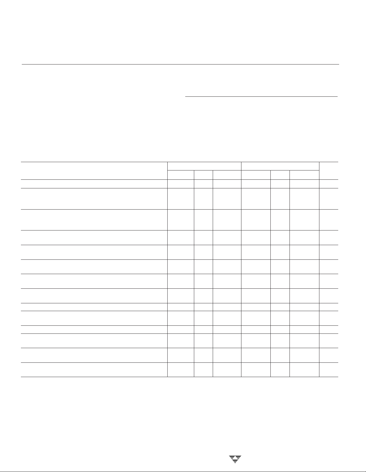
ELECTRICAL CHARACTERISTICS: V
= ±5V, TA = +25°C, unless otherwise indicated.
S
TC913A TC913B
Symbol Parameter Test Conditions Min Typ Max Min Typ Max Unit
V
OS
TCV
I
B
IOSAverage Input TA = +25°C — 5 20 — 10 40 pA
e
N
CMRR Common-Mode VSS ≤ VCM ≤ V
CMVR Common-Mode V
A
OL
V
OUT
BW Closed-Loop Closed Loop Gain = +1 — 1.5 — — 1.5 — MHz
SR Slew Rate RL = 10 kΩ, CL = 50 pF — 2.5 — — 2.5 — V/µs
PSRR Power Supply ±3.3V ≤ VS ≤ ±5.5V 110 — — 100 — — dB
V
S
I
S
NOTE: 1. Characterized; not 100% tested.
Input Offset Voltage TA = +25°C — 5 15 — 15 30 µV
Average Temperature 0°C ≤ TA ≤ +70°C — 0.05 0.15 — 0.1 0.25 µV/°C
OS
Coefficient of Input –25°C ≤ T
≤ +85°C — 0.05 0.15 — 0.1 0.25 µV/°C
A
Offset Voltage (Note 1)
Average Input Bias TA = +25°C — — 90 — — 120 pA
Current 0°C ≤ T
≤ +70°C——3——4nA
A
–25°C ≤ TA ≤ +85°C——4——6nA
Offset Current TA = +85°C——1——1nA
Input Voltage Noise 0.1 to 1 Hz, RS ≤ 100Ω — 0.6 — — 0.6 — µV
0.1 to 10 Hz, RS ≤ 100Ω —11— — 11—µV
– 2.2V 110 116 — 100 110 — dB
DD
P-P
P-P
Rejection Ratio
SS
—VDD – 2 V
SS
—VDD – 2 V
Voltage Range
Open-Loop Voltage RL = 10 kΩ, VO = ±4V 115 120 — 110 120 — dB
Gain
Output Voltage Swing RL = 10 kΩ VSS + 0.3 — VDD – 0.9 VSS + 0.3 — VDD – 0.9 V
Bandwidth
Rejection Ratio
Operating Supply Split Supply ±3.3 — ±8.3 ±3.3 — ±8.3 V
Voltage Range Single Supply 6.5 — 16 6.5 — 16 V
Quiescent Supply VS = ±5V — 0.65 0.85 — — 1.1 mA
Current
3-270
TELCOM SEMICONDUCTOR, INC.
 Loading...