

TelCom Semiconductor Inc TC911BCPA, TC911BCOA, TC911ACPA, TC911ACOA Datasheet
AUTO-ZEROED OPERATIONAL AMPLIFIERS
FEATURES
■ First Monolithic Chopper-Stabilized Amplifier
With On-Chip Nulling Capacitors
■ Offset Voltage .................................................... 5µV
■ Offset Voltage Drift .................................. 0.05µV/°C
■ Low Supply Current ...................................... 350µA
■ High Common-Mode Rejection .................... 116dB
■ Single Supply Operation.......................4.5V to 16V
■ High Slew Rate............................................. 2.5V/µs
■ Wide Bandwidth............................................1.5MHz
■ High Open-Loop Voltage Gain
(RL = 10 kΩ) .................................................... 120dB
■ Low Input Voltage Noise
(0.1 Hz to 1 Hz).......................................... 0.65µV
P-P
■ Pin Compatible With ICL7650
■ Lower System Parts Count
ORDERING INFORMATION
Maximum
Temperature Offset
Part No. Package Range Voltage
TC911ACOA 8-Pin SOIC 0°C to +70°C15µV
TC911ACPA 8-Pin 0°C to +70°C15µV
Plastic DIP
TC911BCOA 8-Pin SOIC 0°C to +70°C30µV
TC911BCPA 8-Pin 0°C to +70°C30µV
Plastic DIP
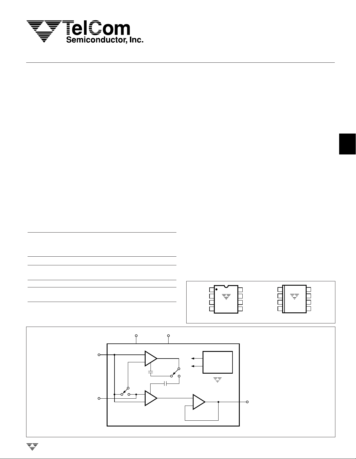
FUNCTIONAL BLOCK DIAGRAM
V
SS
V CORRECTION AMPLIFIER
OS
*
*
MAIN
AMPLIFIER
–INPUT
+INPUT
V
DD
47
2
A
3
+
–
+
–
GENERAL DESCRIPTION
The TC911 CMOS auto-zeroed operational amplifier is
the first complete monolithic chopper-stabilized amplifier.
Chopper operational amplifiers like the ICL7650/7652 and
LTC1052 require user-supplied, external offset compensation storage capacitors. External capacitors are not re-
quired with the TC911. Just as easy to use as the conventional OP07 type amplifier, the TC911 significantly reduces
offset voltage errors. Pinout matches the OP07/741/7650
8-pin mini-DIP configuration.
Several system benefits arise by eliminating the external chopper capacitors: lower system parts count, reduced
assembly time and cost, greater system reliability, reduced
PC board layout effort and greater board area utilization.
Space savings can be significant in multiple-amplifier designs.
Electrical specifications include 15µV maximum offset
voltage, 0.15µV/°C maximum offset voltage temperature
coefficient. Offset voltage error is five times lower than the
premium OP07E bipolar device. The TC911 improves offset drift performance by eight times.
The TC911 operates from dual or single power supplies. Supply current is typically 350µA. Single 4.5V to 16V
supply operation is possible, making single 9V battery
operation possible. The TC911 is available in 2 package
types: 8-pin plastic DIP and SOIC.
PIN CONFIGURATION (SOIC and DIP)
1
NC
2
– INPUT
3
+ INPUT
A
B
B
+
–
TC911ACPA
TC911BCPA
V
4
SS
INTERNAL
OSCILLATOR
(f 200 Hz)
≈
OSC
TC911
LOW IMPEDANCE
OUTPUT BUFFER
1
8
NC
V
7
DD
6
OUTPUT
NC
5
NC = NO INTERNAL CONNECTION
6
OUTPUT
NC
– INPUT
+ INPUT
V
2
3
SS
4
TC911A
TC911B
TC911ACOA
TC911BCOA
8
7
6
5
NC
V
DD
OUTPUT
NC
1
2
3
4
5
6
7
*
NOTE: Internal capacitors. No external capacitors required.
TELCOM SEMICONDUCTOR, INC.
8
TC911/A/B-7 9/11/96
3-263
TC911A
TC911B
AUTO-ZEROED MONOLITHIC
OPERA TIONAL AMPLIFIERS
ABSOLUTE MAXIMUM RATINGS*
Package Power Dissipation (TA = ≤ 70°C)
Plastic DIP ......................................................730mW
Total Supply Voltage (VDD to VSS) ........................... +18V
Input Voltage ........................ (V
+ 0.3V) to (VSS – 0.3V)
DD
Current into Any Pin .................................................10mA
While Operating................................................100µA
Storage Temperature Range ................– 65°C to +150°C
Lead Temperature (Soldering, 10 sec) .................+300°C
Operating Temperature Range
Plastic SOIC ...................................................470mW
*Static-sensitive device. Unused devices should be stored in conductive
material. Stresses above those listed under “Absolute Maximum Ratings”
may cause permanent damage to the device. These are stress ratings only
and functional operation of the device at these or any other conditions
above those indicated in the operational sections of the specifications is not
implied.
C Device ................................................ 0°C to +70°C
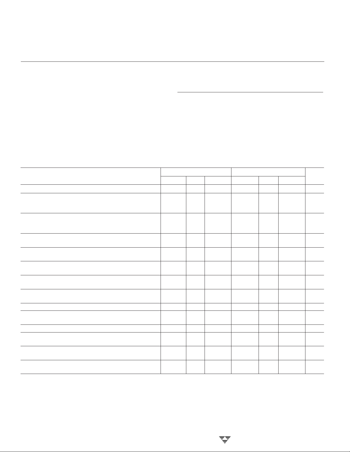
ELECTRICAL CHARACTERISTICS: V
= ±5V, TA = +25°C, unless otherwise indicated.
S
TC911A TC911B
Symbol Parameter Test Conditions
V
OS
TCV
I
B
IOSAverage Input TA = +25°C — 5 20 — 10 40 pA
e
N
CMRR Common-Mode VSS ≤ VCM ≤ VDD – 2.2 110 116 — 105 110 — dB
CMVR Common-Mode V
A
OL
V
OUT
BW Closed Loop Closed Loop Gain = +1 — 1.5 — — 1.5 — MHz
SR Slew Rate RL = 10 kΩ, CL = 50 pF — 2.5 — — 2.5 — V/µs
PSRR Power Supply ±3.3V to ±5.5V 112 — — 105 — — dB
V
S
I
S
NOTES: 1. Characterized; not 100% tested.
Input Offset Voltage TA = +25°C — 5 15 — 15 30 µV
Average Temperature 0°C ≤ TA ≤ +70°C — 0.05 0.15 — 0.1 0.25 µV/°C
OS
Coefficient of Input –25°C ≤ T
≤ +85°C — 0.05 0.15 — 0.1 0.25 µV/°C
A
Offset Voltage (Note 1)
Average Input Bias TA = +25°C — — 70 — — 120 pA
Current 0°C ≤ T
≤ +70°C——3——4nA
A
–25°C ≤ TA ≤ +85°C——4 ——6nA
Offset Current TA = +85°C——1——1nA
Input Voltage Noise 0.1 to 1 Hz, RS ≤ 100Ω — 0.65 — — 0.65 — µV
0.1 to 10 Hz, RS ≤ 100Ω —11— — 11—µV
Rejection Ratio
Voltage Range
Open-Loop Voltage
RL = 10 kΩ, V
OUT
= ±4V
Gain
Output Voltage Swing RL = 10 kΩ VSS + 0.3 — VDD – 0.9 VSS + 0.3 — VDD – 0.9 V
Bandwidth
Rejection Ratio
Operating Supply Split Supply ±3.3 — ± 8 ±3.3 — ±8V
Voltage Range Single Supply 6.5 — 16 6.5 — 16 V
Quiescent Supply VS = ±5V — 350 600 — — 800 µA
Current
Min Typ Max Min Typ Max Unit
P-P
P-P
SS
—V
115 120 — 110 120 — dB
– 2 V
DD
SS
—V
DD
– 2 V
3-264
TELCOM SEMICONDUCTOR, INC.
 Loading...