

TelCom Semiconductor Inc TC901CPA, TC901COA Datasheet
MONOLITHIC, AUT O-ZEROED OPERATIONAL AMPLIFIER
1
TC901
FEATURES
■ Second-Generation Monolithic,
Chopper-Stabilized Op Amp
■ No External Capacitors Required
■ Single-Supply Operation ........... ±15V or 5V to 32V
■ Supply Current............................450µA at 15V, Typ
■ Input Offset Voltage ...................................7µV, Typ
■ Common-Mode Rejection Ratio ............140dB, Typ
■ Open-Loop Gain ............ 140dB Into 10k Load, Typ
■ Input Noise ......................... 5µV at 10Hz Bandwidth
■ Pinout Compatible With ICL7650
■ Lowest Parts Count Chopper Op Amp
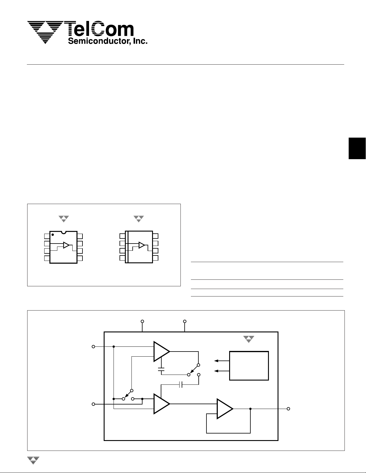
PIN CONFIGURATION (DIP and SOIC)
NC
–INPUT
+INPUT
V
SS
TC901CPA
1
2
3
4
8
–
+
NC
DD
–INPUT
+INPUT
7
V
6
OUTPUT
NC
5
NC = NO INTERNAL CONNECTION
V
NC
SS
TC901COA
1
2
3
4
8
–
+
NC
V
7
OUTPUT
6
NC
5
DD
GENERAL DESCRIPTION
The TC901 is a monolithic, auto-zeroed operational
amplifier. It is a second-generation design of the TC91X
CMOS chopper-stabilized op amps with on-chip capacitors.
Elimination of the external capacitors allows the designer to increase reliability, lower cost, and simplify design
by lowering parts count.
Since the TC901 is an auto-zeroing op amp, input offset
voltage is very low. More important, there is almost zero drift
with time. This eliminates production line adjustments, as
well as periodic calibration.
Notable electrical characteristics are low supply current (450µA, typical), single-supply operation (5V to 32V),
low input offset voltage (7µV, typical), low noise (<5µV
P-P
typical, for a 10Hz bandwidth), and fast recovery from
saturation without the use of external clamp circuitry.
This device is supplied in 8-pin plastic DIP and plastic
SOIC packages. It is pin compatible with bipolar, CMOS,
JFET and other chopper-stabilized op amps using the
industry-standard 741 pinout.
ORDERING INFORMATION
Temperature
Part No. Package Range
TC901COA 8-Pin SOIC 0°C to +70°C
TC901CPA 8-Pin Plastic DIP 0°C to +70°C
2
3
,
4
5
FUNCTIONAL BLOCK DIAGRAM
–INPUT
+INPUT
2
3
NOTE: Internal capacitors. No external capacitors required.
TELCOM SEMICONDUCTOR, INC.
V
DD
47
V CORRECTION AMPLIFIER
OS
+
–
A
+
–
V
SS
*
*
MAIN
AMPLIFIER
A
B
B
+
–
INTERNAL
OSCILLATOR
(f 200 Hz)
OSC
LOW IMPEDANCE
OUTPUT BUFFER
TC901
≈
6
OUTPUT
6
7
8
TC901- 7 9/5/96
3-259
TC901
MONOLITHIC, AUTO-ZEROED
OPERATIONAL AMPLIFIER
ABSOLUTE MAXIMUM RATINGS*
Package Power Dissipation (TA = ≤ 70°C)
Plastic DIP ......................................................730mW
Total Supply Voltage (VDD to VSS) ........................... +36V
Input Voltage ........................ (V
+ 0.3V) to (V
DD
– 0.3V)
SS
Current Into Any Pin.................................................10mA
While Operating................................................100µA
Storage Temperature Range ................– 65°C to +150°C
Lead Temperature (Soldering, 10 sec) .................+300°C
Operating Temperature Range
Plastic SOIC ...................................................470mW
*Static-sensitive device. Appropriate precautions should be taken when
handling, shipping, or storing these devices. Stresses above those listed
under "Absolute Maximum Ratings" may cause permanent damage to the
devices. These are stress ratings only and functional operation of the
device at these or any other conditions above those indicated in the
operational sections of the specifications is not implied.
C Device ................................................0°C to +70°C
ELECTRICAL CHARACTERISTICS: V
±15V, TA = +25°C, unless otherwise indicated.
S
Symbol Parameter Test Conditions Min Typ Max Units
V
OS
TCV
OS
I
BIAS
I
OS
e
N
e
N
CMRR Common-Mode Rejection VSS ≤ VCM ≤ VDD –2V 120 140 — dB
CMVR Common-Mode Voltage VS = ±5V to ±15V V
A
OL
V
OUT
BW Closed-Loop Bandwidth Closed-Loop Gain = +1 — 0.8 — MHz
SR Slew Rate RL = 10 kW, CL = 50 pF — 2 — V/µsec
PSRR Power Supply Rejection Ratio VS = ±5V to ±15V 120 140 — dB
V
S
I
S
NOTES: 1. Characterized; not 100% tested.
2. Single supply operation: VDD = +5V to +32V.
Input Offset Voltage TA = +25°C—715µV
(Figure 2)
Average Temperature 0°C ≤ TA ≤ +70°C — 0.05 0.15 µV/°C
Coefficient of Input (Note 1)
Offset Voltage
Average Input Bias TA = +25°C — 30 50 pA
Current 0°C ≤ T
≤ +70°C — 0.2 10 nA
A
–25°C ≤ TA ≤ +85°C — 0.2 10 nA
Average Input TA = +25°C — 50 100 pA
Offset Current TA = +85°C——1nA
Input Voltage Noise 0.1 to 1 Hz, RS ≤ 100Ω — 1.2 — µV
P-P
(Figure 1B)
Input Voltage Noise 0.1 to 10 Hz, RS ≤ 100Ω —5—µV
P-P
(Figure 1A)
Ratio
SS
—VDD –2 V
Range
Open-Loop Voltage Gain RL = 10 kΩ, VS = ±15V 120 140 — dB
Output Voltage Swing RL = 10 kΩ V
+ 1 — VDD –1.2 V
SS
(Figure 7)
Operating Supply Voltage Note 2 ±3—±16 V
Range
Quiescent Supply (Figure 2) VS = ±15V — 0.45 0.6 mA
3-260
TELCOM SEMICONDUCTOR, INC.
 Loading...