

TelCom Semiconductor Inc TC850CLW, TC850ILW, TC850IJL, TC850CPL Datasheet

15-BIT, F AST -INTEGRATING CMOS ANALOG-T O-DIGITAL
CONVERTER
1
TC850
2
FEATURES
■ 15-bit Resolution Plus Sign Bit
■ Up to 40 Conversions per Second
■ 12 Conversions per Second Guaranteed
■ Integrating ADC Technique
— Monotonic
— High Noise Immunity
— Auto-Zeroed Amplifiers Eliminate Offset
Trimming
■ Wide Dynamic Range ...................................... 96dB
■ Low Input Bias Current ................................... 30pA
■ Low Input Noise ...........................................30µV
■ Sensitivity....................................................... 100µV
■ Flexible Operational Control
— Continuous or On-Demand Conversions
— Data Valid Output
■ Bus Compatible, 3-State Data Outputs
— 8-Bit Data Bus
— Simple µP Interface
— Two Chip Enables
— Read ADC Result Like Memory
■ ± 5V Power Supply Operation ...................... 20mW
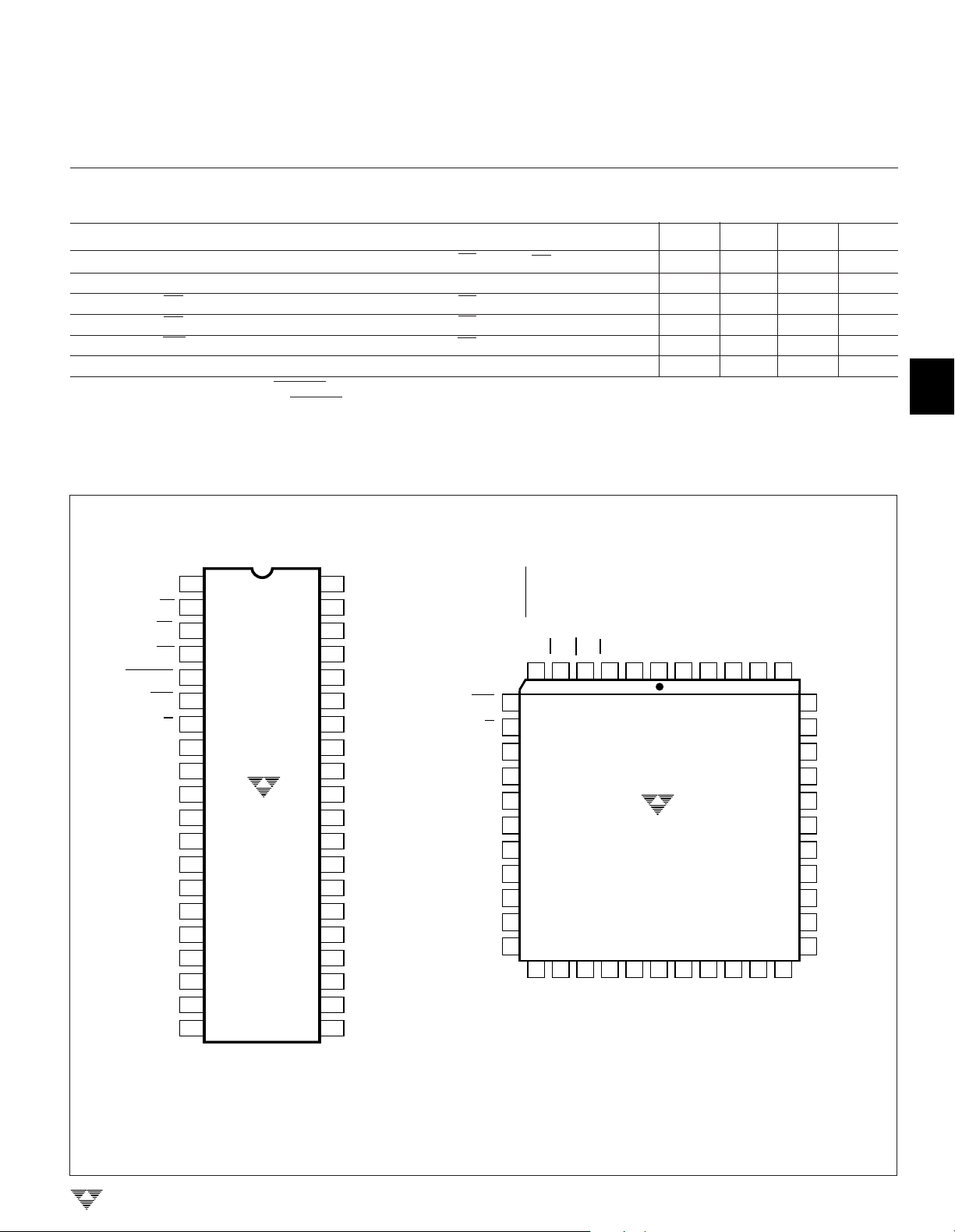
■ 40-Pin Dual-in-Line or 44-Pin PLCC Packages
FUNCTIONAL BLOCK DIAGRAM
C
R
INT
–
+
÷4
5
CONT/
DEMAND
BUF
25363439
BUFFER
INT
INT IN
TC850
7
L/H6OVR/
POL
INT OUT
–
+
INTEGRATOR
BUS INTERFACE
DECODE LOGIC
3
4RD1CS2
WR
2324
CE
22
COMPARATOR
+
–
6-BIT
UP/DOWN
COUNTER
DATA LATCH
OCTAL 2-INPUT MUX
3-STATE DATA BUS
. . . .
15
DB0
COMMON
+
REF
2
+
1
ANALOG
MUX
CONTROL
SEQUENCER
1
–
REF
A/D
18
OSC
2
REF
32
+
IN
31
–
IN
30
CLOCK
OSCILLATOR
17
OSC
+5V–5V
40
9-BIT
UP/DOWN
COUNTER
8
DB7
P-P
GENERAL DESCRIPTION
The TC850 is a monolithic CMOS analog-to-digital
converter (ADC) with resolution of 15-bits plus sign. It
combines a chopper-stabilized buffer and integrator with a
unique multiple-slope integration technique that increases
conversion speed. The result is 16 times improvement in
speed over previous 15-bit, monolithic integrating ADCs
(from 2.5 conversions per sec up to 40 per sec). Faster
conversion speed is especially welcome in systems with
human interface, such as digital scales.
The TC850 incorporates an ADC and a µP-compatible
digital interface. Only a voltage reference and a few noncritical passive components are required to form a complete 15bit plus sign ADC.
CMOS processing provides the TC850 with highimpedance differential inputs. Input bias current is typically
only 30pA, permitting direct interface to sensors. Input
sensitivity of 100µV per least significant bit (LSB) eliminates
the need for precision external amplifiers. The internal
amplifiers are auto-zeroed, guaranteeing a zero digital output
with 0V analog input. Zero adjustment potentiometers or
calibrations are not required.
The TC850 outputs data on an 8-bit, 3-state bus. Digital
inputs are CMOS compatible; outputs are TTL/CMOS compatible. Chip-enable and byte-select inputs combined with
an end-of-conversion output ensures easy interfacing to a
wide variety of microprocessors. Conversions can be performed continuously or on command. In continuous mode,
data is read as three consecutive bytes and manipulation of
address lines is not required.
Operating from ±5V supplies, the TC850 dissipates only
20mW. It is packaged in 40-pin plastic or ceramic dual-inline packages (DIPs) and in a 44-pin plastic leaded chip
carrier (PLCC), surface-mount package.
ORDERING INFORMATION
Part No. Package Temperature Range
TC850CLW 44-Pin PLCC 0°C to +70°C
TC850CPL 40-Pin Plastic DIP 0°C to +70°C
TC850IJL 40-Pin CerDIP – 25°C to +85°C
TC850ILW 44-Pin PLCC – 25°C to +85°C
3
4
5
6
7
TELCOM SEMICONDUCTOR, INC.
8
TC850-4 11/5/96
3-77

TC850
15-BIT, FAST-INTEGRATING CMOS
ANALOG-TO-DIGITAL CONVERTER
ABSOLUTE MAXIMUM RATINGS*
Positive Supply Voltage (VDD to GND)....................... +6V
Negative Supply Voltage (VSS to GND) .....................– 9V
Analog Input voltage (IN+ or IN–) .....................VDD to V
Voltage Reference Input
Logic Input Voltage ................ V
Current Into Any Pin.................................................10mA
Ambient Operating Temperature Range
ELECTRICAL CHARACTERISTICS: V
(REF
+
1
, REF
–
, REF
1
+
)..............................VDD to V
2
+ 0.3V to GND – 0.3V
DD
While Operating................................................100µA
C Device ................................................0°C to +70°C
I Device.............................................– 25°C to +85°C
= ±5V, f
S
Lead Temperature (Soldering, 10 sec) .................+300°C
Package Power Dissipation (TA ≤ 70°C)
CerDIP..............................................................2.29W
Plastic DIP ........................................................1.23W
SS
SS
CLK
Plastic PLCC ....................................................1.23W
*Static-sensitive device. Unused devices must be stored in conductive
material. Protect devices from static discharge and static fields. Stresses
above those listed under Absolute Maximum Ratings may cause permanent damage to the device. These are stress ratings only and functional
operation of the device at these or any other conditions above those
indicated in the operational sections of the specifications is not implied.
Exposure to Absolute Maximum Rating Conditions for extended periods
may affect device reliability.
= 61.44 kHz, VFS = 3.2768V, TA = 25°C, Fig. 1 Test Circuit,
unless otherwise specified.
Symbol Parameter Test Conditions Min Typ Max Unit
Zero-Scale Error VIN = 0V ±0.25 ±0.5 LSB
End Point Linearity Error –VFS ≤ VIN ≤ +V
FS
Differential Nonlinearity — ±0.1 ±0.5 LSB
I
IN
Input Leakage Current VIN = 0V, TA = 25°C — 30 75 pA
0°C ≤ T
≤ +70°C ———
A
– 25° ≤ TA ≤ +85°C — 1.1 3 nA
V
CMR
Common-Mode Voltage Range Over Operating Temperature Range VSS + 1.5 — VDD – 1.5 V
CMRR Common-Mode Rejection Ratio VIN = 0V, VCM = ±1V — 80 — dB
Full-Scale Gain Temperature External Ref Temperature
Coefficient Coefficient = 0 ppm/°C — 2 5 ppm/°C
0°C ≤ TA ≤ +70°C
Zero-Scale Error V
= 0V — 0.3 2 µV/°C
IN
Temperature Coefficient 0°C ≤ TA ≤ +70°C
Full-Scale Magnitude V
= ±3.275V — 0.5 2 LSB
IN
Symmetry Error
e
I
S
I
S
V
V
I
OP
V
IL
I
PU
I
PD
I
OSC
C
C
t
CE
t
RE
t
DHC
t
DHR
t
OP
N
+
–
OH
OL
IH
IN
OUT
Input Noise Not Exceeded 95% of Time — 30 — µV
Positive Supply Current — 2 3.5 mA
Negative Supply Current — 2 3.5 mA
Output High Voltage IO = 500 µA 3.5 4.9 — V
Output Low Voltage IO = 1.6 mA — 0.15 0.4 V
Output Leakage Current Pins 8 – 15, High-Impedance State — 0.1 1 µA
Input High Voltage Note 3 3.5 2.3 — V
Input Low Voltage Note 3 — 2.1 1 V
Input Pull-Up Current Pins 2, 3, 4, 6, 7; VIN = 0V — 4 — µA
Input Pull-Down Current Pins 1, 5; VIN = 5V — 14 — µA
Oscillator Output Current Pin 18, V
= 2.5V — 140 — µA
OUT
Input Capacitance Pins 1 – 7, 17 — 1 — pF
Output Capacitance Pins 8 – 15, High-Impedance State — 15 — pF
Chip-Enable Access Time CS or CE, RD = LOW (Note 1) — 230 450 nsec
Read-Enable Access Time CS = HIGH, CE = LOW (Note 1) — 190 450 nsec
Data Hold From CS or CE RD = LOW (Note 1) — 250 450 nsec
Data Hold From RD CS = HIGH, CE = LOW (Note 1) — 210 450 nsec
OVR/POL Data Access Time CS = HIGH, CE = LOW, RD = LOW (Note 1) — 140 300 nsec
— ±1 ±2 LSB
P-P
3-78
TELCOM SEMICONDUCTOR, INC.
15-BIT, FAST-INTEGRATING CMOS
ANALOG-TO-DIGITAL CONVERTER
ELECTRICAL CHARACTERISTICS (Cont.)
1
TC850
Symbol Parameter Test Conditions Min Typ Max Unit
t
LH
t
WRE
t
WRD
t
WWR
NOTES: 1. Demand mode, CONT/DEMAND = LOW. Figure 10 timing diagram. CL = 100pF.
Low/High Byte Access Time CS = HIGH, CE = LOW, RD = LOW (Note 1) — 140 300 nsec
Clock Setup Time Positive or Negative Pulse Width 100 — — nsec
RD Minimum Pulse Width CS = HIGH, CE = LOW (Note 2) 450 230 — nsec
RD Minimum Delay Time CS = HIGH, CE = LOW (Note 2) 150 50 — nsec
WR Minimum Pulse Width CS = HIGH, CE = LOW, Demand Mode 75 25 — nsec
Clock Setup Time Positive or Negative Pulse Width 100 — — nsec
2. Continuous mode, CONT/DEMAND = HIGH. Figure 12 timing diagram.
3. Digital inputs have CMOS logic levels and internal pull-up/pull-down resistors. For TTL compatibility, external pull-up resistors to VCC are
recommended.
PIN CONFIGURATIONS
CS
CE
WR
RD
CONT/DEMAND
OVR/POL
L/H
DB7
DB6
DB5
DB4
DB3
DB2
DB1
DB0
BUSY
OSC
OSC
TEST
GND
1
2
3
4
5
6
7
8
9
10
TC850CPL
11
TC850IJL
12
13
14
15
16
17
1
18
2
19
20
40
39
38
37
36
35
34
33
32
31
30
29
28
27
26
25
24
23
22
21
V
DD
+
REF
1
+
C
REF1
–
C
REF1
–
REF
–
C
REF2
+
C
REF2
+
REF
2
+
IN
–
IN
COMMON
C
INTB
C
INTA
C
BUFA
C
BUFB
BUFFER
INT
IN
INT
OUT
V
SS
COMP
OVR/POL
L/H
DB7
DB6
DB5
NC
DB4
DB3
DB2
DB1
DB0
CONT/DEMAND
RD
6543 1442
7
8
9
10
11
12
13
18 19 20 21 23 24
OSC
BUSY
CE
WR
TC850CLW
TC850ILW
1
2
TEST
OSC
22
CS
GND
NC
NC
DD
V
COMP
1
+
43 42 41 40
25 26 27 28
REF
SS
V
+
REF1
C
OUT
INT
–
REF1
C
IN
INT
–
REF
39
38
37
36
35
34
33
3214
3115
3016
2917
BUFFER
–
C
REF2
+
C
REF2
+
REF
2
+
IN
–
IN
NC
COMMON
C
INTB
C
INTA
C
BUFA
C
BUFB
2
3
4
5
6
7
TELCOM SEMICONDUCTOR, INC.
NC = NO INTERNAL CONNECTION
8
3-79

15-BIT, FAST-INTEGRATING CMOS
ANALOG-TO-DIGITAL CONVERTER
TC850
PIN DESCRIPTIONS
40-Pin DIP
Pin No. Symbol Description
1 CS Chip select, active HIGH. Logically ANDed with CE to enable read and write inputs. (See
2 CE Chip enable, active LOW. (See note 5.)
3 WR Write input, active LOW. When chip is selected (CS = HIGH and CE = LOW) and in demand
4 RD Read input, active LOW. When CS = HIGH and CE = LOW, a logic LOW on RD enables the
5 CONT/DEMAND Conversion control input. When CONT/DEMAND = LOW, conversions are initiated by the WR
6 OVR/POL Overrange/polarity data-select input. When making conversions in the demand mode (CONT/
7 L/H Low/high byte-select input. When CONT/DEMAND = LOW, this input controls whether low-
8 DB7 Most significant data bit output. When reading the A/D conversion result, the polarity,
9 – 15 DB6–DB0 Data outputs DB6–DB0. 3-state, bus compatible.
16 BUSY A/D conversion status output. BUSY goes to a logic HIGH at the beginning of the deintegrate
17 OSC
18 OSC
1
2
19 TEST For factory testing purposes only. Do not make external connection to this pin.
20 DGND Digital ground connection.
21 COMP Connection for comparator auto-zero capacitor. Bypass to VSS with 0.1 µF.
22 V
23 INT
24 INT
SS
OUT
IN
25 BUFFER Output of the input buffer. Connect to R
26 C
27 C
28 C
29 C
BUFB
BUFA
INTA
INTB
30 COMMON Analog common.
31 IN
–
30 COMMON Analog common.
REF2
REF2
REF1
REF1
DD
+
2
+
–
–
–
+
+
1
33 REF
34 C
35 C
36 REF
37 C
38 C
39 REF
40 V
NOTES: 4. This pin incorporates a pull-down resistor to DGND.
5. This pin incorporates a pull-up resistor to VDD.
note 4.)
mode (CONT/DEMAND = LOW), a logic LOW on WR starts a conversion. (See note 4.)
3-state data outputs. (See note 5.)
input. When CONT/DEMAND = HIGH, conversions are performed continuously. (See note 4.)
DEMAND = LOW), OVR/POL controls the data output on DB7 when the high-order byte is
active. (See note 5.)
byte or high-byte data is enabled on DB0 through DB7. (See note 5.)
overrange, and DB7 data are output on this pin. (See text.)
phase and goes LOW when conversion is complete. The falling edge of BUSY can be used to
generate a µP interrupt.
Crystal oscillator connection or external oscillator input.
Crystal oscillator connection.
Negative power supply connection, typically – 5V.
Output of the integrator amplifier. Connect to C
Input to the integrator amplifier. Connect to summing node of R
INT
.
INT
INT
and C
INT
.
.
Connection for buffer auto-zero capacitor. Bypass to VSS with 0.1 µF.
Connection to buffer auto-zero capacitor. Bypass to VSS with 0.1 µF.
Connection for integrator auto-zero capacitor. Bypass to VSS with 0.1 µF.
Connection for integrator auto-zero capacitor. Bypass to VSS with 0.1 µF.
Negative differential analog input.
Positive input for reference voltage V
Positive connection for V
Negative connection for V
reference capacitor.
REF2
reference capacitor.
REF2
REF2
. (V
REF2
= V
REF1
/64)
Negative input for reference voltages.
Negative connection for V
Positive connection for V
Positive input for V
REF1
reference capacitor.
REF1
reference capacitor.
REF1
.
Positive power supply connection, typically +5V.
3-80
TELCOM SEMICONDUCTOR, INC.
15-BIT, FAST-INTEGRATING CMOS
ANALOG-TO-DIGITAL CONVERTER
1
TC850
THEORY OF OPERATION
The TC850 is a multiple-slope, integrating analog-todigital converter (ADC). The multiple-slope conversion process, combined with chopper-stabilized amplifiers, results
in a significant increase in ADC speed, while maintaining
very high resolution and accuracy.
Dual-Slope Conversion Principles
The conventional dual-slope converter measurement
cycle (shown in Figure 2A) has two distinct phases:
(1) Input signal integration
(2) Reference voltage integration (deintegration)
The input signal being converted is integrated for a fixed
time period, measured by counting clock pulses. An opposite polarity constant reference voltage is then integrated
until the integrator output voltage returns to zero. The
reference integration time is directly proportional to the input
signal.
In a simple dual-slope converter, complete conversion
requires the integrator output to "ramp-up" and "rampdown." Most dual-slope converters add a third phase, autozero. During auto-zero, offset voltages of the input buffer,
integrator, and comparator are nulled, thereby eliminating
the need for zero-offset adjustments.
Dual-slope converter accuracy is unrelated to the integrating resistor and capacitor values, as long as they are
stable during a measurement cycle. By converting the
unknown analog input voltage into an easily-measured
function of time, the dual-slope converter reduces the need
for expensive, precision passive components.
Noise immunity is an inherent benefit of the integrating
conversion method. Noise spikes are integrated, or averaged, to zero during the integration period. Integrating ADCs
are immune to the large conversion errors that plague
successive approximation converters in high-noise environments.
A simple mathematical equation relates the input signal,
reference voltage, and integration time:
t
SI
1
RC
VIN(t) dt = ,
∫
0
where: VR = Reference voltage
tSI = Signal integration time (fixed)
tRI = Reference voltage integration time (variable).
VR t
RC
RI
Multiple-Slope Conversion Principles
One limitation of the dual-slope measurement technique is conversion speed. In a typical dual-slope method,
the auto-zero and integrate times are each one-half of the
deintegrate time. For a 15-bit conversion, 214+214+2
(65,536) clock pulses are required for auto-zero, integrate,
and deintegrate phases, respectively. The large number of
clock cycles effectively limits the conversion rate to about
2.5 conversions per second, when a typical analog CMOS
fabrication process is used.
The TC850 uses a multiple-slope conversion technique
to increase conversion speed (Figure 2B). This technique
makes use of a two-slope deintegration phase and permits
15-bit resolution up to 40 conversions per second.
During the TC850's deintegration phase, the integration
capacitor is rapidly discharged to yield a resolution of 9 bits.
At this point, some charge will remain on the capacitor. This
remaining charge is then slowly deintegrated, producing an
2240
V
SS
COMMON
C
C
C
C
BUFFER
INT
C
BUFACBUFB
0.1
µF
–5V
REF
REF
REF
+
REF1
–
REF1
+
REF2
–
REF2
INT
OUT
TEST
IN
26
IN
100 MΩ
32
+
0.1
µF
31
30
39
33
36
38
37
34
35
25
24
23
19
0.01 µF INPUT
+1.6384V
+0.0265V
1 µF
1 µF
120 MΩ
R
INT
0.1µF
C
INT
NC
–
+
1
+
2
–
IN
+5V
20
V
DGND
DD
16
BUSY
8
DB7
9
DB6
10
DB5
11
DB4
12
DB3
13
DB2
14
DB1
15
DB0
1
CS
2
CE
3
WR
4
RD
5
CONT/DEMAND
6
OVR/POL
7
L/H
17
**
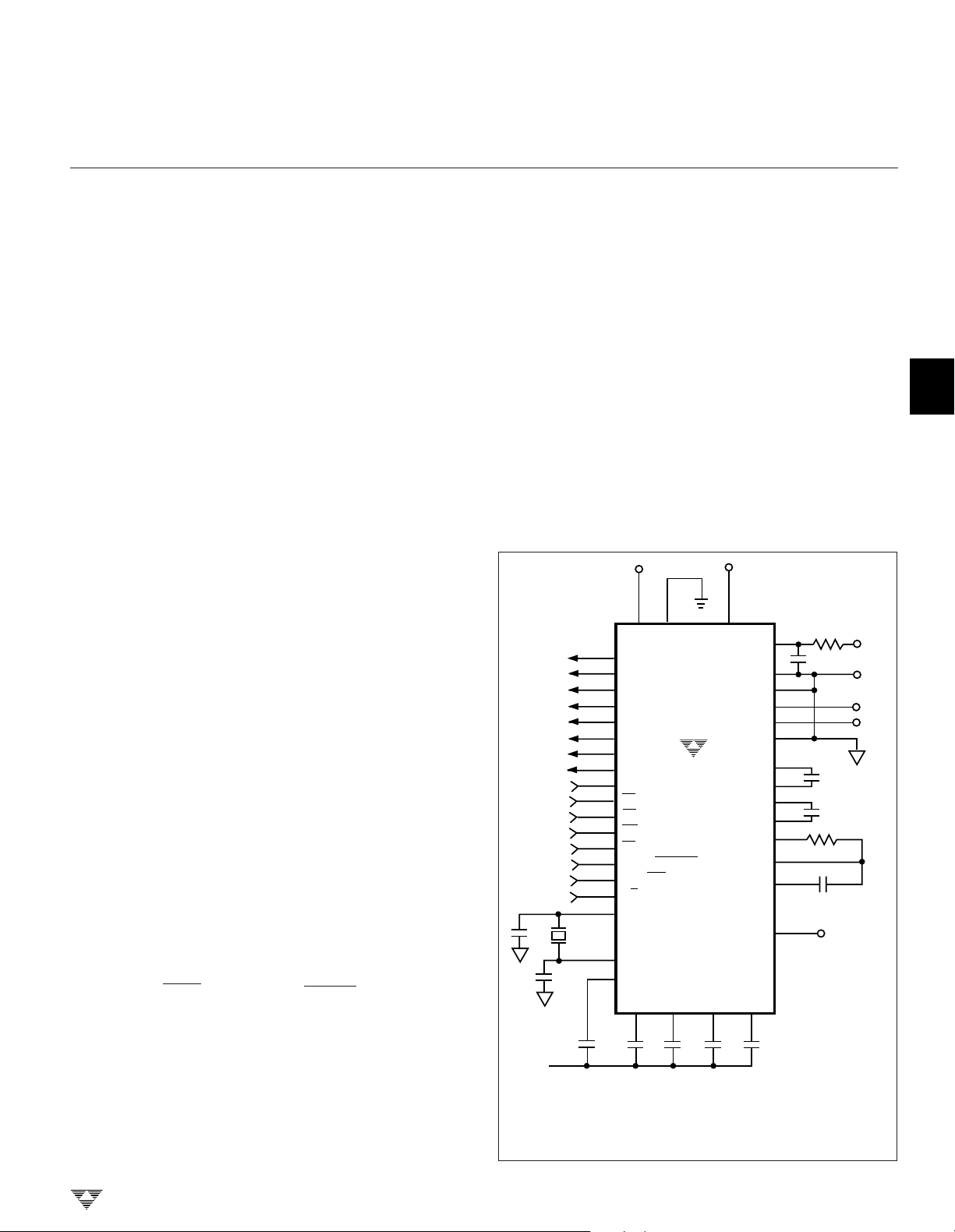
NOTES: Unless otherwise specified, all 0.1µF capacitors are film dielectric.
61.44 kHz
**
Ceramic capacitors are not recommended.
NC = No internal capacitors
*Polypropylene capacitors.
** 100pF Mica capacitors.
OSC
18
OSC
21
COMP
C
INTA
0.1
µF
Figure 1. Standard Circuit Configuration
1
2
C
INTB
28 2729
0.1
µF
TC850
0.1
µF
15
*
*
2
3
4
5
6
7
8
TELCOM SEMICONDUCTOR, INC.
3-81
 Loading...