

TelCom Semiconductor Inc TC820CPL, TC820CLW, TC820CKW Datasheet
3-3/4 DIGIT A/D CONVERTER WITH FREQUENCY
COUNTER AND LOGIC PROBE
FEATURES
■ Multiple Analog Measurement System
— Digit A/D Converter
— Frequency Counter
— Logic Probe
■ Low Noise A/D Converter:
— Differential Inputs, (1pA Bias Current)
— On-Chip 50PPM/°C Voltage Reference
■ Frequency Counter:
— 4Mhz Maximum Input Frequency
— Auto-ranging Over Four Decade Range
■ Logic Probe:
— Two LCD Annunciators
— Buzzer Driver
■ 3-3/4 Digit Display with Overrange Indicator
■ LCD Display Driver with Built-in Contrast Control
■ Data Hold Input for Comparison Measurements
■ Low Battery Detect with LCD Annunciator
■ Underrange and Overrange Outputs
■ On-Chip Buzzer Driver with Control Input
■ 44-Pin Plastic Flat Pack or PLCC or 40-Pin Plastic
DIP Packages
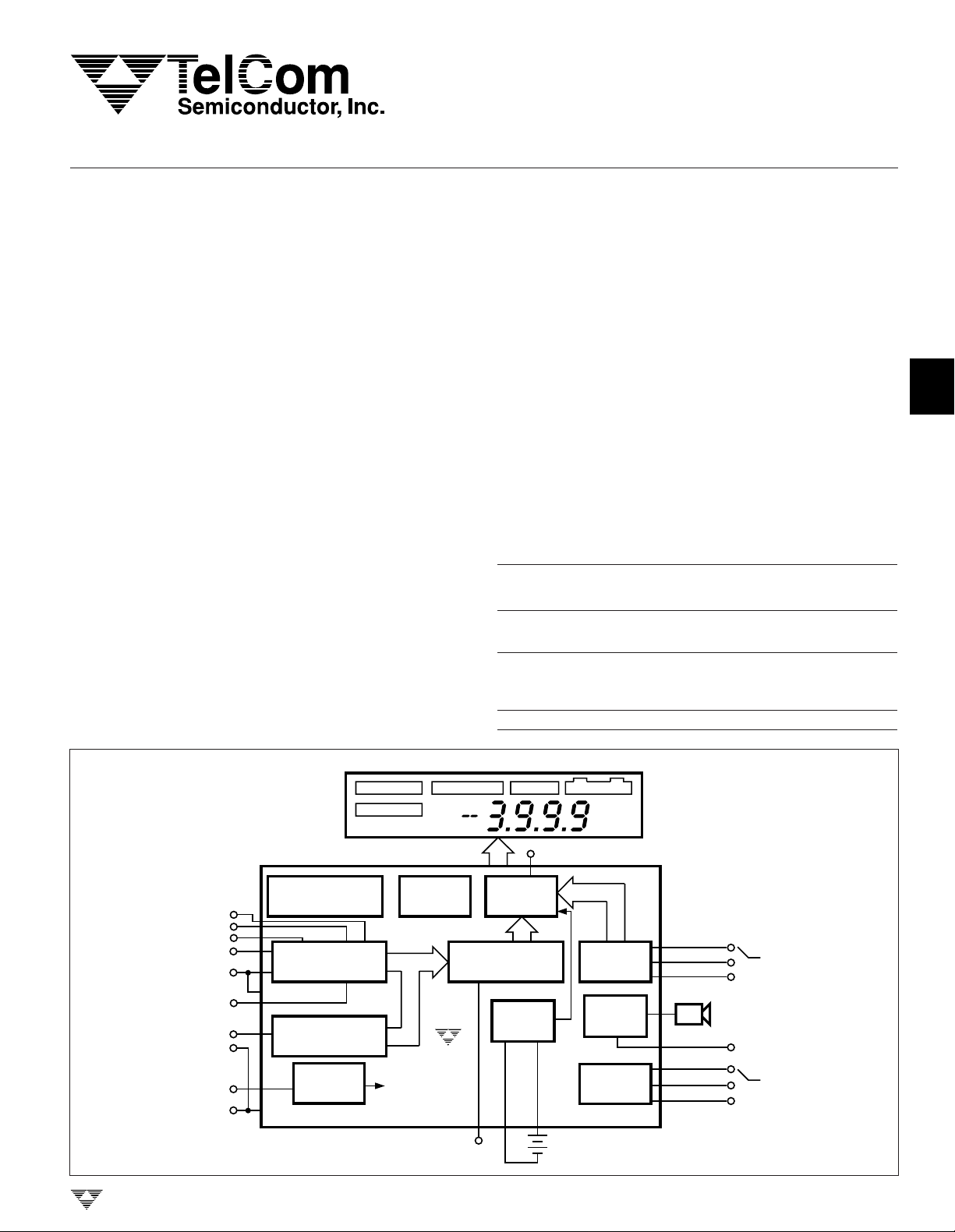
FUNCTIONAL BLOCK DIAGRAM
LOGIC HIGH
LOGIC LOW
OVERRANGE PKHOLD LOW BATT
GENERAL DESCRIPTION
The TC820 is a 3-3/4 digit, multi-measurement system
especially suited for use in portable instruments. It integrates a dual slope A/D converter, auto-ranging frequency
counter and logic probe into a single 44-pin surface mount
or 40-pin through hole package. The TC820 operates from
a single 9V input voltage (battery) and features a built-in
battery low flag. Function and decimal point selection are
accomplished with simple logic inputs designed for direct
connection to an external microcontroller or rotary switch.
Ease of use, low power operation and high functional
integration make the TC820 desirable in a variety of analog
measurement applications.
ORDERING INFORMATION
Part No. Resolution Package Range
TC820CKW 3-3/4 Digits 44-Pin Plastic 0°C to +70°C
TC820CLW 3-3/4 Digits 44-Pin Plastic 0°C to +70°C
TC820CPL 3-3/4 Digits 40-Pin Plastic DIP 0°C to +70°C
TRIPLEX LCD
Quad Flat Package
Leadless Chip
Carrier
1
TC820
2
3
4
Temperature
5
LOW DRIFT VOLTAGE
DIFFERENTIAL
UNDERRANGE
EOC
OVERRANGE
ANALOG
INPUT
FULL-SCALE
SELECT
FREQUENCY
INPUT
LOGIC
PROBE
INPUT
REFERENCE
3-3/4 DIGIT
A/D CONVERTER
ANALOG GND
AUTORANGING
FREQUENCY
COUNTER
LOGIC
PROBE
DIGITAL GROUND
TELCOM SEMICONDUCTOR, INC.
CLOCK
OSCILLATOR
TC820
TO LCD
AND BUZZER
TRIPLE LCD
DRIVERS
PEAK HOLD
COMPARATOR
LOW
BATTERY
DETECT
PEAK
HOLD
ANNUNCIATOR DRIVE
DECIMAL
DRIVERS
BUZZER
FUNCTION
SELECT
+
9V
POINT
DRIVER
VOLTS
FREQUENCY
LOGIC
DECIMAL
POINT
SELECT
BUZZER
CONTROL
FUNCTION
SELECT
6
7
8
TC820-10 10/17/96
3-149

TC820
3-3/4 DIGIT A/D CONVERTER WITH
FREQUENCY AND LOGIC PROBE
GENERAL DESCRIPTION
The TC820 is a 3-3/4 digit measurement system combining an integrating analog-to-digital converter, frequency
counter, and logic level tester in a single package. The
TC820 supersedes the TC7106 in new designs by improving performance and reducing system cost. The TC820
adds features that are difficult, expensive, or impossible to
provide with older A/D converters (see the competitive
evaluation). The high level of integration permits TC820based instruments to deliver higher performance and more
features, while actually reducing parts count. Fabricated in
low-power CMOS, the TC820 directly drives a 3-3/4 digit
(3999 maximum) LCD.
With a maximum range of 3999 counts, the TC820
provides 10 times greater resolution in the 200mV to 400mV
range than traditional 3-1/2 digit meters. An auto-zero cycle
guarantees a zero reading with a 0V input. CMOS processing reduces analog input bias current to only 1pA. Rollover
error (the difference in readings for equal magnitude but
opposite polarity input signals) is less than ±1 count. Differential reference inputs permit ratiometric measurements for
ohms or bridge transducer applications.
The TC820's frequency counter option simplifies design
of an instrument well-suited to both analog and digital
troubleshooting: voltage, current, and resistance measurements, plus precise frequency measurements to 4MHz
(higher frequencies can be measured with an external
prescaler), and a simple logic probe. The frequency counter
will automatically adjust its range to match the input frequency, over a four-decade range.
Two logic level measurement inputs permit a TC820based meter to function as a logic probe. When combined
with external level shifters, the TC820 will display logic levels
on the LCD and also turn on a piezoelectric buzzer when the
measured logic level is low.
Other TC820 features simplify instrument design and
reduce parts count. On-chip decimal point drivers are included, as is a low battery detection annunciator. A piezoelectric buzzer can be controlled with an external switch or
by the logic probe inputs. Two oscillator options are provided: A crystal can be used if high accuracy frequency
measurements are desired, or a simple RC option can be
used for low-end instruments.
A "peak reading hold" input allows the TC820 to retain
the highest A/D or frequency reading. This feature is useful
in measuring motor starting current, maximum temperature, and similar applications.
A family of instruments can be created with the TC820.
No additional design effort is required to create instruments
with 3-3/4 digit resolution.
The TC820 operates from a single 9V battery, with
typical power of 10 mW. Packages include a 40-pin plastic
DIP, 44-pin plastic flat package, and 44-pin PLCC.
COMPETITIVE EVALUATION
Features Comparison TC820 7106
3-3/4 Digit Resolution Yes No
Auto-Ranging Frequency Counter Yes No
Logic Probe Yes No
Decimal Point Drive Yes No
Peak Reading Hold Yes No
(Frequency or Voltage)
Display Hold Yes No
Simple 10:1 Range Change Yes No
Buzzer Drive Yes No
Low Battery Detection Yes No
With Annunciator
Overrange Detection Yes No
With Annunciator
Low Drift Reference Yes No
Underrange/Overrange Yes No
Logic Output
Input Overload Display "OL" "1"
LCD Annunciator Driver Yes No
LCD Drive Type Triplexed Direct
LCD Pin Connections 15 24
LCD Elements 36 23
3-150
TELCOM SEMICONDUCTOR, INC.
3-3/4 DIGIT A/D CONVERTER WITH
FREQUENCY AND LOGIC PROBE
1
TC820
ABSOLUTE MAXIMUM RATINGS*
Supply Voltage (VDD to GND) .....................................15V
Analog Input Voltage (Either Input) (Note 1) ....VDD to V
Reference Input Voltage (Either Input).............VDD to V
Digital Inputs ............................................... VDD to DGND
V
............................................. VDD to (DGND – 0.3V)
DISP
Package Power Dissipation (TA ≤ 70°C) (Note 2)
40-Pin Plastic DIP.............................................1.23W
44-Pin PLCC.....................................................1.23W
44-Pin Plastic Flat Package..............................1.00W
Operating Temperature Range
"C" Devices............................................ 0°C to +70°C
"E" Devices .......................................– 40°C to +85°C
Storage Temperature Range ................– 65°C to +150°C
Lead Temperature (Soldering, 10 sec) ................... 300°C
ELECTRICAL CHARACTERISTICS: V
Symbol Parameter Test Conditions Min Typ Max Units
Zero Input Reading VIN = 0V – 000 ±000 +000 Digital
RE Roll-Over Error VIN = ±390mV – 1 ±0.2 +1 Counts
NL Nonlinearity (Maximum Full-Scale = 400mV – 1 ±0.2 +1 Count
CMRR Common-Mode Rejection V
VCMR Common-Mode Voltage Input High, Input Low V
e
N
I
IN
V
COM
V
CTC
TC
ZS
TC
FS
I
S
Deviation From Best
Straight Line Fit)
Ratiometric Reading VIN = V
Ratio Full-Scale = 400mV
Range
Noise (P-P Value Not VIN = 0V — 15 — µV
Exceeded 95% of Time) Full-Scale = 400mV
Input Leakage Current VIN = 0V
Analog Common Voltage 25 kΩ Between Common and V
Common Voltage 25 kΩ Between Common and V
Temperature Coefficient 0°C ≤ TA ≤ +70°C — 35 50 ppm/°C
Zero Reading Drift VIN = 0V
Scale Factor VIN = 399mV
Temperature Coefficient 0°C ≤ T
Supply Current VIN = 0V — 1 1.5 mA
Peak-to-Peak Backplane V
Drive Voltage V
Full Scale = 400 mV Reading
Full-Scale = 400mV
(VFS = 200 mV)
T
0°C ≤ T
– 40°C ≤ TA ≤ +85°C — 100 —
(VSS – V
– 40°C ≤ TA ≤ +85°C—50—
0°C ≤ T
– 40°C ≤ TA ≤ +85°C1
– 40°C ≤ TA ≤ +85°C—5—
Ext Ref = 0 ppm/°C
= 9V, TA = 25°C, unless otherwise specified.
S
, TC820 1999 1999/2000 2000 Digital
REF
= ±1V, VIN = 0V — 50 — µV/V
CM
= 25°C—110pA
A
≤ +70°C—20—
A
) 3.15 3.3 3.45 V
COM
≤ +70°C — 0.2 — µV/°C
A
≤ +70°C — 1 5 ppm/°C
A
= 9V 4.25 4.7 5.3 V
S
= DGND
DISP
*Static-sensitive devices. Unused devices should be stored in conductive
material to protect against static discharge and static fields. Stresses above
those listed under Absolute Maximum Ratings may cause permanent
damage to the device. These are stress ratings only, and functional
SS
operation of the device at these or any other conditions above those
SS
indicated in the operational sections of the specifications is not implied.
Exposure to absolute maximum rating conditions for extended periods may
affect device reliability.
NOTES: 1. Input voltages may exceed the supply voltages provided that
input current is limited to ±100µA. Current above this value
may result in invalid display readings but will not destroy the
device if limited to ±1mA.
2. Dissipation ratings assume device is mounted with all leads
soldered to printed circuit board.
+ 1.5 — VDD– 1 V
SS
DD
DD
2
3
4
5
6
7
8
TELCOM SEMICONDUCTOR, INC.
3-151
3-3/4 A/D CONVERTER WITH
FREQUENCY COUNTER
AND LOGIC PROBE
TC820
ELECTRICAL CHARACTERISTICS (Cont.)
Symbol Parameter Test Conditions Min Typ Max Units
Buzzer Frequency f
Counter Timebase Period f
Low Battery Flag Voltage V
V
IL
V
IH
V
OL
Input Low Voltage — — DGND + 1.5 V
Input High Voltage V
Output Low Voltage, IL = 50µA — — DGND + 0.4 V
UR, OR Outputs
V
OL
Output High Voltage, IL = 50µAV
UR, OR Outputs
Control Pin VIN = V
Pull-Down Current
PIN DESCRIPTION
= 40kHz — 5 — kHz
OSC
= 40kHz — 1 — Second
OSC
DD
to V
SS
DD
6.7 7 7.3 V
– 1.5 — — V
DD
– 1.5 — — V
DD
—5 —µA
Pin No. Pin No.
(40-Pin (44-Pin Flat
Package) Package) Symbol Description
1 40 L-E4 LCD segment driver for L ("logic LOW"), polarity, and "e" segment of most
significant digit (MSD).
2 41 AGD4 LCD segment drive for "a," "g," and "d" segments of MSD.
3 42 BC4P3 LCD segment drive for "b" and "c" segments of MSD and decimal point 3.
4 43 HFE3 LCD segment drive for H ("logic HIGH"), and "f" and "e" segments of third LSD.
5 44 AGD3 LCD segment drive for "a," "g," and "d" segments of third LSD.
6 1 BC3P2 LCD segment drive for "b" and "c" segments of third LSD and decimal point 2.
7 2 OFE2 LCD segment drive for "overrange," and "f" and "e" segments of second LSD.
8 3 AGD2 LCD segment drive for "a," "g," and "d" segments of second LSD.
9 4 BC2P1 LCD segment drive for "b " and "c" segments of second LSD and decimal point 1.
10 5 PKFE1 LCD segment drive for "hold peak reading," and "f" and "e" segments of LSD.
11 6 AGD1 LCD segment drive for "a," "g," and "d" segments of LSD.
12 7 BC1BT LCD segment drive for "b" and "c" segments of LSD and "low battery."
13 8 BP3 LCD backplane #3.
14 9 BP2 LCD backplane #2.
15 10 BP1 LCD backplane #1.
—11V
DISP
16 12 DGND Internal logic digital ground, the logic "0" level. Nominally 4.7V below VDD.
17 13 ANNUNC Square-wave output at the backplane frequency, synchronized to BP1. ANNUNC
18 14 LOGIC Logic mode control input. When connected to V
19 15 RANGE/ Dual-purpose input. In range mode, when connected to VDD, the integration time
FREQ will be 200 counts instead of 2000 counts and the LCD will display the analog input
Sets peak LCD drive signal: V
PEAK
= (V
DD
) –V
DISP
. V
may also be used to
DISP
compensate for temperature variation of LCD crystal threshold voltage.
can be used to control display annunciators. Connecting an LCD segment to
ANNUNC turns it on; connecting it to its backplane turns it off.
, the converter is in logic mode.
DD
The LCD displays "OL" and the decimal point inputs control the HIGH and LOW
annunciators. When the "low" annunciator is on, the buzzer will also be on. When
unconnected or connected to DGND, the TC820 is in the voltage/frequency
measurement mode. This pin has a 5µA internal pull-down to DGND.
divided by 10. (See text for limitation withTC820.) In frequency mode, this pin is the
frequency input. A digital signal applied to this pin will be measured with a 1-second
time base. There is an internal 5µA pull-down to DGND.
3-152
TELCOM SEMICONDUCTOR, INC.

3-3/4 A/D CONVERTER WITH
FREQUENCY COUNTER
AND LOGIC PROBE
PIN DESCRIPTION
1
TC820
Pin No. Pin No.
(40-Pin (44-Pin Flat
Package) Package) Symbol Description
20 16 DP0/LO Dual-purpose input. Decimal point select input for voltage measurements. In logic
mode, connecting this pin to VDD will turn on the "low" LCD segment. There is an
internal 5µA pull-down to DGND in volts mode only. Decimal point logic:
DP1 DP0 Decimal Point Selected
0 0 None
0 1 DP1
1 0 DP2
1 1 DP3
21 17 DP1/HI Dual-purpose input. Decimal point select input for voltage measurements. In logic
mode, connecting this pin to V
internal 5µA pull-down to DGND in volts mode only.
22 18 BUZOUT Buzzer output. Audio frequency, 5kHz, output which drives a piezoelectric buzzer.
23 19 BUZIN Buzzer control input. Connecting BUZIN to V
logically ORed (internally) with the "logic level low" input. There is an internal 5µA
pull-down to DGND.
24 20 FREQ/ Voltage or frequency measurement select input. When unconnected, or connected
VOLTS to DGND, the A/D converter function is active. When connected to V
frequency counter function is active. This pin has an internal 5µA pull-down
to DGND.
25 21 PKHOLD Peak hold input. When connected to V
if a new conversion value is greater than the preceding value. Thus, the peak
reading will be stored and held indefinitely. When unconnected, or connected to
DGND, the converter will operate normally. This pin has an internal 5µA pull-down
to DGND.
22 UR Underrange output. This output will be HIGH when the digital reading is 380 counts
or less.
23 OR Overrange output. This output will be HIGH when the analog signal input is greater
than full scale. The LCD will display "OL" when the input is overranged.
26 24 V
27 25 COM Analog circuit ground reference point. Nominally 3.3V below VDD.
28 26 C
29 27 C
30 28 V
31 29 V
32 30 V
33 31 V
34 32 V
35 33 C
36 34 V
35 EOC/ Bidirectional pin. Pulses low (i.e., from V
37 36 OSC1 Crystal oscillator (input) connection.
38 37 OSC2 Crystal oscillator (output) connection.
39 38 OSC3 RC oscillator connection.
40 39 V
SS
+
REF
–
REF
+
REF
–
REF
–
IN
+
IN
BUFF
AZ
INT
HOLD conversion. If connected to VDD, conversions will continue, but the display is not
DD
Negative supply connection. Connect to negative terminal of 9V battery.
Positive connection for reference capacitor.
Negative connection for reference capacitor.
High differential reference input connection.
Low differential reference input connection.
Low analog input signal connection.
High analog input signal connection.
Buffer output. Connect to integration resistor.
Auto-zero capacitor connection.
Integrator output. Connect to integration capacitor.
updated.
Positive power supply connection, typically 9V.
will turn on the "high" LCD segment. There is an
DD
turns the buzzer on. BUZIN is
DD
, the
DD
, the converter will only update the display
DD
to DGND) at the end of each
DD
2
3
4
5
6
7
8
TELCOM SEMICONDUCTOR, INC.
3-153

TC820
PIN CONFIGURATIONS
3-3/4 A/D CONVERTER WITH
FREQUENCY COUNTER
AND LOGIC PROBE
SEGMENTS L-E4
SEGMENTS AGD4
SEGMENTS BC4P3
SEGMENTS HFE3
SEGMENTS AGD3
SEGMENTS BC3P2
SEGMENTS OFE2
SEGMENTS AGD2
SEGMENTS BCP1
SEGMENTS PKFE1
SEGMENTS AGD1
SEGMENTS BC1BT
BP3
BP2
BP1
DGND
ANNUNC
LOGIC
RANGE/FREQ
DP0/LO
1
2
3
4
5
6
7
8
9
10
11
12
13
14
15
16
17
18
19
20
TC820CPL
V
40
OSC3
39
38
OSC2
OSC1
37
V
36
C
35
V
34
V
33
V
32
V
31
V
30
C
29
28
C
COM
27
V
26
25
PK HOLD
24
FREQ/VOLTS
23
BUZ IN
22
BUZ OUT
21
DP1/HI
DD
INT
AZ
BUFF
+
IN
–
IN
–
REF
+
REF
–
REF
+
REF
SS
BC3P2
OFE2
AGD2
BC2P1
PKFE1
AGD1
BP1BT
BP3
BP2
BP1
V
DISP
BC3P2
OFE2
AGD2
BCP2P1
PKFE1
AGD1
BP1BT
BP3
BP2
BP1
V
DISP
AGD3
HFE3
BC4P3
6543 1442
7
8
9
10
11
12
13
18 19 20 21 23 24
DGND
AGD4
TC820CLW
LOGIC
ANNUNC
RANGE/FREQ
AGD3
BC4P3
HFE3
44 43 42 41 39 3840
1
2
3
4
5
6
7
8
9
10
11
12 13 14 15 17 18
AGD4
TC820CKW
L-E4
22
DP0/LO
L–E4
16
DD
V
DP1/HI
DD
V
OSC3
BUZ OUT
OSC3
OSC242OSC141EOC/HOLD
43
25 26 27 28
40
INT
V
UR
BUZ IN
PK HOLD
FREQ/VOLTS
INT
V
OSC1
OSC2
37 36 35
19 20 21 22
EOC/HOLD
34
39
38
37
36
35
34
33
3214
3115
3016
2917
33
32
31
30
29
28
27
26
25
24
23
C
AZ
V
BUFF
+
V
IN
–
V
IN
–
V
REF
+
V
REF
–
C
REF
+
C
REF
COM
V
SS
OR
C
AZ
V
BUFF
+
V
IN
–
V
IN
–
V
REF
+
V
REF
–
C
REF
+
C
REF
COM
V
SS
OR
3-154
DGND
LOGIC
ANNUNC
UR
DP1/HI
DP0/LO
RANGE/FREQ
BUZ IN
BUZ OUT
PK HOLD
FREQ/VOLTS
TELCOM SEMICONDUCTOR, INC.
3-3/4 A/D CONVERTER WITH
FREQUENCY COUNTER
AND LOGIC PROBE
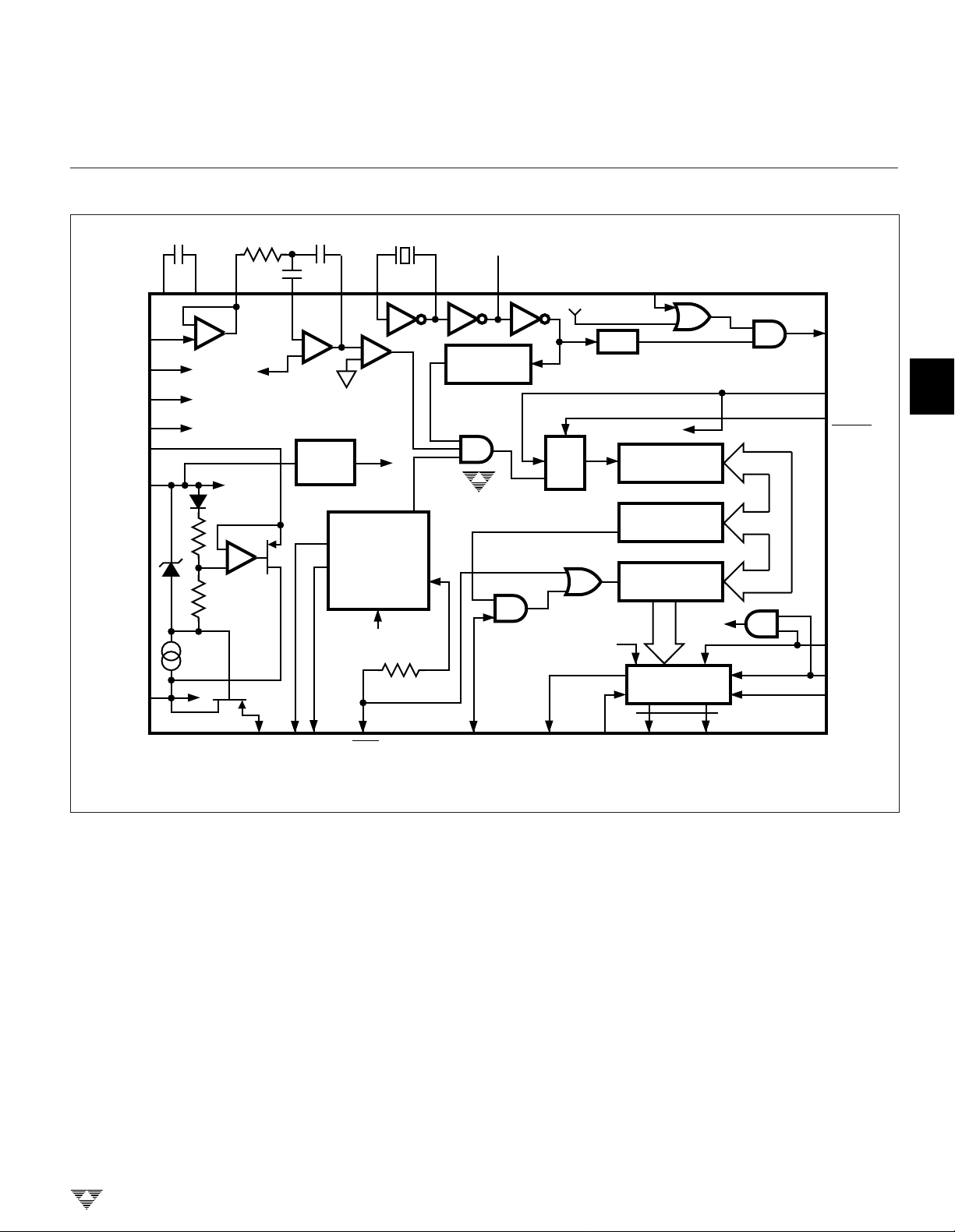
FUNCTIONAL BLOCK DIAGRAM
1
TC820
2
C
V
V
+
V
REF
–
V
REF
COMMON
V
DD
V
SS
+
REF
+
IN
–
IN
–
C
REFVBUFF
C
V
AZ
INT
LOW
BATT
DETECT
A/D CONTROL
UNDERRANGE
OVERRANGE
RANGE/FREQ
TO LCD
DEINT
RANGE
INPUT
EOC
÷2
TC820
OSC3OSC2OSC1
BUZ IN
LOGIC
LOW
÷8
FREQUENCY COUNTER INPUT
A/D COUNTER SELECT
RANGE
SEL
B
A
LOW BATT
A/D COUNTER
(3999 COUNTS)
COMPARATOR
A > B
DISPLAY
LATCH
LOGIC
TRIPLEX
DRIVERS
LOW
15
BUZZER
DRIVER
RANGE/
FREQ
FREQ/
VOLTS
LOGIC
DP0/LO
DP1/HI
3
4
5
DGND
UR OR
EOC/
HOLD
PEAK
HOLD
ANNUNC
V
DISP
SEG0 • • • BP3
6
7
8
TELCOM SEMICONDUCTOR, INC.
3-155
 Loading...