

TelCom Semiconductor Inc TC811CPL, TC811CKW Datasheet
3-1/2 DIGIT A/D CONVERTER WITH HOLD AND DIFFERENTIAL
REFERENCE INPUTS
1
TC811
2
FEATURES
■ Differential Reference Input
■ Display Hold Function
■ Fast Over-Range Recovery, Guaranteed Next
Reading Accuracy
■ Low Temperature Drift Internal
Reference ....................................... 35ppm/°C (Typ)
■ Guaranteed Zero Reading With Zero Input
■ Low Noise..................................................... 15µV
■ High Resolution (0.05%) and Wide Dynamic
Range (72 dB)
■ High Impedance Differential Input
■ Low Input Leakage Current .......................1pA Typ
10pA Max
■ Direct LCD Drive – No External Components
■ Precision Null Detection with True Polarity at Zero
■ Crystal Clock Oscillator
■ Available in DIP, Compact Flat Package or PLCC
■ Convenient 9V Battery Operation with
Low Power Dissipation (600µA Typical, 1mW
Maximum)
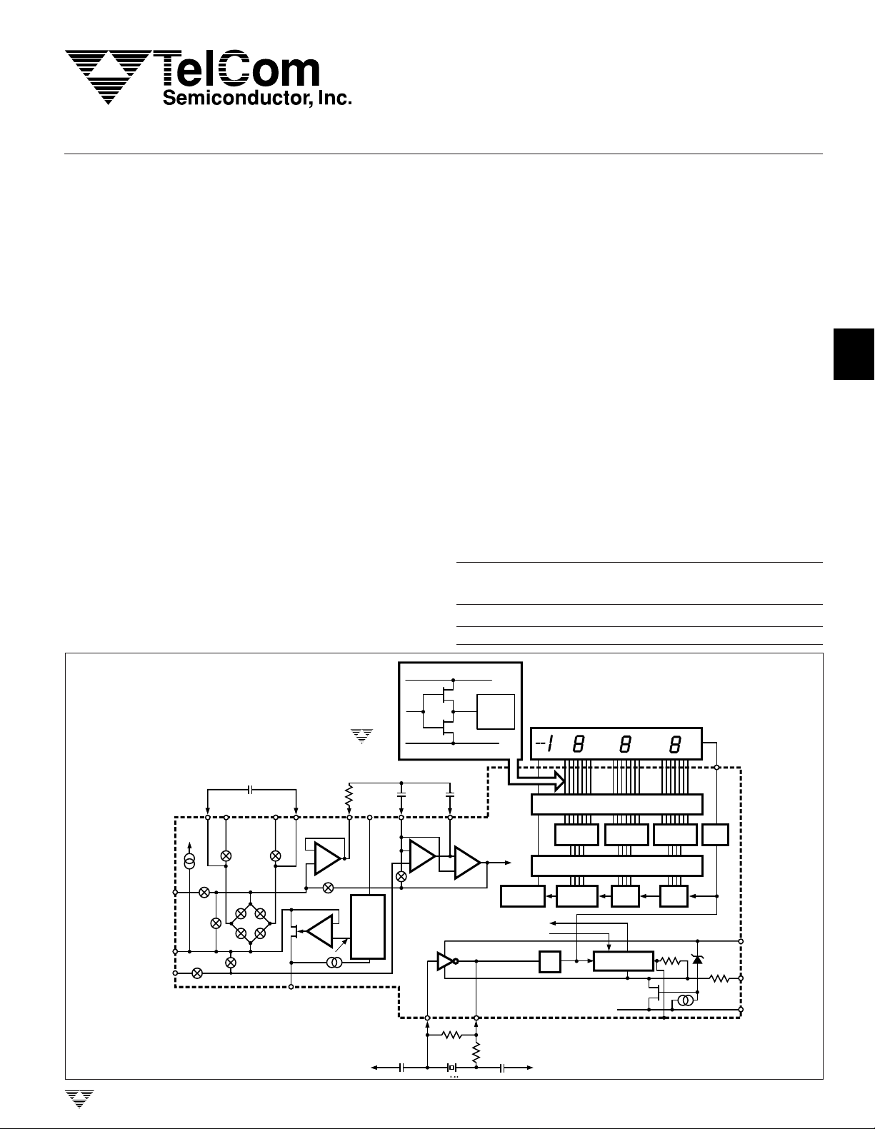
FUNCTIONAL BLOCK DIAGRAM
p-p
TYPICAL APPLICATIONS
■ Thermometry
■ Digital Meters
— Voltage/Current/Power
— pH Measurement
— Capacitance/Inductance
— Fluid Flow Rate/Viscosity
— Humidity
— Position
■ Panel Meters
■ LVDT Indicators
■ Portable Instrumentation
■ Digital Scales
■ Process Monitors
■ Gaussometers
■ Photometers
ORDERING INFORMATION
Temp. Max V
Part No. Package Range Tempco
TC811CKW 44-PQFP 0°C to +70°C 75 ppm/°C
TC811CPL
40-Pin Plastic DIP
0°C to +70°C 75 ppm/°C
REF
3
4
5
C
REF
V
ANALOG
COMMON
V
+
+
V
C
REF
REF
10
µA
31
+
IN
INT
A/Z
32
30
–
IN
DE (+)
INT
ZI & A/Z
DE
(–)DE(+)
AZ & DE (±)
V
DE (–)
–
REF
–
C
REF
33
ZI &
A/Z
V+– 3.0V
26
–
V
TELCOM SEMICONDUCTOR, INC.
V
BUFF
–
+
ZI
–
+
TC811CPL
R
INT
+
V
28
LOW
TEMPCO
V
REF
+
V
TYPICAL SEGMENT OUTPUT
INTERNAL DIGITAL GROUND
C
AZ
29
38
INTEGRATOR
–
+
A/Z
COMPARATOR
40
OSC
1
10pF
+
V
0.5mA
SEGMENT
OUTPUT
2mA
C
INT
V
INT
27343635
TO
DIGITAL
SECTION
+
–
THOUSANDS
TO SWITCH DRIVERS
FROM COMPARATOR OUTPUT
CLOCK
39
22MΩ
470k
OSC
2
20pF
f
OSC
LCD DISPLAY
LCD SEGMENT DRIVERS
7 SEGMENT
DECODE
HUNDREDS
4
INTERNAL DIGITAL GOUND
+
V
7 SEGMENT
DATA LATCH
CONTROL LOGIC
7 SEGMENT
V
= 1V
DECODE
≈70kΩ
TH
1
HLDR
DECODE
TENS UNITS
BACKPLANE
21
200
6.2V
Ω
500
38
V
TEST
26
V
6
7
+
–
8
TC811-7 11/5/96
3-137
TC811
3-1/2 DIGIT A/D CONVERTER WITH HOLD AND
DIFFERENTIAL REFERENCE INPUTS
GENERAL DESCRIPTION
The TC811 is a low power, 3-1/2 digit, LCD display
analog-to-digital converter. This device incorporates both a
display hold feature and differential reference inputs. A
crystal oscillator, which only requires two pins, permits
added features while retaining a 40-pin package. An additional feature is an "Integrator Output Zero" phase which
guarantees rapid input overrange recovery.
The TC811 display hold (HLDR) function can be used to
"freeze" the LCD display. The displayed reading will remain
indefinitely as long as HLDR is held high. Conversions
continue but the output data display latches are not updated.
The TC811 also includes a differential reference for easy
ratiometric measurements. Circuits which use the
7106/26/36 can easily be upgraded to include the hold
function with the TC811.
The TC811 has an improved internal zener reference
voltage circuit which maintains the Analog Common temperature drift to 35ppm/°C (typical) and 75ppm/°C (maximum). This represents an improvement of two to four times
over similar 3-1/2 digit converters, eliminating the need for
a costly, space consuming external reference source.
The TC811 limits linearity error to less than one count on
both the 200mV and the 2.00V full-scale ranges. Rollover
error—the difference in readings for equal magnitude but
opposite polarity input signals—is below ±1 count. High
impedance differential inputs offer 1pA leakage currents
and a 1012Ω input impedance. The 15µV
mance guarantees a “rock solid” reading. The Auto Zero
cycle guarantees a zero display readout for a zero volt input.
The single chip CMOS TC811 incorporates all the active
devices for a 3-1/2 digit analog to digital converter to directly
drive an LCD display. Onboard oscillator, precision voltage
reference and display segment and backplane drivers sim-
noise perfor-
p-p
plify system integration, reduce board space requirements
and lower total cost. A low cost, high resolution (0.05%)
indicating meter requires only a TC811, an LCD display, five
resistors, six capacitors, a crystal, and a 9V battery. Compact, hand held multimeter designs benefit from the TelCom
Semiconductor small footprint package option.
The TC811 uses a dual slope conversion technique
which will reject interference signals if the converters integration time is set to a multiple of the interference signal
period. This is especially useful in industrial measurement
environments where 50, 60 and 400Hz line frequency signals are present.
ABSOLUTE MAXIMUM RATINGS*
Supply Voltage (V+ to V–)............................................15V
Analog Input voltage (Either Input)1.....................V+ to V
Reference Input Voltage ...................................... V+ to V
Clock Input ......................................................TEST to V
Power Dissipation2 (TA ≤ 70°C)
44-Pin Flat Package .........................................1.00W
40-Pin Plastic DIP.............................................1.23W
Operating Temperature Range
Commercial Package (C) ......................0°C to +70°C
Industrial Package (I)........................– 25°C to +85°C
Storage Temperature Range ................– 65°C to +150°C
Lead Temperature (Soldering, 10 sec) .................+300°C
*Static-sensitive device. Unused devices must be stored in conductive
material. Protect devices from static discharge and static fields. Stresses
above those listed under "Absolute Maximum Ratings" may cause permanent damage to the device. These are stress ratings only and functional
operation of the device at these or any other conditions above those
indicated in the operation sections of the specifications is not implied.
Exposure to absolute maximum rating conditions for extended periods may
affect device reliability.
–
–
+
ELECTRICAL CHARACTERISTICS: V
Supply
= 9V, f
= 32.768kHz, and TA = 25°C, unless otherwise noted.
CLOCK
Symbol Parameter Test Conditions Min Typ Max Unit
Input
— Zero Input Reading VIN = 0V – 000.0 ±000.0 +000.0 Digital
VFS = 200mV Reading
— Zero Reading Drift VIN = 0V, 0°C ≤ TA ≤ 70°C — 0.2 1 µV/°C
— Ratiometric Reading VIN = V
NL Linearity Error VFS = 200mV or 2.000V – 1 ±0.2 +1 Counts
E
R
e
N
I
L
CMRR Common-Mode Rejection VCM = ±1V, VIN = 0V, — 50 — µV/V
3-138
Roll Over Error VIN– = VIN+ ≈ 200mV – 1 ±0.2 +1 Counts
Noise VIN = 0V, VFS = 200mV — 15 — µV
Input Leakage Current VIN = 0V — 1 10 pA
VFS = 200mV
REF
, V
= 100mV 999 999/1000 1000 Digital
REF
TELCOM SEMICONDUCTOR, INC.
Reading
P-P
3-1/2 DIGIT A/D CONVERTER WITH HOLD AND
DIFFERENTIAL REFERENCE INPUTS
1
TC811
ELECTRICAL CHARACTERISTICS: V
Supply
= 9V, f
= 32.768kHz, and TA = 25°C, unless otherwise noted.
CLOCK
Symbol Parameter Test Conditions Min Typ Max Unit
TC
SF
Analog Common Section
V
CTC
V
C
Hold Pin Input Section
V
IL
V
IH
LCD Drive Section
V
SD
V
SD
Power Supply
I
SUP
NOTES: 1. Input voltages may exceed supply voltages when input current is limited to 100µA.
Scale Factor Temperature VIN = 199mV, 0°C ≤ TA ≤ 70°C — 1 5 ppm/°C
Coefficient (ext. V
tc = 0ppm)
REF
Analog Common 250KΩ from V+ to Analog Common — — — —
Temperature Coefficient 0°C ≤ T
≤ 70°C————
A
"C" Commercial — 35 75 ppm/°C
"I" Industrial — 35 100 ppm/°C
Analog Common Voltage 250kΩ from V+ to Analog Common 2.7 3.05 3.35 Volts
Input Resistance Pin 1 to Pin 37 — 70 — kΩ
Input Low Voltage Pin 1 — — Test +1.5 V
Input High Voltage Pin 1 V+ – 1.5 — — V
3
LCD Segment Drive Voltage V+ to V– = 9V 4 5 6 V
LCD Backplane Drive Voltage V+ to V– = 9V 4 5 6 V
Power Supply Current VIN = 0V, V+ to V– = 9V — — — —
f
= 16kHz — 70 100 µA
OSC
f
= 48kHz — 90 125 µA
OSC
2. Dissipation rating assumes device is mounted with all leads soldered to a printed circuit board.
3. Backplane drive is in phase with the segment drive for "segment off" 180° out of phase for "segment on." Frequency is 20 times the
conversion rate. Average DC component is less than 50mV.
P-P
P-P
2
3
4
5
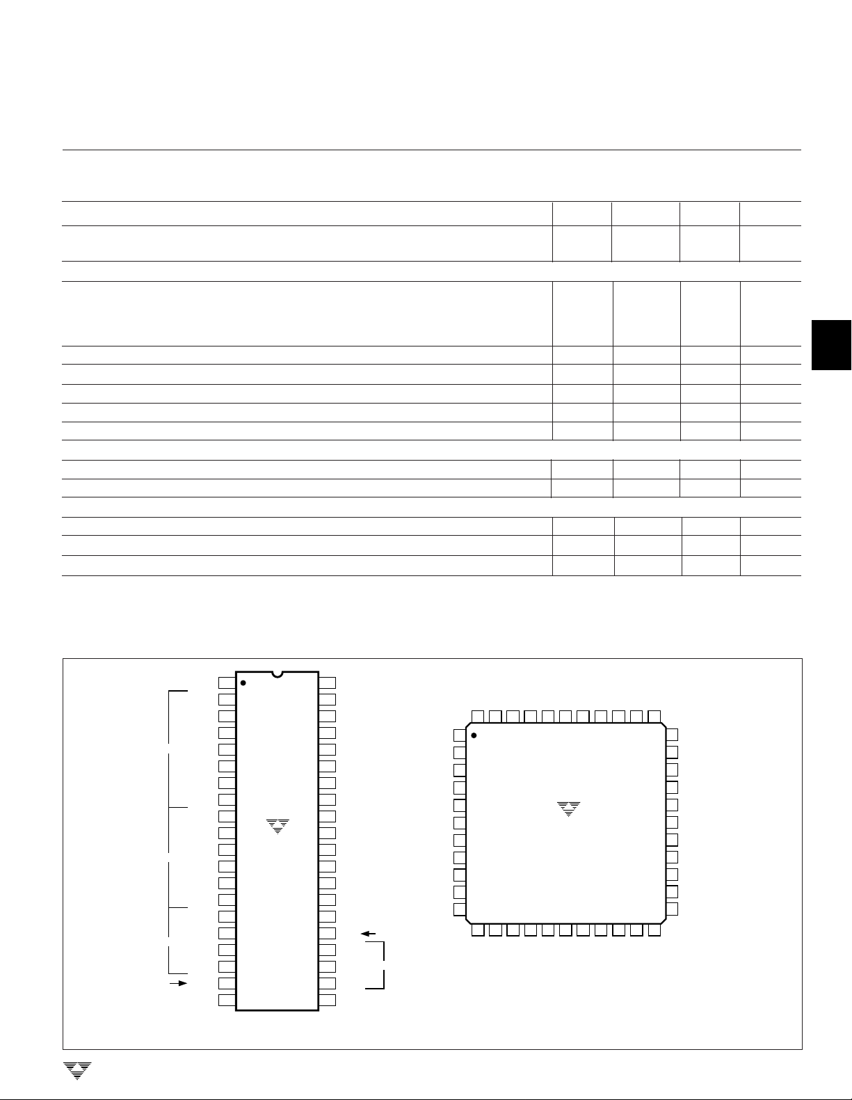
PIN CONFIGURATIONS
HLDR
D
C
B
1's
A
F
G
E
D
C
B
10's
A
F
E
D
B
100's
F
E
1000's
AB
POL
(MINUS SIGN)
28
OSC
40
OSC
39
38
37
36
35
34
33
32
31
30
29
27
26
25
24
23
22
21
1
NORMAL PIN
2
CONFIGURATION
1
3
1
4
1
5
1
6
1
7
1
8
1
9
2
10
2
2
2
2
2
3
3
3
3
4
NC = NO INTERNAL CONNECTION
11
12
13
14
15
16
17
18
19
20
TC811CPL
(40-PIN PDIP)
1
2
+
V
TEST
+
V
REF
+
C
REF
–
C
REF
–
V
REF
ANALOG
COMMON
+
V
IN
–
V
IN
C
AZ
V
BUFF
V
INT
–
V
G
10's
2
C
3
100's
A
3
G
3
BP
(BACKPLANE)
NC
NC
TEST
V
NC
OSC
OSC
HLDR
D
C
B
–
+
+
REF
REF
REF
C
C
V
44 43 42 41 39 3840
1
2
3
+
4
5
6
2
7
1
8
9
1
10
1
11
1
12 13 14 15 17 18
1F1G1E1
A
–
REF
COM
V
TC811CKW
(PQFP)
16
D2C2B2A
+
–
IN
V
BUFF35INT
IN
AZ
C
V
37
36
19 20 21 22
2F2E2
–
VVV
34
33
NC
32
G
2
C
31
3
30
A
3
29
G
3
BP
28
POL
27
26
AB
4
E
25
3
F
24
3
23
B
3
3
D
6
7
8
TELCOM SEMICONDUCTOR, INC.
3-139

3-1/2 DIGIT A/D CONVERTER WITH HOLD AND
DIFFERENTIAL REFERENCE INPUTS
TC811
PIN DESCRIPTION
Pin No.
40-Pin Plastic DIP Symbol Description
1 HLDR Hold pin, logic 1 holds present display reading.
2D
3C
4B
5A
6F
7G
8E
9D
10 C
11 B
12 A
13 F
14 E
15 D
16 B
17 F
18 E
19 AB
1
1
1
1
1
1
1
2
2
2
2
2
2
3
3
3
3
4
20 POL Activates the negative polarity display.
21 BP Backplane drive output.
22 G
23 A
24 C
25 G
26 V
27 V
28 V
29 C
3
3
3
2
–
INT
BUFF
AZ
30 VIN– Analog input low.
31 VIN+ Analog input high.
32 COM Analog Common: Internal zero reference.
33 V
34 C
35 C
36 V
– Reference input low.
REF
– Negative connection for reference capacitor.
REF
+ Positive connection for reference capacitor.
REF
+ Reference input high.
REF
37 TEST All LCD segment test when pulled high (V+).
38 V
39 OSC
40 OSC
+
2
1
Activates the D section of the units display.
Activates the C section of the units display.
Activates the B section of the units display.
Activates the A section of the units display.
Activates the F section of the units display.
Activates the G section of the units display.
Activates the E section of the units display.
Activates the D section of the tens display.
Activates the C section of the tens display.
Activates the B section of the tens display.
Activates the A section of the tens display.
Activates the F section of the tens display.
Activates the E section of the tens display.
Activates the D section of the hundreds display.
Activates the B section of the hundreds display.
Activates the F section of the hundreds display.
Activates the E section of the hundreds display.
Activates both halves of the 1 in the thousands display.
Activates the G section of the hundreds display.
Activates the A section of the hundreds display.
Activates the C section of the hundreds display.
Activates the G section of the tens display.
Negative power supply voltage.
Integrator output, connection for C
Buffer output, connection for R
Integrator input, connection for CAZ.
Positive power supply voltage.
Crystal oscillator output.
Crystal oscillator input.
INT
.
INT
.
3-140
TELCOM SEMICONDUCTOR, INC.
 Loading...