

TelCom Semiconductor Inc TC7662AMJA, TC7662AIJA, TC7662AEPA, TC7662ACPA Datasheet
CHARGE PUMP DC-TO-DC CONVERTER
EVALUATION
KIT
AVAILABLE
1
TC7662A
FEATURES
■ Wide Operating Range .............................3V to 18V
■ Increased Output Current .............................. 40mA
■ Pin Compatible with ICL7662/SI7661/TC7660/
LTC1044
■ No External Diodes Required
■ Low Output Impedance @ IL = 20mA....... 40Ω Typ.
■ No Low-Voltage Terminal Required
■ CMOS Construction
ORDERING INFORMATION
Temperature
Part No. Package Range
TC7662ACPA 8-Pin Plastic DIP 0°C to +70°C
TC7662AEPA 8-Pin Plastic DIP – 40°C to +85°C
TC7662AIJA 8-Pin CerDIP – 25°C to +85°C
TC7662AMJA 8-Pin CerDIP – 55°C to +125°C
TC7660EV Evaluation Kit for
Charge Pump Family
GENERAL DESCRIPTION
The TC7662A is a pin-compatible upgrade to the Industry standard TC7660 charge pump voltage converter. It
converts a +3V to +18V input to a corresponding – 3V to
-18V output using only two low-cost capacitors, eliminating
inductors and their associated cost, size and EMI. In addition to a wider power supply input range (3V to 18V versus
1.5V to 10V for the TC7660), the TC7662A can source
output currents as high as 40mA. The on-board oscillator
operates at a nominal frequency of 12kHz. Operation below 10kHz (for lower supply current applications) is also
possible by connecting an external capacitor from OSC to
ground.
The TC7662A directly is recommended for designs
requiring greater output current and/or lower input/output
voltage drop. It is available in 8-pin DIP packages in commercial and extended temperature ranges.
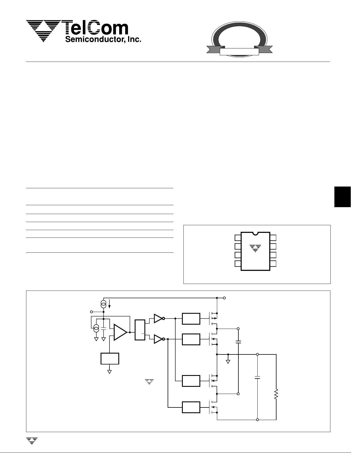
PIN CONFIGURATION
NC
C
GND
C
+
–
1
2
3
TC7662A
4
8
V
DD
OSC
7
6
NC
5
V
OUT
2
3
4
5
FUNCTIONAL BLOCK DIAGRAM
C
OSC
TELCOM SEMICONDUCTOR, INC.
NC = NO INTERNAL CONNECTION
8
V
P SW1
N SW4
N SW2
N SW3
DD
6
2
+
CAP
+
C
P
EXT
GND
3
+
C
OUT
4
CAP
R
EXT
–
5
V
OUT
R
L
TC7662A-5 9/11/96
7
8
4-77
I
7
LEVEL
SHIFT
LEVEL
SHIFT
LEVEL
SHIFT
LEVEL
SHIFT
+
–
COMPARATOR
WITH HYSTERESIS
V
REF
F/F
C
Q
Q
TC7662A
TC7662A
CHARGE PUMP
DC-TO-DC CONVERTER
ABSOLUTE MAXIMUM RATINGS*
Supply Voltage VDD to GND .................................... +18V
Input Voltage (Any Pin) ........... (VDD + 0.3) to (VSS – 0.3)
Current Into Any Pin.................................................10mA
Operating Temperature Range
C Suffix..................................................0°C to +70°C
I Suffix .............................................. – 25°C to +85°C
E Suffix.............................................– 40°C to +85°C
M Suffix .......................................... – 55°C to +125°C
Power Dissipation (TA ≤ 70°C)
Plastic DIP......................................................730mW
CerDIP............................................................800mW
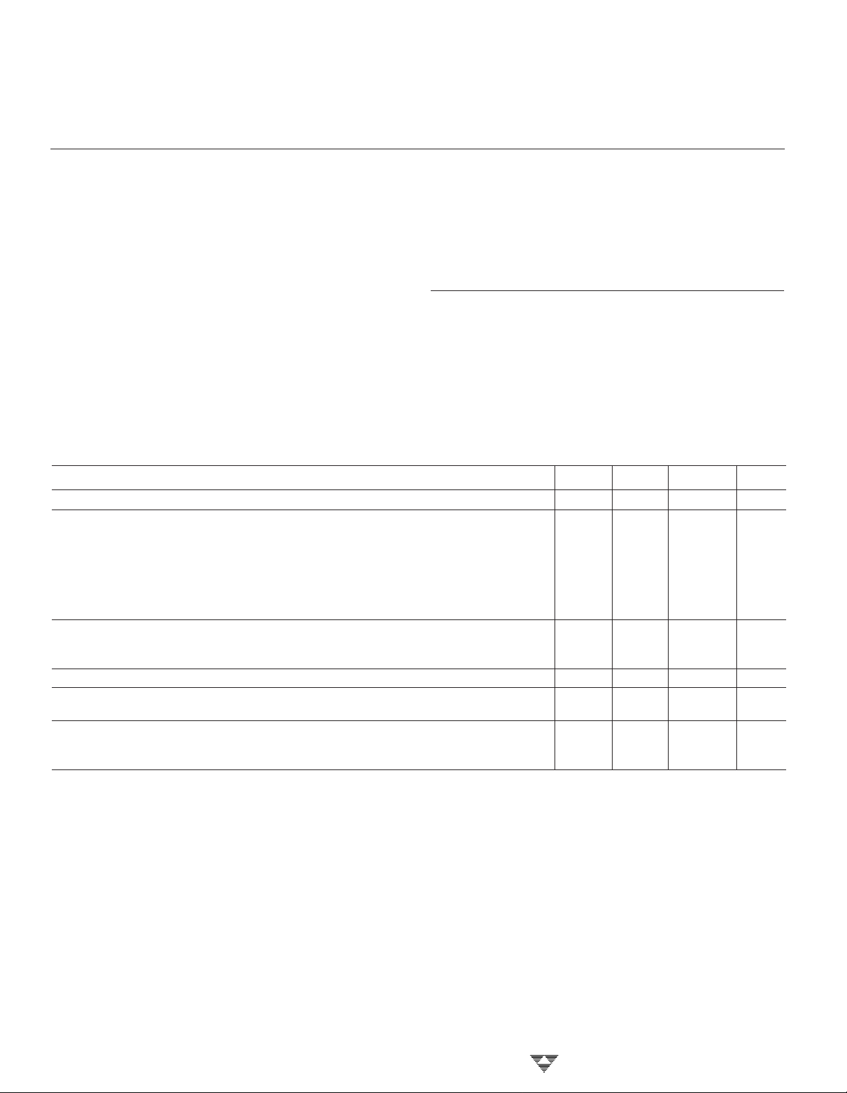
ELECTRICAL CHARACTERISTICS: V
= 15V, TA = +25°C (See Test Circuit), unless otherwise specified.
DD
Package Thermal Resistance
CPA, EPA θJA.............................................. 140°C/W
IJA, MJA θJA.................................................. 90°C/W
Storage Temperature Range ................– 65°C to +150°C
Lead Temperature (Soldering, 10 sec) .................+300°C
ESD Protection..................................................... ±2000V
Output Short Circuit................. Continuous (at 5.5V Input)
*Static-sensitive device. Unused devices must be stored in conductive
material. Protect devices from static discharge and static fields. Stresses
above those listed under Absolute Maximum Ratings may cause permanent damage to the device. These are stress ratings only and functional
operation of the device at these or any other conditions above those
indicated in the operational sections of the specifications is not implied.
Exposure to Absolute Maximum Rating Conditions for extended periods
may affect device reliability.
Symbol Parameter Test Conditions Min Typ Max Unit
V
I
R
C
P
V
DD
S
O
OSC
EFF
EFF
Supply Voltage 3 — 18 V
Supply Current RL = ∞
= +15V — 510 700 µA
V
DD
= +5V — 190 —
V
DD
Output Source IL = 20mA, VDD = +15V — 40 50 Ω
Resistance I
Oscillator Frequency — 12 — kHz
Power Efficiency VDD = +15V 93 97 — %
Voltage Efficiency VDD = +15V 99 99.9 — %
0°C ≤ T
– 55°C ≤ T
0°C ≤ T
– 55°C ≤ TA ≤ +125°C — 210 —
L
IL = 3mA, VDD = +5V — 100 125
RL = 2 kΩ
R
Over Operating Temperature Range 96 — —
≤ +70°C — 560 —
A
≤ +125°C — 650 —
A
≤ +70°C — 210 —
A
= 40mA, VDD = +15V — 50 60
= ∞
L
4-78
TELCOM SEMICONDUCTOR, INC.
 Loading...