

TelCom Semiconductor Inc TC7660SCOA, TC7660SMJA, TC7660SEPA, TC7660SEOA, TC7660SEJA Datasheet
...
SUPER CHARGE PUMP DC-TO-DC VOLTAGE CONVERTER
EVALUATION
KIT
AVAILABLE
FEATURES
GENERAL DESCRIPTION
1
TC7660S
2
■ Oscillator boost from 10kHz to 45kHz
■ Converts +5V Logic Supply to ±5V System
■ Wide Input Voltage Range ....................1.5V to 12V
■ Efficient Voltage Conversion.........................99.9%
■ Excellent Power Efficiency ...............................98%
■ Low Power Supply..............................80µA @ 5 V
■ Low Cost and Easy to Use
— Only Two External Capacitors Required
■ Available in Small Outline (SOIC) Package
■ Improved ESD Protection ..................... Up to 10kV
■ No External Diode Required for High Voltage
Operation
ORDERING INFORMATION
Temperature
Part No. Package Range
TC7660SCOA 8-Pin SOIC 0°C to +70°C
TC7660SCPA 8-Pin Plastic DIP 0°C to +70°C
TC7660SEJA 8-Pin CerDIP – 40°C to +85°C
TC7660SEOA 8-Pin SOIC – 40°C to +85°C
TC7660SEPA 8-Pin Plastic DIP – 40°C to +85°C
TC7660SMJA 8-Pin CerDIP – 55°C to +125°C
TC7660EV Evaluation Kit for
Charge Pump Family
The TC7660S is a pin-compatible upgrade to the Industry standard TC7660 charge pump voltage converter. It
converts a +1.5V to +12V input to a corresponding -1.5V to
-12V output using only two low-cost capacitors, eliminating
inductors and their associated cost, size and EMI. Added
features include an extended supply range to 12V, and a
IN
frequency boost pin for higher operating frequency, allowing
the use of smaller external capacitors.
The on-board oscillator operates at a nominal frequency
of 10kHz. Frequency is increased to 45kHz when pin 1 is
connected to V+. Operation below 10kHz (for lower supply
current applications) is possible by connecting an external
capacitor from OSC to ground (with pin 1 open).
The TC7660S is available in both 8-pin DIP and 8-pin
small outline (SOIC) packages in commercial and extended
temperature ranges.
PIN CONFIGURATION (DIP and SOIC)
Boost
CAP
GND
CAP
1
+
2
3
–
4
TC7660SCPA
TC7660SEJA
TC7660SEPA
+
8
V
7
OSC
LOW
6
VOLTAGE (LV)
5
V
OUT
Boost
CAP
GND
CAP
1
+
2
3
–
4
TC7660SCOA
TC7660SEOA
+
8
V
OSC
7
LOW
6
VOLTAGE (LV)
V
5
OUT
3
4
5
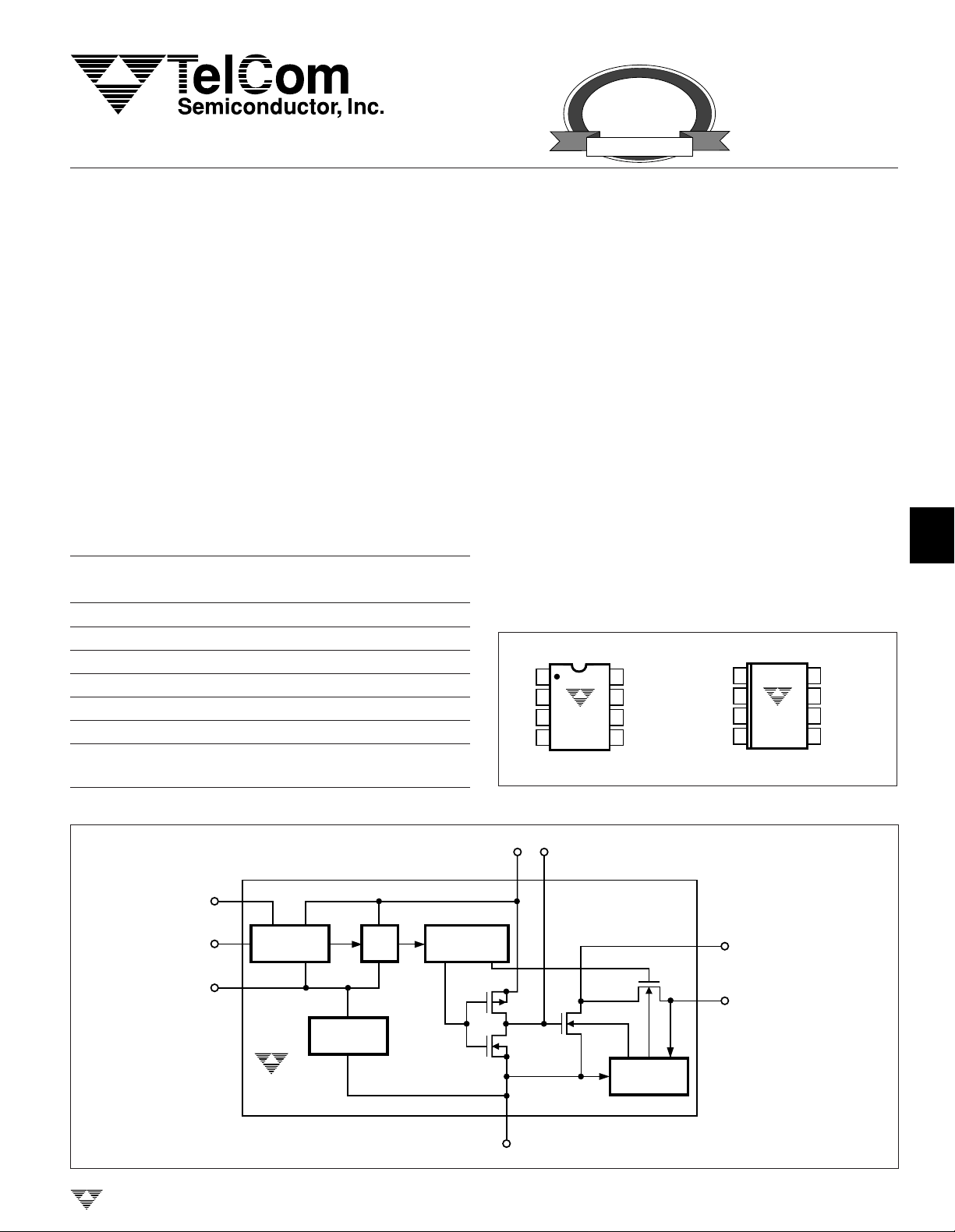
FUNCTIONAL BLOCK DIAGRAM
LV
1
7
6
BOOST
OSC
TELCOM SEMICONDUCTOR, INC.
RC
OSCILLATOR
TC7660S
INTERNAL
VOLTAGE
REGULATOR
÷ 2
VOLTAGE–
LEVEL
TRANSLATOR
V+CAP
82
3
GND
+
6
LOGIC
NETWORK
4
5
CAP
V
OUT
–
7
8
TC7660S-14 9/16/96
4-69
TC7660S
SUPER CHARGE PUMP DC-TO-DC
VOLTAGE CONVERTER
ABSOLUTE MAXIMUM RATINGS*
Supply Voltage ......................................................... +13V
LV, Boost, OSC Inputs
Voltage (Note 1) ......................... – 0.3V to (V+ +0.3V)
for V+ <5.5V
(V+ – 5.5V) to (V+ +0.3V)
for V+ >5.5V
Current Into LV (Note 1).......................20µA for V+ >3.5V
Output Short Duration (V
Power Dissipation (TA ≤ 70°C) (Note 2)
CerDIP............................................................800mW
Plastic DIP ......................................................730mW
SOIC...............................................................470mW
ELECTRICAL CHARACTERISTICS: T
≤ 5.5V) .........Continuous
SUPPLY
= +25°C, V+ = 5V, C
A
Operating Temperature Range
C Suffix ..................................................0°C to +70°C
E Suffix ............................................. – 40°C to +85°C
M Suffix........................................... – 55°C to +125°C
Storage Temperature Range ................– 65°C to +150°C
Lead Temperature (Soldering, 10 sec) .................+300°C
*Static-sensitive device. Unused devices must be stored in conductive
material. Protect devices from static discharge and static fields. Stresses
above those listed under "Absolute Maximum Ratings" may cause permanent damage to the device. These are stress ratings only and functional
operation of the device at these or any other conditions above those
indicated in the operation sections of the specifications is not implied.
Exposure to absolute maximum rating conditions for extended periods may
affect device reliability.
= 0, Test Circuit (Figure 1), unless otherwise
OSC
indicated.
Symbol Parameter Test Conditions Min Typ Max Unit
+
I
+
I
+
V
H
+
V
L
R
OUT
F
OSC
P
EFF
V
OUT EFF
Z
OSC
NOTES: 1. Connecting any input terminal to voltages greater than V+ or less than GND may cause destructive latch-up. It is recommended that no
Supply Current RL = ∞ — 80 160 µA
(Boost pin OPEN or GND) 0°C ≤ T
– 40°C ≤ T
≤ +70°C — — 180
A
≤ +85°C — — 180
A
– 55°C ≤ TA ≤ +125°C — — 200
Supply Current 0°C ≤ TA ≤ +70°C — — 300 µA
(Boost pin = V
+
) – 40°C ≤ TA ≤ +85°C — — 350
– 55°C ≤ TA ≤ +125°C — — 400
Supply Voltage Range, High Min ≤ TA ≤ Max, 3 — 12 V
RL = 10 kΩ, LV Open
Supply Voltage Range, Low Min ≤ TA ≤ Max, 1.5 — 3.5 V
RL = 10 kΩ, LV to GND
Output Source Resistance I
= 20mA — 60 100 Ω
OUT
I
= 20mA, 0°C ≤ TA ≤ +70°C — 70 120
OUT
I
= 20mA, – 40°C ≤ TA ≤ +85°C — 70 120
OUT
I
= 20mA, – 55°C ≤ TA ≤ +125°C — 105 150
OUT
V+ = 2V, I
0°C ≤ T
= 3 mA, LV to GND
OUT
≤ +70°C — — 250 Ω
A
– 55°C ≤ TA ≤ +125°C — — 400
Oscillator Frequency Pin 7 open; Pin 1 open or GND — 10 — kHz
Boost Pin = V
+
—45—
Power Efficiency RL = 5 kΩ; Boost Pin Open 96 98 — %
≤ TA ≤ T
T
MIN
Boost Pin = V
; Boost Pin Open 95 98 —
MAX
+
—88—
Voltage Conversion Efficiency RL = ∞ 99 99.9 — %
Oscillator Impedance V+ = 2V — 1 — MΩ
V+ = 5V — 100 — kΩ
inputs from sources operating from external supplies be applied prior to "power up" of the TC7660S.
2. Derate linearly above 50°C by 5.5mW/°C.
4-70
TELCOM SEMICONDUCTOR, INC.
SUPER CHARGE PUMP DC-TO-DC
V
+
GND
S
3
S
1
S
2
S
4
C
2
V
OUT
= – V
IN
C
1
VOLTAGE CONVERTER
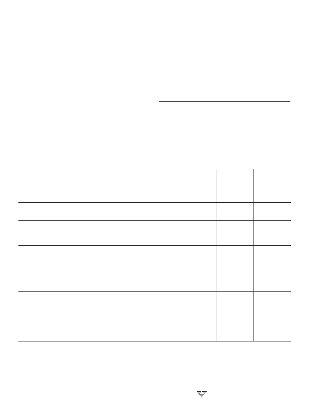
Detailed Description
1
TC7660S
The TC7660S contains all the necessary circuitry to
implement a voltage inverter, with the exception of two
external capacitors, which may be inexpensive 10 µF polarized electrolytic capacitors. Operation is best understood by
considering Figure 2, which shows an idealized voltage
inverter. Capacitor C1 is charged to a voltage V+ for the half
cycle when switches S1 and S3 are closed. (Note: Switches
S2 and S4 are open during this half cycle.) During the second
half cycle of operation, switches S2 and S4 are closed, with
S1 and S3 open, thereby shifting capacitor C1 negatively by
V+ volts. Charge is then transferred from C1 negatively by V+
volts. Charge is then transferred from C1 to C2, such that the
voltage on C2 is exactly V+, assuming ideal switches and no
load on C2.
The four switches in Figure 2 are MOS power switches;
S1 is a P-channel device, and S2, S3 and S4 are N-channel
devices. The main difficulty with this approach is that in
integrating the switches, the substrates of S3 and S4 must
always remain reverse-biased with respect to their sources,
but not so much as to degrade their ON resistances. In
addition, at circuit start-up, and under output short circuit
conditions (V
and the substrate bias adjusted accordingly. Failure to
accomplish this will result in high power losses and probable
device latch-up.
This problem is eliminated in the TC7660S by a logic
network which senses the output voltage (V
with the level translators, and switches the substrates of S
and S4 to the correct level to maintain necessary reverse
bias.
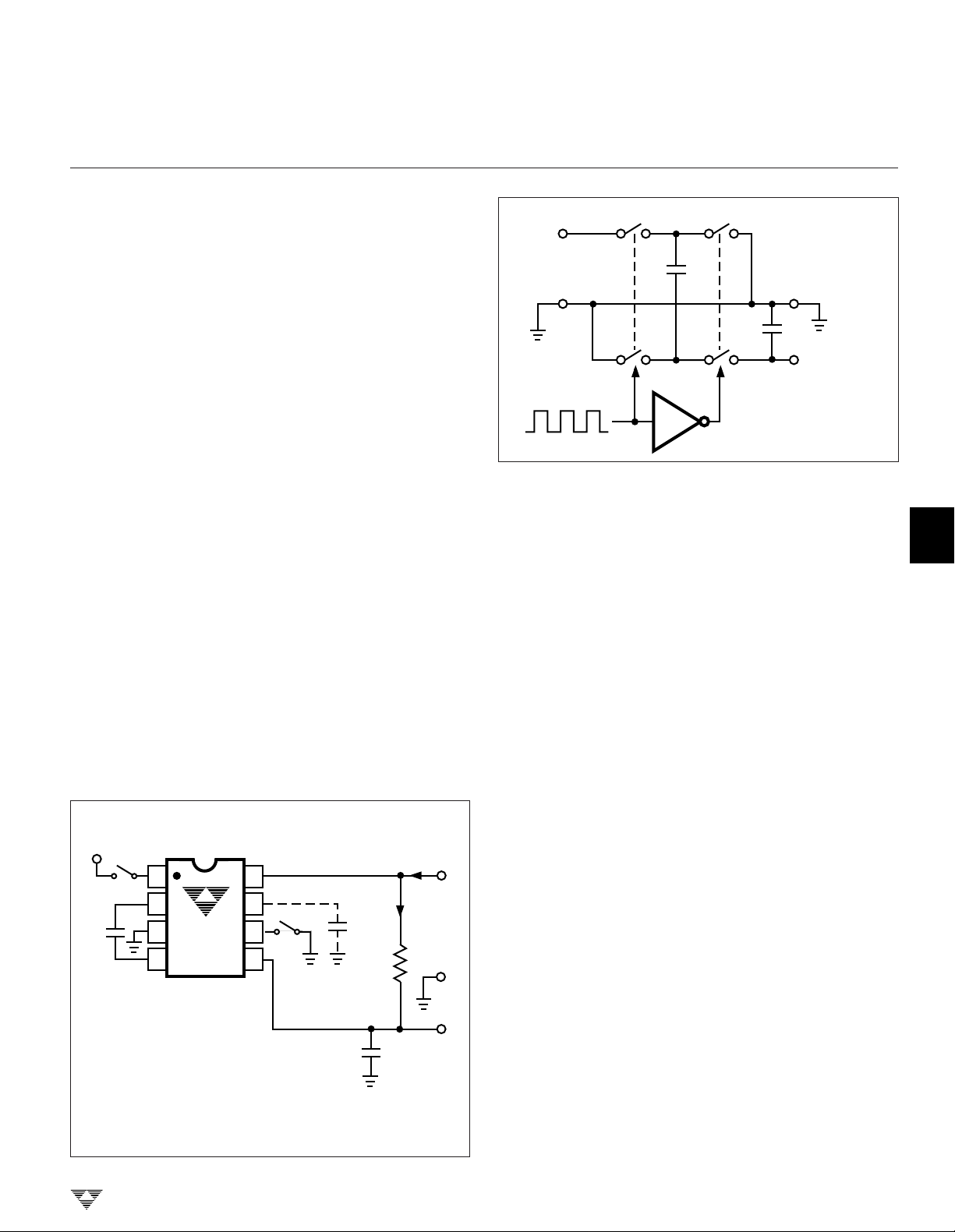
+
V
+
C
1
10µF
= V+), the output voltage must be sensed
OUT
) together
OUT
1
2
TC7660S
3
4
8
7
*
6
5
C
OSC
3
I
S
+
V
(+5V)
I
L
R
L
V
O
The voltage regulator portion of the TC7660S is an
integral part of the anti-latch-up circuitry. Its inherent voltage
drop can, however, degrade operation at low voltages. To
improve low-voltage operation, the “LV” pin should be
connected to GND, disabling the regulator. For supply
voltages greater than 3.5V, the LV terminal must be left
open to ensure latch-up-proof operation and prevent device
damage.
Theoretical Power Efficiency
Considerations
In theory, a capacitive charge pump can approach
100% efficiency if certain conditions are met:
(1) The drive circuitry consumes minimal power.
(2) The output switches have extremely low ON
(3) The impedances of the pump and reservoir
The TC7660S approaches these conditions for negative voltage multiplication if large values of C1 and C2 are
used. Energy is lost only in the transfer of charge
between capacitors if a change in voltage occurs. The
energy lost is defined by:
Figure 2. Idealized Charge Pump Inverter
resistance and virtually no offset.
capacitors are negligible at the pump frequency.
2
E = 1/2 C1 (V
1
– V
2
)
2
2
3
4
5
6
7
NOTE: For large values of C
TELCOM SEMICONDUCTOR, INC.
of C
and C2 should be increased to 100µF.
1
Figure 1. TC7660S Test Circuit
OSC
C
2
10µF
+
(>1000pF), the values
V1 and V2 are the voltages on C1 during the pump and
transfer cycles. If the impedances of C1 and C2 are relatively
high at the pump frequency (refer to Figure 2) compared to
the value of RL, there will be a substantial difference in
voltages V1 and V2. Therefore, it is desirable not only to
make C2 as large as possible to eliminate output voltage
ripple, but also to employ a correspondingly large value for
C1 in order to achieve maximum efficiency of operation.
4-71
8
 Loading...