

TelCom Semiconductor Inc TC7660HEPA, TC7660HEOA, TC7660HCPA, TC7660HCOA Datasheet
HIGH FREQUENCY 7660 DC-TO-DC VOLT AGE CONVERTER
EVALUATION
KIT
AVAILABLE
FEATURES
■ Pin Compatible with 7660, High Frequency
Performance DC-to-DC Converter
■ Low Cost, Two Low Value External Capacitors
Required ........................................................ (1.0µF)
■ Converts +5V Logic Supply to ±5V System
■ Wide Input Voltage Range ....................1.5V to 10V
■ Voltage Conversion........................................ 99.7%
■ Power Efficiency................................................ 85%
■ Available in 8-Pin SOIC and 8-Pin PDIP Packages
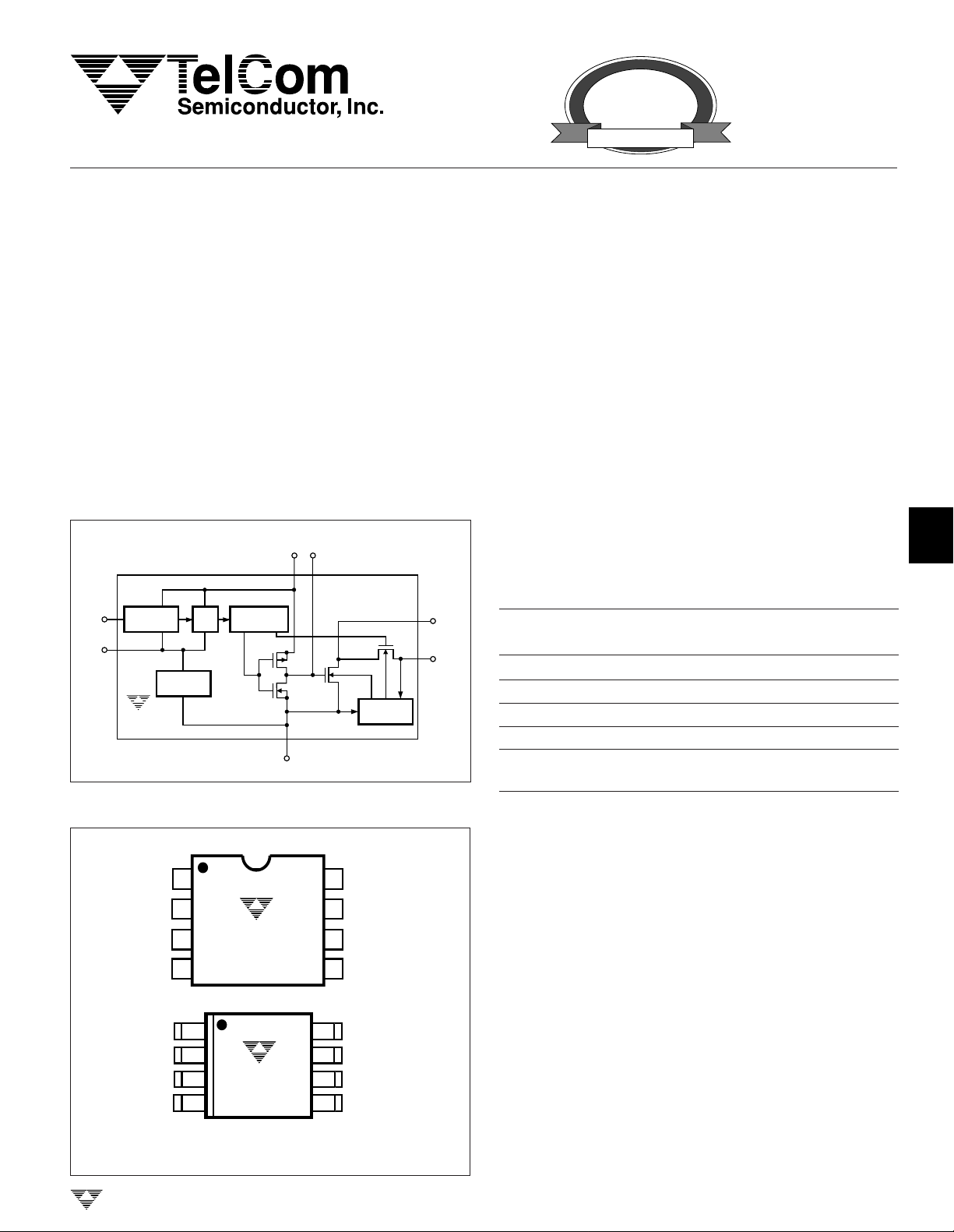
FUNCTIONAL BLOCK DIAGRAM
+
V+CAP
82
OSC
7
RC
OSCILLATOR
6
LV
INTERNAL
VOLTAGE
REGULATOR
TC7660H
÷ 2
VOLTAGE–
LEVEL
TRANSLATOR
3
GND
LOGIC
NETWORK
4
CAP
5
V
OUT
GENERAL DESCRIPTION
The TC7660H is a pin-compatible, high frequency upgrade to the Industry standard TC7660 charge pump voltage converter. It converts a +1.5V to +10V input to a
corresponding – 1.5V to -10V output using only two low-cost
capacitors, eliminating inductors and their associated cost,
size and EMI.
The TC7660H operates at a frequency of 120kHz (versus 10kHz for the TC7660), allowing the use of 1.0µF
external capacitors. Oscillator frequency can be reduced
(for lower supply current applications) by connecting an
external capacitor from OSC to ground.
The TC7660H is available in 8-pin DIP and small outline
(SOIC) packages in commercial and extended temperature
ranges.
ORDERING INFORMATION
–
Part No. Package Range
TC7660HCOA 8-Pin SOIC 0°C to +70°C
TC7660HCPA 8-Pin Plastic DIP 0°C to +70°C
TC7660HEOA 8-Pin SOIC – 40°C to +85°C
TC7660HEPA 8-Pin Plastic DIP – 40°C to +85°C
TC7660EV Evaluation Kit for
Charge Pump Family
1
TC7660H
2
3
4
Temperature
5
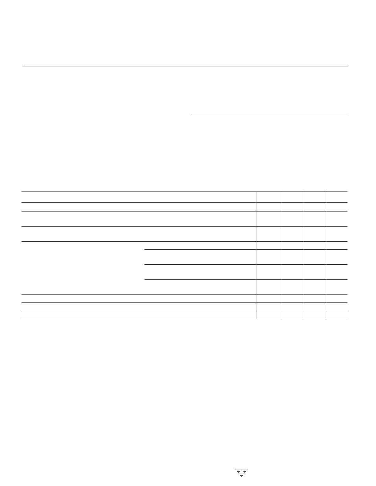
PIN CONFIGURATION (DIP and SOIC)
NC
1
+
CAP
2
3
4
1
2
3
4
TC7660HCPA
TC7660HEPA
TC7660HCOA
TC7660HEOA
TELCOM SEMICONDUCTOR, INC.
GND
–
CAP
NC
+
CAP
GND
–
CAP
NC = NO INTERNAL CONNECTION
+
8
V
OSC
7
LOW
6
VOLTAGE (LV)
V
5
OUT
+
V
8
OSC
7
LOW
6
VOLTAGE (LV)
5
V
OUT
6
7
8
TC7660H-2 10/1/96
4-63
TC7660H
HIGH FREQUENCY 7660 DC-TO-DC
VOLTAGE CONVERTER
ABSOLUTE MAXIMUM RATINGS*
Supply Voltage ...................................................... +10.5V
LV and OSC Inputs
Voltage (Note 1) ........................ – 0.3V to (V+ + 0.3V)
for V+ < 5.5V
(V+ – 5.5V) to (V+ + 0.3V)
for V+ > 5.5V
Current Into LV (Note 1)......................20µA for V+ > 3.5V
Output Short Duration (V
≤ 5.5V) .........Continuous
SUPPLY
Power Dissipation (TA ≤ 70°C) (Note 2)
SOIC...............................................................470mW
Plastic DIP ......................................................730mW
ELECTRICAL CHARACTERISTICS: Over Operating Temperature Range with V
Operating Temperature Range
C Suffix ..................................................0°C to +70°C
E Suffix ............................................. – 40°C to +85°C
Storage Temperature Range ................– 65°C to +150°C
Lead Temperature (Soldering, 10 sec) .................+300°C
*Static-sensitive device. Unused devices must be stored in conductive
material. Protect devices from static discharge and static fields. Stresses
above those listed under "Absolute Maximum Ratings" may cause permanent damage to the device. These are stress ratings only and functional
operation of the device at these or any other conditions above those
indicated in the operation sections of the specifications is not implied.
Exposure to absolute maximum rating conditions for extended periods
may affect device reliability.
+
= 5V, CI = C2 = 1µF,C
OSC
= 0,
Test Circuit (Figure 1), unless otherwise indicated.
Symbol Parameter Test Conditions Min Typ Max Unit
+
I
+
V
H
+
V
L
R
OUT
F
OSC
P
EFF
V
EFF
NOTES: 1. Connecting any input terminal to voltages greater than V+ or less than GND may cause destructive latch-up. It is recommended that no
Supply Current RL = ∞ — 0.46 1.0 mA
Supply Voltage Range, High Min ≤ TA ≤ Max, 3 — 10 V
RL = 5kΩ, LV Open
Supply Voltage Range, Low Min ≤ TA ≤ Max, 1.5 — 3.5 V
RL = 5kΩ, LV to GND
Output Source Resistance I
= 20mA, TA = 25°C — 55 80 Ω
OUT
I
= 20mA, 0°C ≤ TA ≤ +70°C——95Ω
OUT
(C Device)
I
= 20mA, – 40°C ≤ TA ≤ +85°C — — 110 Ω
OUT
(E Device)
+
V
= 2V, I
= 3mA, LV to GND — 150 250 Ω
OUT
0°C ≤ TA ≤ +70°C
Oscillator Frequency — 120 — kHz
Power Efficiency I
= 10mA, Min ≤ TA ≤ Max 81 85 — %
OUT
Voltage Efficiency RL = ∞ 99 99.7 — %
inputs from sources operating from external supplies be applied prior to "power up" of the TC7660H.
2. Derate linearly above 50°C by 5.5 mW/°C.
4-64
TELCOM SEMICONDUCTOR, INC.
 Loading...