

TelCom Semiconductor Inc TC7135CLI, TC7135CBU, TC7135CPI Datasheet
4-1/2 DIGIT ANALOG-TO-DIGITAL CONVERTER
1
TC7135
FEATURES
■ Low Roll-Over Error ......................... ±1 Count Max
■ Guaranteed Nonlinearity Error ........ ±1 Count Max
■ Guaranteed Zero Reading for 0V Input
■ True Polarity Indication at Zero for Null Detection
■ Multiplexed BCD Data Output
■ TTL-Compatible Outputs
■ Differential Input
■ Control Signals Permit Interface to UARTs and
µProcessors
■ Auto-Ranging Supported With Overrange and
Underrange Signals
■ Blinking Display Visually Indicates Overrange
Condition
■ Low Input Current............................................. 1 pA
■ Low Zero Reading Drift ............................... 2 µV/°C
■ Interfaces to TC7211A (LCD) and TC7212A (LED)
Display Drivers
■ Available in DIP and Surface-Mount Packages
GENERAL DESCRIPTION
The TC7135 4-1/2 digit analog-to-digital converter (ADC)
offers 50 ppm (1 part in 20,000) resolution with a maximum
nonlinearity error of 1 count. An auto-zero cycle reduces zero
error to below 10 µV and zero drift to 0.5 µV/°C. Source
impedance errors are minimized by a 10 pA maximum input
current. Roll-over error is limited to ±1 count.
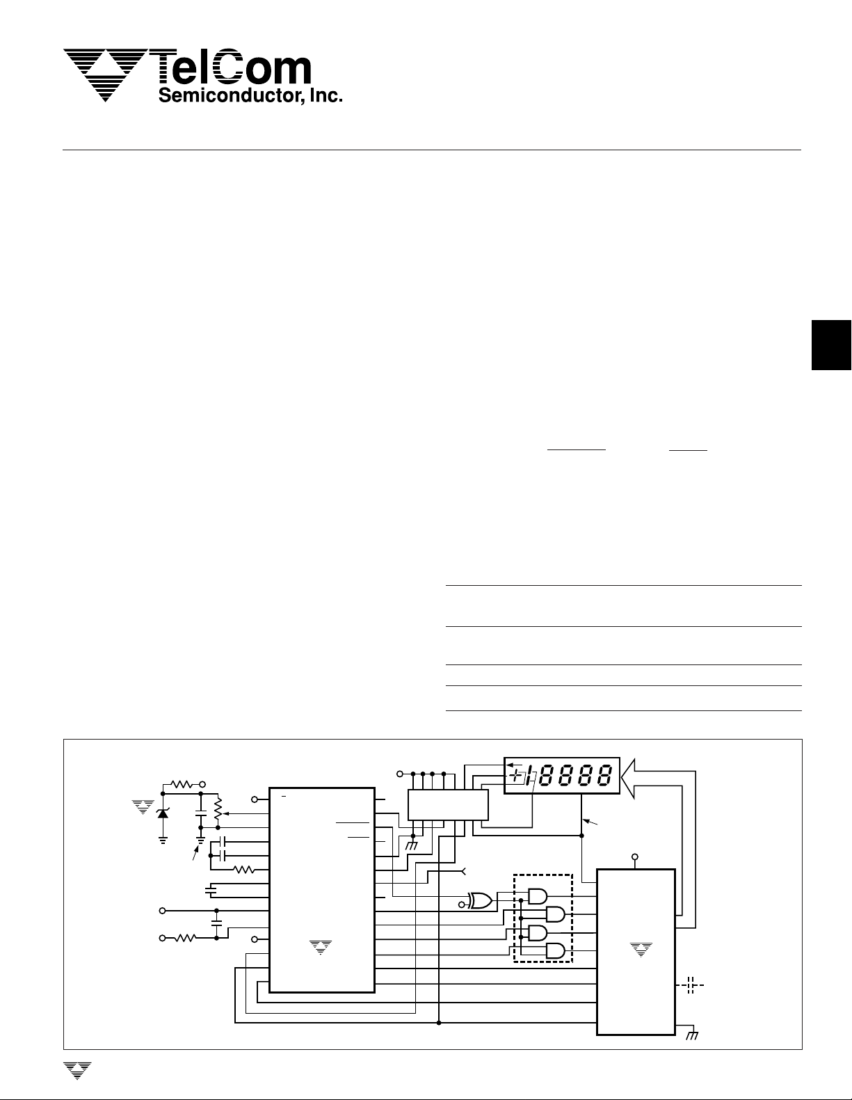
By combining the TC7135 with a TC7211A (LCD) or
TC7212A (LED) driver, a 4-1/2 digit display DVM or DPM can
be constructed. Overrange and underrange signals support
automatic range switching and special display blanking/flashing applications.
Microprocessor-based measurement systems are supported by BUSY, STROBE, and RUN/HOLD control signals.
Remote data acquisition systems with data transfer via UARTs
are also possible. The additional control pins and multiplexed
BCD outputs make the TC7135 the ideal converter for display or microprocessor-based measurement systems.
ORDERING INFORMATION
Temperature
Part No. Package Range
TC7135CBU 64-Pin Plastic 0°C to +70°C
Flat Package
TC7135CLI 28-Pin PLCC 0°C to +70°C
2
3
4
5
TYPICAL 4-1/2 DIGIT DVM WITH LCD
6.8 kΩ
+5V
0.1 µF
TC04
ANALOG
GROUND
1 µF
100 kΩ
0.1
µF
INPUT
TELCOM SEMICONDUCTOR, INC.
–5V
100 kΩ
0.47 µF
1 µF
100 kΩ
+5V
1
2
3
4
5
6
7
8
9
10
11
12
13
14
V
REF IN
ANALOG
COMMON
INT OUT
AZ IN
BUFF OUT
–
C
REF
+
C
REF
–INPUT
+INPUT
+
V
D5
TC7135
B1
B2
STROBE
RUN/HOLD
CLOCK
UR
OR
DGND
POL
BUSY
D1
D2
D3
D4
B8
B4
+5V
28
27
26
25
24
23
22
21
20
19
18
17
16
15
TC7135CPI 28-Pin Plastic DIP 0°C to +70°C
4-1/2 DIGIT LCD
1161514125 3 4
CD4054A
7 8 131110 9 2 6
120 Hz = 3 READING/SEC
CLOCK IN
1/4 CD4030
+5V
CD4081
BACKPLANE
5
BP
31
1
D
32
2
D
33
3
D
34
4
D
30
B
3
29
B
2
28
B
1
27
B
0
SEGMENT
+5V
1
+
V
TC7211A
SEG
OUT
OSC
GND
D
R
I
V
E
2,3,4
6–26
37–40
36
+5V
OPTIONAL
CAP
35
6
7
8
TC7135-10 11/6/96
3-113

TC7135
4-1/2 DIGIT
ANALOG-TO-DIGITAL CONVERTER
ABSOLUTE MAXIMUM RATINGS* (Note 1)
Positive Supply Voltage ............................................. +6V
Negative Supply Voltage.............................................–9V
Analog Input Voltage (Pin 9 or 10) ......... V+ to V– (Note 2)
Reference Input Voltage (Pin 2)........................... V+ to V
Clock Input Voltage ..............................................0V to V
Operating Temperature Range ....................0°C to +70°C
Storage Temperature Range .................–65°C to +160°C
ELECTRICAL CHARACTERISTICS: T
= +25°C, f
A
Lead Temperature (Soldering, 10 sec) .................+300°C
Package Power Dissipation (TA ≤ 70°C)
Plastic DIP ........................................................1.14W
PLCC ................................................................1.00W
–
+
Plastic Flat Package .........................................1.14W
*Static-sensitive device. Unused devices must be stored in conductive
material to protect them from static discharge and static fields. Stresses
above those listed under "Absolute Maximum Ratings" may cause permanent damage to the device. These are stress ratings only and functional
operation of the device at these or any other conditions above those
indicated in the operational sections of the specifications is not implied.
= 120 kHz, V+ = +5V, V– = –5V (Figure 1)
CLOCK
Symbol Parameter Test Conditions Min Typ Max Unit
Analog
Display Reading With Notes 2 and 3 –0.0000 ±0.0000 +0.0000 Display
Zero Volt Input Reading
TC
Z
TC
FS
NL Nonlinearity Error Note 6 — 0.5 1 Count
DNL Differential Linearity Error Note 6 — 0.01 — LSB
±FSE ± Full-Scale Symmetry –VIN = +V
I
IN
V
N
Digital
I
IL
I
IH
V
OL
V
OH
f
CLK
Power Supply
+
V
–
V
+
I
–
I
PD Power Dissipation f
NOTES: 1. Limit input current to under 100µA if input
Zero Reading Temperature VIN = 0V — 0.5 2 µV/°C
Coefficient Note 4
Full-Scale Temperature VIN = 2V — — 5 ppm/°C
Coefficient Notes 4 and 5
Display Reading in VIN = V
REF
+0.9996 +0.9999 +1.0000 Display
Ratiometric Operation Note 2 Reading
IN
— 0.5 1 Count
Error (Roll-Over Error) Note 7
Input Leakage Current Note 3 — 1 10 pA
Noise Peak-to-Peak Value Not — 15 — µV
Exceeded 95% of Time
Input Low Current VIN = 0V — 10 100 µA
Input High Current VIN = +5V — 0.08 10 µA
Output Low Voltage IOL = 1.6 mA — 0.2 0.4 V
Output High Voltage
B
, B2, B4, B8, D1–D
1
5
Busy, Polarity, Overrange, I
IOH = 1 mA 2.4 4.4 5 V
= 10 µA 4.9 4.99 5 V
OH
Underrange, Strobe
Clock Frequency Note 8 0 120 1200 kHz
Positive Supply Voltage 4 5 6 V
Negative Supply Voltage –3 –5 –8 V
Positive Supply Current f
Negative Supply Current f
voltages exceed supply voltage.
2. Full-scale voltage = 2V.
3. VIN = 0V.
4. 0°C ≤ TA ≤ +70°C.
= 0 Hz — 1 3 mA
CLK
= 0 Hz — 0.7 3 mA
CLK
= 0 Hz — 8.5 30 mW
CLK
5. External reference temperature coefficient less than 0.01 ppm/°C.
6. –2V ≤ VIN ≤ +2V. Error of reading from best fit straight line.
7. |VIN| = 1.9959.
8. Specification related to clock frequency range over which the
TC7135 correctly performs its various functions. Increased errors
result at higher operating frequencies.
P-P
3-114
TELCOM SEMICONDUCTOR, INC.
4-1/2 DIGIT
ANALOG-TO-DIGITAL CONVERTER
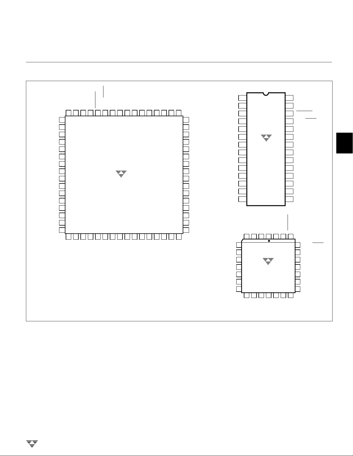
PIN CONFIGURATIONS
NC
NC
NC
NC
NC
NC
OVERRANGE
UNDERRANGE
NC
V
REF IN
ANALOG COM
NC
NC
NC
NC
NCNCNC
NC
63 61 60 59 58 57 56 55 545352 51 50 4964
62
1
●
2
3
4
5
6
7
8
9
–
10
11
12
13
14
15
16
17 18 19 20 21 22 23 24 25 26 27 28 29 30 31
NC
INT OUT
NOTES: 1. NC = No internal connection.
NC
AZ IN
STROBE
RUN/HOLD
TC7135CBU
(NOTES 1)
NC
–
BUFF OUT
DGND
(PFP)
REF
C
POL
NC
NC
NC
+
CLOCK IN
BUSYD2D1
NC
REF
C
–INPUT
NC
NC
NC
NC
+INPUT
1
TC7135
2
–
V
1
NC
48
NC
47
NC
46
NC
45
D3
44
D4
43
B8
42
B4
41
B2
40
NC
39
B1
38
D5
37
NC
36
NC
35
NC
34
NC
33
NC
32
+
V
REF IN
ANALOG
INT OUT
BUFF OUT
–
+
(MSD) D5
(LSB) B1
AZ IN
BUFF OUT
REF CAP
REF CAP
–
INPUT
+
INPUT
COM
AZ IN
–
C
REF
+
C
REF
INPUT
INPUT
V
B2
–
+
+
V
2
3
4
5
6
7
TC7135CPI
8
9
10
+
11
12
13
14
5
6
7
8
9
10
11
(PDIP)
INT OUT
ANALOG
COM
REF IN
4 3 2 1 27 2628
TC7135CLI
(PLCC)
12 13 14 15 17 18
B2
D5
B1
(LSB)
(MSD)
–
URORSTROBE
V
16
B4
(MSB)
B8
28
27
26
25
24
23
22
21
20
19
18
17
16
15
D4
UNDERRANGE
OVERRANGE
STROBE
RUN/HOLD
DIGTAL GND
POLARITY
CLOCK IN
BUSY
D1 (LSD)
D2
D3
D4
B8 (MSB)
B4
25
RUN/HOLD
24
DIGTAL GND
23
POLARITY
22
CLOCK IN
21
BUSY
20
D1 (LSD)
19
D2
D3
3
4
5
6
TELCOM SEMICONDUCTOR, INC.
7
8
3-115
TC7135
4-1/2 DIGIT
ANALOG-TO-DIGITAL CONVERTER
SET V
V
REF
REF
IN
= 1V
100 kΩ
ANALOG GND
0.47
µF
100 kΩ
SIGNAL
INPUT
+
5V
100
kΩ
LOGIC
INPUT
0.1 µF
–5V
1
–
V
2
REF IN
3
ANALOG
COMMON
4
1 µF
5
6
7
8
9
10
11
12
13
14
INT OUT
AZ IN
BUFF OUT
–
C
REF
+
C
REF
–
INPUT
+
INPUT
+
V
D5 (MSD)
B1 (LSB)
B2
1 µF
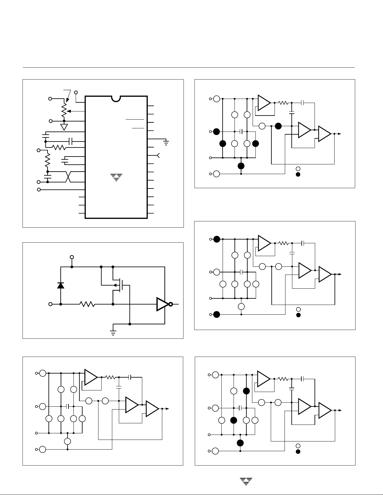
Figure 1. Test Circuit
+
V
UNDERRANGE
OVERRANGE
STROBE
RUN/HOLD
DIGTAL GND
POLARITY
CLOCK IN
(LSD) D1
TC7135
(MSB) B8
BUSY
D2
D3
D4
B4
28
27
26
25
24
23
22
21
20
19
18
17
16
15
BUFFER
CLOCK
INPUT
120 kHz
+
IN
REF
IN
ANALOG
COM
–
IN
+
IN
REF
IN
ANALOG
COM
–
IN
SW
SW
SW
SW
SW
SW
SW
SW
ANALOG
SW
C
REF
SW
INPUT BUFFER
+
RI
–
RI
SW
1
+
–
SWIZSW
SW
Z
R
Z
INT
C
INT
C
SZ
–
+
INTEGRATOR
SWITCH OPEN
SWITCH CLOSED
COMPARATOR
+
–
TO
DIGITAL
SECTION
I
–
SW
RI
R
Z
+
SW
RI
I
Figure 3B. System Zero Phase
ANALOG
SW
C
REF
SW
INPUT BUFFER
+
RI
–
RI
SW
1
+
–
SWIZSW
SW
Z
R
INT
Z
C
INT
C
SZ
–
+
INTEGRATOR
SWITCH OPEN
SWITCH CLOSED
COMPARATOR
+
–
TO
DIGITAL
SECTION
I
–
SW
RI
R
Z
+
SW
RI
I
+
IN
REF
IN
ANALOG
COM
–
IN
3-116
SW
SW
SW
SW
Figure 2. Digital Logic Input
ANALOG
SW
C
REF
SW
INPUT BUFFER
+
RI
–
RI
SW
1
+
–
SWIZSW
SW
Z
I
–
SW
RI
R
Z
+
SW
RI
I
Figure 3A. Internal Analog Switches
R
INT
Z
C
INT
C
SZ
–
+
INTEGRATOR
COMPARATOR
+
–
TO
DIGITAL
SECTION
+
IN
REF
IN
ANALOG
COM
–
IN
Figure 3C. Input Signal Integration Phase
ANALOG
SW
C
REF
SW
INPUT BUFFER
+
RI
–
RI
SW
1
+
–
SWIZSW
SW
Z
R
INT
Z
C
INT
C
SZ
–
+
INTEGRATOR
SWITCH OPEN
SWITCH CLOSED
SW
SW
SW
SW
I
–
SW
RI
R
Z
+
SW
RI
I
Figure 3D. Reference Voltage Integration Phase
TELCOM SEMICONDUCTOR, INC.
COMPARATOR
+
–
TO
DIGITAL
SECTION
 Loading...