

4-1/2 DIGIT ANALOG-TO-DIGITAL CONVERTER
1
TC7135
FEATURES
■ Low Roll-Over Error ......................... ±1 Count Max
■ Guaranteed Nonlinearity Error ........ ±1 Count Max
■ Guaranteed Zero Reading for 0V Input
■ True Polarity Indication at Zero for Null Detection
■ Multiplexed BCD Data Output
■ TTL-Compatible Outputs
■ Differential Input
■ Control Signals Permit Interface to UARTs and
µProcessors
■ Auto-Ranging Supported With Overrange and
Underrange Signals
■ Blinking Display Visually Indicates Overrange
Condition
■ Low Input Current............................................. 1 pA
■ Low Zero Reading Drift ............................... 2 µV/°C
■ Interfaces to TC7211A (LCD) and TC7212A (LED)
Display Drivers
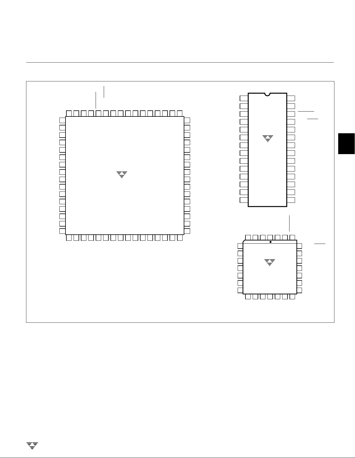
■ Available in DIP and Surface-Mount Packages
GENERAL DESCRIPTION
The TC7135 4-1/2 digit analog-to-digital converter (ADC)
offers 50 ppm (1 part in 20,000) resolution with a maximum
nonlinearity error of 1 count. An auto-zero cycle reduces zero
error to below 10 µV and zero drift to 0.5 µV/°C. Source
impedance errors are minimized by a 10 pA maximum input
current. Roll-over error is limited to ±1 count.
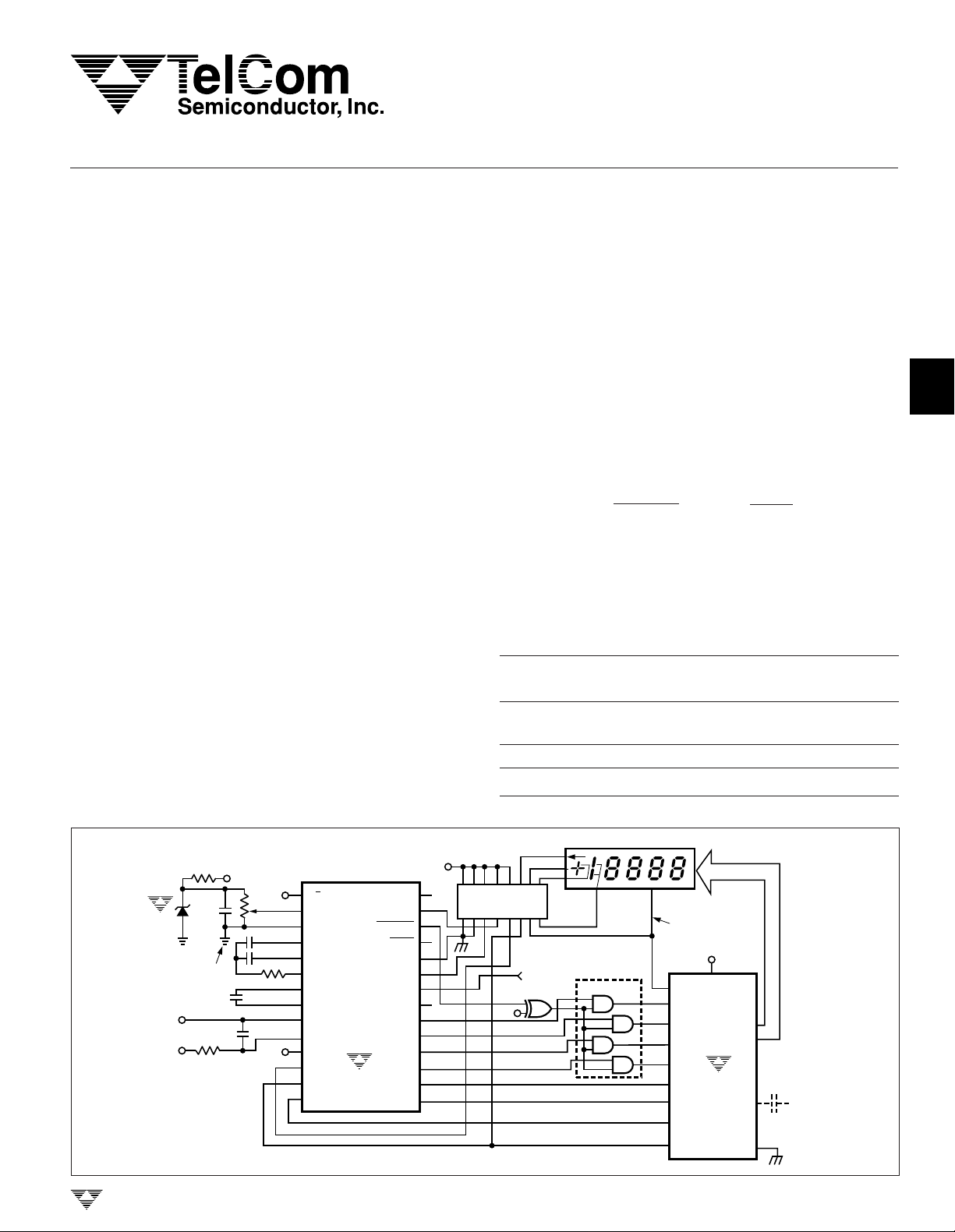
By combining the TC7135 with a TC7211A (LCD) or
TC7212A (LED) driver, a 4-1/2 digit display DVM or DPM can
be constructed. Overrange and underrange signals support
automatic range switching and special display blanking/flashing applications.
Microprocessor-based measurement systems are supported by BUSY, STROBE, and RUN/HOLD control signals.
Remote data acquisition systems with data transfer via UARTs
are also possible. The additional control pins and multiplexed
BCD outputs make the TC7135 the ideal converter for display or microprocessor-based measurement systems.
ORDERING INFORMATION
Temperature
Part No. Package Range
TC7135CBU 64-Pin Plastic 0°C to +70°C
Flat Package
TC7135CLI 28-Pin PLCC 0°C to +70°C
2
3
4
5
TYPICAL 4-1/2 DIGIT DVM WITH LCD
6.8 kΩ
+5V
0.1 µF
TC04
ANALOG
GROUND
1 µF
100 kΩ
0.1
µF
INPUT
TELCOM SEMICONDUCTOR, INC.
–5V
100 kΩ
0.47 µF
1 µF
100 kΩ
+5V
1
2
3
4
5
6
7
8
9
10
11
12
13
14
V
REF IN
ANALOG
COMMON
INT OUT
AZ IN
BUFF OUT
–
C
REF
+
C
REF
–INPUT
+INPUT
+
V
D5
TC7135
B1
B2
STROBE
RUN/HOLD
CLOCK
UR
OR
DGND
POL
BUSY
D1
D2
D3
D4
B8
B4
+5V
28
27
26
25
24
23
22
21
20
19
18
17
16
15
TC7135CPI 28-Pin Plastic DIP 0°C to +70°C
4-1/2 DIGIT LCD
1161514125 3 4
CD4054A
7 8 131110 9 2 6
120 Hz = 3 READING/SEC
CLOCK IN
1/4 CD4030
+5V
CD4081
BACKPLANE
5
BP
31
1
D
32
2
D
33
3
D
34
4
D
30
B
3
29
B
2
28
B
1
27
B
0
SEGMENT
+5V
1
+
V
TC7211A
SEG
OUT
OSC
GND
D
R
I
V
E
2,3,4
6–26
37–40
36
+5V
OPTIONAL
CAP
35
6
7
8
TC7135-10 11/6/96
3-113

TC7135
4-1/2 DIGIT
ANALOG-TO-DIGITAL CONVERTER
ABSOLUTE MAXIMUM RATINGS* (Note 1)
Positive Supply Voltage ............................................. +6V
Negative Supply Voltage.............................................–9V
Analog Input Voltage (Pin 9 or 10) ......... V+ to V– (Note 2)
Reference Input Voltage (Pin 2)........................... V+ to V
Clock Input Voltage ..............................................0V to V
Operating Temperature Range ....................0°C to +70°C
Storage Temperature Range .................–65°C to +160°C
ELECTRICAL CHARACTERISTICS: T
= +25°C, f
A
Lead Temperature (Soldering, 10 sec) .................+300°C
Package Power Dissipation (TA ≤ 70°C)
Plastic DIP ........................................................1.14W
PLCC ................................................................1.00W
–
+
Plastic Flat Package .........................................1.14W
*Static-sensitive device. Unused devices must be stored in conductive
material to protect them from static discharge and static fields. Stresses
above those listed under "Absolute Maximum Ratings" may cause permanent damage to the device. These are stress ratings only and functional
operation of the device at these or any other conditions above those
indicated in the operational sections of the specifications is not implied.
= 120 kHz, V+ = +5V, V– = –5V (Figure 1)
CLOCK
Symbol Parameter Test Conditions Min Typ Max Unit
Analog
Display Reading With Notes 2 and 3 –0.0000 ±0.0000 +0.0000 Display
Zero Volt Input Reading
TC
Z
TC
FS
NL Nonlinearity Error Note 6 — 0.5 1 Count
DNL Differential Linearity Error Note 6 — 0.01 — LSB
±FSE ± Full-Scale Symmetry –VIN = +V
I
IN
V
N
Digital
I
IL
I
IH
V
OL
V
OH
f
CLK
Power Supply
+
V
–
V
+
I
–
I
PD Power Dissipation f
NOTES: 1. Limit input current to under 100µA if input
Zero Reading Temperature VIN = 0V — 0.5 2 µV/°C
Coefficient Note 4
Full-Scale Temperature VIN = 2V — — 5 ppm/°C
Coefficient Notes 4 and 5
Display Reading in VIN = V
REF
+0.9996 +0.9999 +1.0000 Display
Ratiometric Operation Note 2 Reading
IN
— 0.5 1 Count
Error (Roll-Over Error) Note 7
Input Leakage Current Note 3 — 1 10 pA
Noise Peak-to-Peak Value Not — 15 — µV
Exceeded 95% of Time
Input Low Current VIN = 0V — 10 100 µA
Input High Current VIN = +5V — 0.08 10 µA
Output Low Voltage IOL = 1.6 mA — 0.2 0.4 V
Output High Voltage
B
, B2, B4, B8, D1–D
1
5
Busy, Polarity, Overrange, I
IOH = 1 mA 2.4 4.4 5 V
= 10 µA 4.9 4.99 5 V
OH
Underrange, Strobe
Clock Frequency Note 8 0 120 1200 kHz
Positive Supply Voltage 4 5 6 V
Negative Supply Voltage –3 –5 –8 V
Positive Supply Current f
Negative Supply Current f
voltages exceed supply voltage.
2. Full-scale voltage = 2V.
3. VIN = 0V.
4. 0°C ≤ TA ≤ +70°C.
= 0 Hz — 1 3 mA
CLK
= 0 Hz — 0.7 3 mA
CLK
= 0 Hz — 8.5 30 mW
CLK
5. External reference temperature coefficient less than 0.01 ppm/°C.
6. –2V ≤ VIN ≤ +2V. Error of reading from best fit straight line.
7. |VIN| = 1.9959.
8. Specification related to clock frequency range over which the
TC7135 correctly performs its various functions. Increased errors
result at higher operating frequencies.
P-P
3-114
TELCOM SEMICONDUCTOR, INC.
4-1/2 DIGIT
ANALOG-TO-DIGITAL CONVERTER
PIN CONFIGURATIONS
NC
NC
NC
NC
NC
NC
OVERRANGE
UNDERRANGE
NC
V
REF IN
ANALOG COM
NC
NC
NC
NC
NCNCNC
NC
63 61 60 59 58 57 56 55 545352 51 50 4964
62
1
●
2
3
4
5
6
7
8
9
–
10
11
12
13
14
15
16
17 18 19 20 21 22 23 24 25 26 27 28 29 30 31
NC
INT OUT
NOTES: 1. NC = No internal connection.
NC
AZ IN
STROBE
RUN/HOLD
TC7135CBU
(NOTES 1)
NC
–
BUFF OUT
DGND
(PFP)
REF
C
POL
NC
NC
NC
+
CLOCK IN
BUSYD2D1
NC
REF
C
–INPUT
NC
NC
NC
NC
+INPUT
1
TC7135
2
–
V
1
NC
48
NC
47
NC
46
NC
45
D3
44
D4
43
B8
42
B4
41
B2
40
NC
39
B1
38
D5
37
NC
36
NC
35
NC
34
NC
33
NC
32
+
V
REF IN
ANALOG
INT OUT
BUFF OUT
–
+
(MSD) D5
(LSB) B1
AZ IN
BUFF OUT
REF CAP
REF CAP
–
INPUT
+
INPUT
COM
AZ IN
–
C
REF
+
C
REF
INPUT
INPUT
V
B2
–
+
+
V
2
3
4
5
6
7
TC7135CPI
8
9
10
+
11
12
13
14
5
6
7
8
9
10
11
(PDIP)
INT OUT
ANALOG
COM
REF IN
4 3 2 1 27 2628
TC7135CLI
(PLCC)
12 13 14 15 17 18
B2
D5
B1
(LSB)
(MSD)
–
URORSTROBE
V
16
B4
(MSB)
B8
28
27
26
25
24
23
22
21
20
19
18
17
16
15
D4
UNDERRANGE
OVERRANGE
STROBE
RUN/HOLD
DIGTAL GND
POLARITY
CLOCK IN
BUSY
D1 (LSD)
D2
D3
D4
B8 (MSB)
B4
25
RUN/HOLD
24
DIGTAL GND
23
POLARITY
22
CLOCK IN
21
BUSY
20
D1 (LSD)
19
D2
D3
3
4
5
6
TELCOM SEMICONDUCTOR, INC.
7
8
3-115
TC7135
4-1/2 DIGIT
ANALOG-TO-DIGITAL CONVERTER
SET V
V
REF
REF
IN
= 1V
100 kΩ
ANALOG GND
0.47
µF
100 kΩ
SIGNAL
INPUT
+
5V
100
kΩ
LOGIC
INPUT
0.1 µF
–5V
1
–
V
2
REF IN
3
ANALOG
COMMON
4
1 µF
5
6
7
8
9
10
11
12
13
14
INT OUT
AZ IN
BUFF OUT
–
C
REF
+
C
REF
–
INPUT
+
INPUT
+
V
D5 (MSD)
B1 (LSB)
B2
1 µF
Figure 1. Test Circuit
+
V
UNDERRANGE
OVERRANGE
STROBE
RUN/HOLD
DIGTAL GND
POLARITY
CLOCK IN
(LSD) D1
TC7135
(MSB) B8
BUSY
D2
D3
D4
B4
28
27
26
25
24
23
22
21
20
19
18
17
16
15
BUFFER
CLOCK
INPUT
120 kHz
+
IN
REF
IN
ANALOG
COM
–
IN
+
IN
REF
IN
ANALOG
COM
–
IN
SW
SW
SW
SW
SW
SW
SW
SW
ANALOG
SW
C
REF
SW
INPUT BUFFER
+
RI
–
RI
SW
1
+
–
SWIZSW
SW
Z
R
Z
INT
C
INT
C
SZ
–
+
INTEGRATOR
SWITCH OPEN
SWITCH CLOSED
COMPARATOR
+
–
TO
DIGITAL
SECTION
I
–
SW
RI
R
Z
+
SW
RI
I
Figure 3B. System Zero Phase
ANALOG
SW
C
REF
SW
INPUT BUFFER
+
RI
–
RI
SW
1
+
–
SWIZSW
SW
Z
R
INT
Z
C
INT
C
SZ
–
+
INTEGRATOR
SWITCH OPEN
SWITCH CLOSED
COMPARATOR
+
–
TO
DIGITAL
SECTION
I
–
SW
RI
R
Z
+
SW
RI
I
+
IN
REF
IN
ANALOG
COM
–
IN
3-116
SW
SW
SW
SW
Figure 2. Digital Logic Input
ANALOG
SW
C
REF
SW
INPUT BUFFER
+
RI
–
RI
SW
1
+
–
SWIZSW
SW
Z
I
–
SW
RI
R
Z
+
SW
RI
I
Figure 3A. Internal Analog Switches
R
INT
Z
C
INT
C
SZ
–
+
INTEGRATOR
COMPARATOR
+
–
TO
DIGITAL
SECTION
+
IN
REF
IN
ANALOG
COM
–
IN
Figure 3C. Input Signal Integration Phase
ANALOG
SW
C
REF
SW
INPUT BUFFER
+
RI
–
RI
SW
1
+
–
SWIZSW
SW
Z
R
INT
Z
C
INT
C
SZ
–
+
INTEGRATOR
SWITCH OPEN
SWITCH CLOSED
SW
SW
SW
SW
I
–
SW
RI
R
Z
+
SW
RI
I
Figure 3D. Reference Voltage Integration Phase
TELCOM SEMICONDUCTOR, INC.
COMPARATOR
+
–
TO
DIGITAL
SECTION

4-1/2 DIGIT
+
–
REF
VOLTAGE
ANALOG
INPUT
SIGNAL
+
–
DISPLAY
SWITCH
DRIVER
CONTROL
LOGIC
INTEGRATOR
OUTPUT
CLOCK
COUNTER
POLARITY CONTROL
PHASE
CONTROL
V
IN
V
IN
V
FULL SCALE
1/2 V
FULL SCALE
VARIABLE
REFERENCE
INTEGRATE
TIME
FIXED
SIGNAL
INTEGRATE
TIME
INTEGRATOR
COMPARATOR
'
'
ANALOG-TO-DIGITAL CONVERTER
1
TC7135
ANALOG
SW
C
REF
SW
INPUT BUFFER
+
RI
–
RI
SW
1
+
–
SWIZSW
SW
Z
R
INT
Z
C
INT
C
SZ
–
+
INTEGRATOR
SWITCH OPEN
SWITCH CLOSED
COMPARATOR
+
–
TO
DIGITAL
SECTION
+
IN
REF
IN
ANALOG
COM
–
IN
SW
I
–
SW
RI
SW
R
SW
Z
+
SW
RI
SW
I
Figure 3E. Integrator Output Zero Phase
GENERAL THEORY OF OPERATION
(All Pin Designations Refer to 28-Pin DIP)
Dual-Slope Conversion Principles
The TC7135 is a dual-slope, integrating analog-todigital converter. An understanding of the dual-slope conversion technique will aid in following detailed TC7135
operational theory.
The conventional dual-slope converter measurement
cycle has two distinct phases:
For a constant VIN:
t
VIN = V
RI
.
R
[]
t
SI
The dual-slope converter accuracy is unrelated to the
integrating resistor and capacitor values, as long as they are
stable during a measurement cycle. Noise immunity is an
inherent benefit. Noise spikes are integrated, or averaged,
to zero during integration periods. Integrating ADCs are
immune to the large conversion errors that plague successive approximation converters in high-noise environments.
(See Figure 4.)
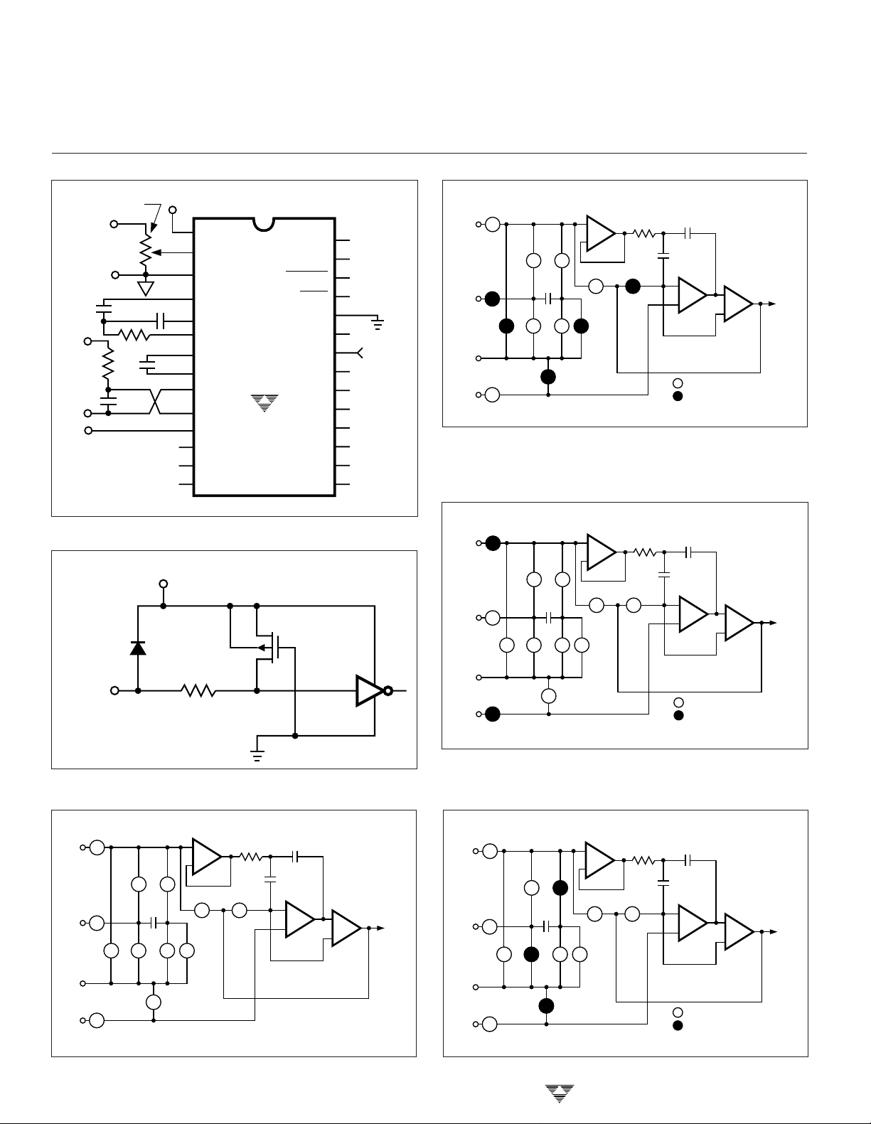
TC7135 Operational Theory
The TC7135 incorporates a system zero phase and
integrator output voltage zero phase to the normal twophase dual-slope measurement cycle. Reduced system
errors, fewer calibration steps, and a shorter overrange
recovery time result.
The TC7135 measurement cycle contains four phases:
(1) System zero
(2) Analog input signal integration
(3) Reference voltage integration
(4) Integrator output zero
Internal analog gate status for each phase is shown in
Table 1.
2
3
4
5
(1) Input signal integration
(2) Reference voltage integration (deintegration)
The input signal being converted is integrated for a fixed
time period, measured by counting clock pulses. An opposite polarity constant reference voltage is then integrated
until the integrator output voltage returns to zero. The
reference integration time is directly proportional to the input
signal.
requires the integrator output to "ramp-up" and "ramp-
In a simple dual-slope converter, a complete conversion
down."
A simple mathematical equation relates the input signal,
reference voltage, and integration time:
where:
t
1V
RC RC
SI
∫
0
VIN(t) dt = ,
t
R
RI
VR= Reference voltage
tSI= Signal integration time (fixed)
tRI= Reference voltage integration time (variable).
TELCOM SEMICONDUCTOR, INC.
Figure 4. Basic Dual-Slope Converter
6
7
8
3-117

TC7135
Table 1. Internal Analog Gate Status
4-1/2 DIGIT
ANALOG-TO-DIGITAL CONVERTER
Conversion Reference
Cycle Phase SW
System Zero Closed Closed Closed 3B
Input Signal Closed 3C
Integration
Reference Voltage Closed* Closed 3D
Integration
Integrator Closed Closed 3E
Output Zero
*NOTE: Assumes a positive polarity input signal. SW
I
SW
System Zero Phase
During this phase, errors due to buffer, integrator, and
comparator offset voltages are compensated for by charging CAZ (auto-zero capacitor) with a compensating error
voltage. With zero input voltage, the integrator output remains at zero.
The external input signal is disconnected from the
internal circuitry by opening the two SWI switches. The
internal input points connect to analog common. The reference capacitor charges to the reference voltage potential
through SWR. A feedback loop, closed around the integrator
and comparator, charges the CAZ with a voltage to compensate for buffer amplifier, integrator, and comparator offset
voltages. (See Figure 3B.)
Analog Input Signal Integration Phase
The TC7135 integrates the differential voltage between
the +INPUT and –INPUT. The differential voltage must be
within the device's common-mode range; –1V from either
supply rail, typically.
The input signal polarity is determined at the end of this
phase. (See Figure 3C.)
Reference Voltage Integration Phase
The previously-charged reference capacitor is connected with the proper polarity to ramp the integrator
output back to zero. (See Figure 3D.) The digital reading
displayed is:
Reading = 10,000 .
Differential Input
[]
V
REF
Internal Analog Gate Status
+
R
would be closed for a negative input signal.
R–
SW
–
R
SW
Z
SW
Analog Section Functional Description
Differential Inputs
The TC7135 operates with differential voltages (+INPUT, pin 10 and –INPUT, pin 9) within the input amplifier
common-mode range which extends from 1V below the
positive supply to 1V above the negative supply. Within this
common-mode voltage range, an 86 dB common-mode
rejection ratio is typical.
The integrator output also follows the common-mode
voltage and must not be allowed to saturate. A worst-case
condition exists, for example, when a large positive common-mode voltage with a near full-scale negative differential
input voltage is applied. The negative input signal drives the
integrator positive when most of its swing has been used up
by the positive common-mode voltage. For these critical
applications, the integrator swing can be reduced to less
than the recommended 4V full-scale swing, with some loss
of accuracy. The integrator output can swing within 0.3V of
either supply without loss of linearity.
Analog Common
ANALOG COMMON (pin 3) is used as the –INPUT
return during the auto-zero and deintegrate phases. If
– INPUT is different from analog common, a common-mode
voltage exists in the system. This signal is rejected by the
excellent CMRR of the converter. In most applications,
– INPUT will be set at a fixed known voltage (power supply
common, for instance). In this application, analog common
should be tied to the same point, thus removing the commonmode voltage from the converter. The reference voltage is
R
SW
1
SW
IZ
Schematic
referenced to analog common.
Integrator Output Zero Phase
This phase guarantees the integrator output is at 0V
when the system zero phase is entered and that the true
system offset voltages are compensated for. This phase
normally lasts 100 to 200 clock cycles. If an overrange
Reference Voltage
The reference voltage input (REF IN, pin 2) must be a
positive voltage with respect to analog common. Two reference voltage circuits are shown in Figure 5.
condition exists, the phase is extended to 6200 clock cycles.
(See Figure 3E.)
3-118
TELCOM SEMICONDUCTOR, INC.

4-1/2 DIGIT
ANALOG-TO-DIGITAL CONVERTER
1
TC7135
V
TC7135
ANALOG
COMMON
V
TC7135
ANALOG
COMMON
+
Digital Section Functional Description
V
+
REF
IN
+
REF
IN
20
k
TC05
2.5V
–
V
6.8 kΩΩ
TC04
1.25V REF
ANALOG
GROUND
I
REF
REF
+
V
The major digital subsystems within the TC7135 are
illustrated in Figure 6, with timing relationships shown in
Figure 7. The multiplexed BCD output data can be displayed
on an LCD with the TC7211A.
The digital section is best described through a discussion of the control signals and data outputs.
RUN/HOLD Input
When left open, the RUN/HOLD (R/H) input (pin 25)
assumes a logic "1" level. With R/H = 1, the TC7135
performs conversions continuously, with a new measurement cycle beginning every 40,002 clock pulses.
When R/H changes to logic "0," the measurement cycle
in progress will be completed, and data held and displayed,
as long as the logic "0" condition exists.
A positive pulse (>300nsec) at R/H initiates a new
measurement cycle. The measurement cycle in progress
when R/H initially assumed logic "0" must be completed
before the positive pulse can be recognized as a single
conversion run command.
The new measurement cycle begins with a 10,001count auto-zero phase. At the end of this phase, the busy
signal goes high.
2
3
4
Figure 5. Using an External Reference Voltage
POLARITY
FROM
ANALOG
SECTION
POLARITY
FF
ZERO
CROSS
DETECT
24 22 25 27 28 26 21
DIGITAL
GND
CLOCK
IN
D5 D4 D3 D2 D1
MSB DIGIT DRIVE SIGNAL LSB
LATCH LATCH LATCH LATCH LATCH
RUN/
HOLD
Figure 6. Digital Section Functional Diagram
MULTIPLEXER
COUNTERS
CONTROL LOGIC
OVER–
RANGE
RANGE
5
13 B1
DATA
OUTPUT
14 B2
15 B4
16 B8
6
7
STROBE BUSYUNDER–
8
TELCOM SEMICONDUCTOR, INC.
3-119

TC7135
END OF CONVERSION
D5 (MSD)
DATA
BUSY
B1–B8
STROBE
D5
D4
D3
D2
D1
D4
DATA
D3
DATAD2DATA
D1 (LSD)
DATAD5DATA
NOTE ABSENCE
OF STROBE
201
COUNTS
200
COUNTS
200
COUNTS
200
COUNTS
200
COUNTS
200
COUNTS
200
COUNTS
*
*
DELAY BETWEEN BUSY GOING LOW AND FIRST STROBE
PULSE IS DEPENDENT ON ANALOG INPUT.
TC7135
OUTPUTS
INTEGRATOR
OUTPUT
BUSY
OVERRANGE
WHEN
APPLICABLE
UNDERRANGE
WHEN
APPLICABLE
SIGNAL
SYSTEM
ZERO
10,001
COUNTS
EXPANDED SCALE
INTE
10,000
COUNTS
(FIXED)
FULL MEASUREMENT CYCLE
40,002 COUNTS
BELOW
REFERENCE
INTEGRATE
COUNTS (MAX)
4-1/2 DIGIT
ANALOG-TO-DIGITAL CONVERTER
20,001
DIGIT SCAN
COUNTS
STROBE
*
D5
FOR
Figure 7. Timing Diagrams for Outputs
DIGIT SCAN
OVERRANGE
STROBE Output
During the measurement cycle, the STROBE output
(pin 26) control line is pulsed low five times. The five low
pulses occur in the center of the digit drive signals (D1, D2,
D3, D4 and D5; see Figure 8).
D5 goes high for 201 counts when the measurement
cycles end. In the center of D5 pulse, 101 clock pulses after
the end of the measurement cycle, the first STROBE occurs
for one-half clock pulse. After D5 strobe, D4 goes high for 200
clock pulses. STROBE goes low 100 clock pulses after D
goes high. This continues through the D1 drive pulse.
The digit drive signals will continue to permit display
scanning. STROBE pulses are not repeated until a new
measurement is completed. The digit drive signals will not
continue if the previous signal resulted in an overrange
condition.
3-120
100
AUTO ZERO
D4
D3
D2
D1
D5
D4
D3
D2
D1
FIRST D5 OF SYSTEM ZERO
*
AND REFERENCE INTEGRATE
ONE COUNT LONGER.
SIGNAL
INTEGRATE
REFERENCE
INTEGRATE
*
Figure 8. Strobe Signal Pulses Low Five Times per Conversion
The active-low STROBE pulses aid BCD data transfer
to UARTs, microprocessors, and external latches. (See
Application Note AN-16.)
BUSY Output
At the beginning of the signal-integration phase, BUSY
(pin 21) goes high and remains high until the first clock pulse
after the integrator zero crossing. BUSY returns to logic "0"
after the measurement cycle ends in an overrange condition. The internal display latches are loaded during the first
clock pulse after BUSY and are latched at the clock pulse
end. The BUSY signal does not go high at the beginning of
the measurement cycle, which starts with the auto-zero
phase.
OVERRANGE Output
If the input signal causes the reference voltage integration time to exceed 20,000 clock pulses, the OVERRANGE
output (pin 27) is set to logic "1." The OVERRANGE output
register is set when BUSY goes low and reset at the
4
beginning of the next reference-integration phase.
UNDERRANGE Output
If the output count is 9% of full scale or less (≤1800
counts), the UNDERRANGE output (pin 28) register bit is
set at the end of BUSY. The bit is set low at the next signalintegration phase.
TELCOM SEMICONDUCTOR, INC.

4-1/2 DIGIT
ANALOG-TO-DIGITAL CONVERTER
1
TC7135
POLARITY Output
A positive input is registered by a logic "1" polarity signal.
The POLARITY output (pin 23) is valid at the beginning of
reference integrate and remains valid until determined during the next conversion.
The POLARITY bit is valid even for a zero reading.
Signals less than the converter's LSB will have the signal
polarity determined correctly. This is useful in null applications.
Digit Drive Outputs
Digit drive outputs are positive-going signals. Their scan
sequence is D5, D4, D3, D2 and D1 (pins 12, 17, 18, 19 and
20, respectively). All positive signals are 200 clock pulses
wide, except D5, which is 201 clock pulses.
All five digits are continuously scanned, unless an
overrange condition occurs. In an overrange condition, all
digit drives are held low from the final STROBE pulse until
the beginning of the next reference-integrate phase. The
scanning sequence is then repeated, providing a blinking
visual display.
BCD Data Outputs
The binary coded decimal (BCD) outputs, B8, B4, B2 and
B1 (pins 16, 15, 14 and 13, respectively) are positive truelogic signals. They become active simultaneously with digit
drive signals. In an overrange condition, all data bits are
logic "0".
APPLICATIONS INFORMATION
Component Value Selection
Integrating Resistor
The integrating resistor (R
scale input voltage and output current of the buffer used to
charge the integrator capacitor (C
fier and the integrator have a Class A output stage, with 100
µA of quiescent current. A 20 µA drive current gives negli-
gible linearity errors. Values of 5 µA to 40 µA give good
results. The exact value of R
calculated:
R
Integrating Capacitor
The product of R
the maximum voltage swing to ensure tolerance build-up will
not saturate integrator swing (approximately 0.3V from
either supply). For ±5V supplies, and analog common tied to
supply ground, a ±3.5V to ±4V full-scale integrator swing is
Full-scale voltage
= .
INT
20 µA
INT
and C
) is determined by the full-
INT
). Both the buffer ampli-
INT
for a 20 µA current is easily
INT
should be selected to give
INT
adequate. A 0.10 µF to 0.47 µF is recommended. In general,
the value of C
C
=
INT
= .
A very important characteristic of the C
low dielectric absorption to prevent roll-over or ratiometric
errors. A good test for dielectric absorption is to use the
capacitor with the input tied to the reference. This ratiometric
condition should read half-scale 0.9999. Any deviation is
probably due to dielectric absorption. Polypropylene
capacitors give undetectable errors at reasonable cost.
Polystyrene and polycarbonate capacitors may also be
used in less critical applications.
Auto-Zero and Reference Capacitors
The size of the auto-zero capacitor (CAZ) has some
influence on system noise. A large capacitor reduces noise.
The reference capacitor (C
such that stray capacitance from its nodes to ground is
negligible.
The dielectric absorption of C
tant at power-on, or when the circuit is recovering from an
overload. Smaller or cheaper capacitors can be used if
accurate readings are not required during the first few
seconds of recovery.
Reference Voltage
The analog input required to generate a full-scale output
is VIN = 2 V
The stability of the reference voltage is a major factor in
overall absolute accuracy of the converter. Therefore, it is
recommended that high-quality references be used where
high-accuracy, absolute measurements are being made.
Suitable references are:
Part Type Manufacturer
TC04 TelCom Semiconductor
TC05 TelCom Semiconductor
is given by:
INT
[10,000 x clock period] x I
Integrator output voltage swing
(10,000) (clock period) (20 µA)
Integrator output voltage swing
) should be large enough
REF
and CAZ is only impor-
REF
.
REF
INT
INT
is that it has
Conversion Timing
Line Frequency Rejection
A signal-integration period at a multiple of the 60 Hz line
frequency will maximize 60 Hz "line noise" rejection.
A 100 kHz clock frequency will reject 50 Hz, 60 Hz and
400 Hz noise, corresponding to 2.5 readings per second.
2
3
4
5
6
7
8
TELCOM SEMICONDUCTOR, INC.
3-121

TC7135
4-1/2 DIGIT
ANALOG-TO-DIGITAL CONVERTER
Table 2. Line Frequency Rejection
Oscillator Frequency Frequency Rejected
(kHz) (Hz)
300, 200, 150, 120, 60
100, 40, 33-1/3
250, 166-2/3, 50
125, 100
100 50, 60, 400
Table 3. Conversion Rate vs Clock Frequency
Conversion Rate Clock
(Conv/Sec) Frequency (kHz)
2.5 100
3.0 120
5.0 200
7.5 300
10.0 400
20.0 800
30.0 1200
Displays and Driver Circuits
TelCom Semiconductor manufactures three display decoder/driver circuits to interface the TC7135 to LCDs or LED
displays. Each driver has 28 outputs for driving four 7segment digit displays.
Device Package Description
TC7211AIPL 40-Pin Epoxy 4-Digit LCD Driver/Encoder
Several sources exist for LCDs and LED displays.
Display
Manufacturer Address Type
Hewlett Packard 640 Page Mill Road LED
Components Palo Alto, CA 94304
AND 720 Palomar Ave. LCD and
Sunnyvale, CA 94086 LED
Epson America, Inc. 3415 Kanhi Kawa St. LCD
Torrance, CA 90505
High-Speed Operation
The maximum conversion rate of most dual-slope ADCs
is limited by frequency response of the comparator. The
comparator in this circuit follows the integrator ramp with a
3 µs delay, and at a clock frequency of 160 kHz (6 µs period),
half of the first reference integrate clock period is lost in
delay. This means the meter reading will change from 0 to
1 with a 50 µV input, 1 to 2 with 150 µV, 2 to 3 with 250 µV,
etc. This transition at midpoint is considered desirable by
most users; however, if clock frequency is increased appreciably above 160 kHz, the instrument will flash "1" on noise
peaks even when the input is shorted.
For many dedicated applications, where the input signal
is always of one polarity, comparator delay need not be a
limitation. Since nonlinearity and noise do not increase
substantially with frequency, clock rates up to ~1 MHz may
be used. For a fixed clock frequency, the extra count (or
counts) caused by comparator delay will be constant and
can be digitally subtracted.
The clock frequency may be extended above 160 kHz
without this error, however, by using a low value resistor in
series with the integrating capacitor. The effect of the
resistor is to introduce a small pedestal voltage onto the
integrator output at the beginning of reference-integrate
phase. By careful selection of the ratio between this resistor and the integrating resistor (a few tens of ohms in the
recommended circuit), the comparator delay can be compensated for and maximum clock frequency extended
by approximately a factor of 3. At higher frequencies, ringing and second-order breaks will cause significant
nonlinearities during the first few counts of the instrument.
The minimum clock frequency is established by leakage
on the auto-zero and reference capacitors. With most devices, measurement cycles as long as 10 seconds give no
measurable leakage error.
The clock used should be free from significant phase or
frequency jitter. Several suitable low-cost oscillators are
shown in the applications section. The multiplexed output
means if the display takes significant current from the logic
supply, the clock should have good PSRR.
Zero-Crossing Flip-Flop
The flip-flop interrogates data once every clock pulse
after transients of the previous clock pulse and half-clock
pulse have died down. False zero-crossings caused by
clock pulses are not recognized. Of course, the flip-flop
delays the true zero-crossing by up to one count in every
instance, and if a correction were not made, the display
would always be one count too high. Therefore, the counter
3-122
TELCOM SEMICONDUCTOR, INC.

4-1/2 DIGIT
+5V
V
OUT
390 pF
30 kΩ
7
8
2
3
16 kΩ
0.22 µF
16 kΩ
4
1 kΩ
1
+5V
V
OUT
2
3
1
4
7
6
R2
100 kΩ
R2
100 kΩ
R3
50 kΩ
C2
10 pF
R4
2 kΩ
C1
0.1 µF
–
+
LM311
–
+
LM311
56 kΩ
ANALOG-TO-DIGITAL CONVERTER
is disabled for one clock pulse at the beginning of the
reference integrate (deintegrate) phase. This one-count
delay compensates for the delay of the zero-crossing flipflop, and allows the correct number to be latched into the
display. Similarly, a one-count delay at the beginning of
auto-zero gives an overload display of 0000 instead of 0001.
No delay occurs during signal integrate, so true ratiometric
readings result.
Generating a Negative Supply
A negative voltage can be generated from the positive
supply by using a TC7660. (See Figure 9.)
TYPICAL APPLICATIONS
+5V
11
+
V
1
(–5V)
–
V
10 µF
TC7135
24
Figure 9. Negative Supply Voltage Generator
+
8
5
TC7660
4
+
10 µF
1
TC7135
2
23
3
RC Oscillator Circuit
R
2
C
GATES ARE 74C04
1
1. fO ≈ , RP =
2. Examples:
2 C[0.41 RP + 0.70 R1]
a. If R = R1 = R2, f ≅ 0.55/RC
b. If R2 >> R1, f ≅ 0.45/R1C
c. If R2 << R1, f ≅ 0.72/R1C
a. f = 120 kHz, C = 420 pF
R1 = R2 ≈ 10.9 kΩ
b. f = 120 kHz, C = 420 pF, R2 = 50 kΩ
R1 = 8.93 kΩ
c. f = 120 kHz, C = 220 pF, R2 = 5 kΩ
R1 = 27.3 kΩ
R
1
R1 + R
R1 R
4
Comparator Clock Circuit
f
O
5
2
2
6
7
TELCOM SEMICONDUCTOR, INC.
8
3-123

TC7135
TYPICAL APPLICATIONS (Cont.)
4-1/2 DIGIT
ANALOG-TO-DIGITAL CONVERTER
0.47 µF
120 kHz
+
ANALOG
INPUT
–
100 kΩ
4-1/2 Digit ADC With Multiplexed Common Anode LED Display
20 19 18 17 12
D1 D2 D3 D4 D5
4
INT OUT
1 µF
5
100 kΩ
1 µF
6
22
10
9
3
–5V
AZ IN
BUFF
OUT
f
IN
+INPUT
–INPUT
ANALOG
COMMON
REF
–
V
IN
21
100 kΩ
TC7135
6.8 kΩ
TC04
C
C
POL
–
REF
+
REF
4.7 kΩ
23
7
1 µF
8
16
B8
15
B4
14
B2
13
B1
+
V
11
BLANK MSD ON ZERO
bc
6
D
2
C
1
B
7
A
7777
5
RBI
7447
X7
9–15
+5V
16
+5V
4-1/2 Digit ADC Interfaced to LCD With Digit Blanking on Overrange
120 kHz
+
ANALOG
–
100 kΩ
INPUT
0.47 µF
1 µF
100 kΩ
–5V
4
5
6
22
10
9
3
1
–
V
INT OUT
AZ IN
BUFF OUT
f
IN
TC7135
+INPUT
–INPUT
ANALOG
COMMON
REF
IN
2
100 kΩ
23
POL
STROBE
OR
D1
D2
D3
D4
B8
B4
B2
B1
D5
+
V
6.8 kΩ
TC04
+5V
1/2 CD4030
20
19
18
17
16
15
14
13
12
26
27
+5V
+5V
1/4 CD4030
CD4081
CD4071
1/4 CD4081
4-1/2 DIGIT LCD
1/4 CD4030
D
Q
1/2
CD4013
CLK
RS
5
BP
31
D1
32
D2
33
D3
34
D4
30
B3
29
B2
28
B1
27
B0
SEGMENT
DRIVE
TC7211A
GND
1
+
V
35
3-124
TELCOM SEMICONDUCTOR, INC.

4-1/2 DIGIT
ANALOG-TO-DIGITAL CONVERTER
TYPICAL APPLICATIONS (Cont.)
1
TC7135
TC04
1.22V
+
SIG
IN
–
+5V
ANALOG
0.47 µF
100
kΩ
6.8V
GND
0.1
100
µF
4-1/2 Digit ADC With Multiplexed Common Cathode LED Display
150Ω
+5V
fO = 120 kHz
150Ω
10
11
12
13
14
15
16
17
18
CD4513
BE
9
8
7
6
5
4
3
2
1
+5V
SET V
= 1V
REF
–5V
1
–
V
2
1 µF
100 kΩ
1 µF
3
4
5
6
7
8
9
10
11
12
13
14
REF IN
ANALOG
GND
INT
OUT
AZ IN
BUFF
OUT
+
C
REF
–
C
REF
–INPUT
+INPUT
+
V
D5 (MSD)
B1 (LSB)
B2
RUN/HOLD
POLARITY
TC7135
(MSB) B8
kΩ
+5V
UR
OR
STROBE
DGND
CLK IN
BUSY
(LSD) D1
D2
D3
D4
B4
28
27
26
47
kΩ
25
24
23
22
21
20
19
18
17
16
15
2
3
4
6522
-VIA-
PB0 PB3PB2PB1
ADDRESS BUS
CONTROL
DATA BUS
PA0
PA1
PA2
PA3
PA4
PA5
PA6
PA7
CA1
CA2
PB5
PB4
4-Channel Data Acquisition System
+
5V
+
REF CAP
V
BUF
TC7135
ANALOG
COMMON
f
IN
+
INPUT
–
INPUT
DGND
AZ
INT
V
R
–
5V
1B
1Y
2B
2Y
3Y
3B
SEL
1A
157
2A
3A
GAIN SELECTION
POL
OR
UR
D5
B8
B4
B2
B1
D1
D2
D3
D4
STB
R/H
f
IN
GAIN: 10, 20, 50, 100
REF
VOLTAGE
10
14
8
LH0084
16
5
15V 15V
–+
11
DG529
+
3
D
A
9
D
–
B
WR
15
A1A
EN
0
DIFFERENTIAL
MULTIPLEXER
CHANNEL 1
CHANNEL 2
CHANNEL 3
CHANNEL 4
6
7
CHANNEL SELECTION
TELCOM SEMICONDUCTOR, INC.
8
3-125
 Loading...