

4-1/2 DIGIT ANALOG-TO-DIGITAL CONVERTER
WITH ON-CHIP LCD DRIVERS
1
TC7129
2
FEATURES
■ Count Resolution.........................................±19,999
■ Resolution on 200 mV Scale.......................... 10 µV
■ True Differential Input and Reference
■ Low Power Consumption ...................500 µA at 9V
■ Direct LCD Driver for 4-1/2 Digits, Decimal Points,
Low-Battery Indicator, and Continuity Indicator
■ Overrange and Underrange Outputs
■ Range Select Input ............................................10:1
■ High Common-Mode Rejection Ratio ......... 110 dB
■ External Phase Compensation Not Required
ORDERING INFORMATION
Pin Temperature
Part No. Layout Package Range
TC7129CKW Formed 44-Pin PQFP 0°C to +70°C
TC7129CLW — 44-Pin PLCC 0°C to +70°C
TC7129CPL Normal 40-Pin PDIP 0°C to +70°C
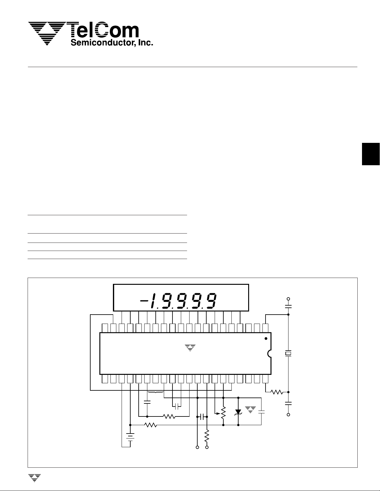
TYPICAL OPERATING CIRCUIT
LOW BATTERY CONTINUITY
GENERAL DESCRIPTION
The TC7129 is a 4-1/2 digit analog-to-digital converter
(ADC) that directly drives a multiplexed liquid crystal display (LCD). Fabricated in high-performance, low-power
CMOS, the TC7129 ADC is designed specifically for highresolution, battery-powered digital multimeter applications.
The traditional dual-slope method of A/D conversion has
been enhanced with a successive integration technique to
produce readings accurate to better than 0.005% of full
scale, and resolution down to 10 µV per count.
The TC7129 includes features important to multimeter
applications. It detects and indicates low-battery condition.
A continuity output drives an annunciator on the display, and
can be used with an external driver to sound an audible
alarm. Overrange and underrange outputs and a rangechange input provide the ability to create auto-ranging
instruments. For snapshot readings, the TC7129 includes a
latch-and-hold input to freeze the present reading. This
combination of features makes the TC7129 the ideal
choice for full-featured multimeter and digital measurement
applications.
+
V
3
4
5
20
+
9V
NOTE:
*
TELCOM SEMICONDUCTOR, INC.
9
1011
12
13141516171819
TC7129
29
27262524232221
28
*
0.1 µF
1 µF
150 kΩ
10 kΩ
RC network between pins 26 and 28 is not required.
8
323130
33
0.1
+
µF
100 kΩ
–
V
IN
567
3534
36
20
kΩ
+
3837
TC04
5 pF
1234
6
120 kHz
39
40
330 kΩ
7
0.1 µF
V
10 pF
+
8
TC7129-5 10/18/96
3-231
TC7129
4-1/2 DIGIT ANALOG-TO-DIGITAL
CONVERTER WITH ON-CHIP LCD DRIVERS
ABSOLUTE MAXIMUM RATINGS*
Supply Voltage (V+ to V–)............................................15V
Reference Voltage (REF HI or REF LO) .............. V+ to V
Input Voltage (IN HI or IN LO) (Note 1)................ V+ to V
V
................................................V+ to (DGND – 0.3V)
DISP
Digital Input, Pins
1, 2, 19, 20, 21, 22, 27, 37, 39, 40.......... DGND to V
Analog Input, Pins 25, 29, 30 ............................... V+ to V
Package Power Dissipation (TA ≤ 70°C)
Plastic DIP ........................................................1.23W
PLCC ................................................................1.23W
Plastic QFP.......................................................1.00W
Operating Temperature Range .................... 0°C to +70°C
ELECTRICAL CHARACTERISTICS: V
+
to V– = 9V, V
Storage Temperature Range ................– 65°C to +150°C
Lead Temperature (Soldering, 10 sec) .................+300°C
–
Notes: Input voltages may exceed supply voltages, provided input current
is limited to ±400 µA. Currents above this value may result in invalid display
–
readings but will not destroy the device if limited to ±1 mA.
Dissipation ratings assume device is mounted with all leads soldered to
printed circuit board.
+
–
*Static-sensitive device. Unused devices must be stored in conductive
material. Protect devices from static discharge and static fields. Stresses
above those listed under Absolute Maximum Ratings may cause permanent damage to the device. These are stress ratings only and functional
operation of the device at these or any other conditions above those
indicated in the operational sections of the specifications is not implied.
Exposure to Absolute Maximum Rating Conditions for extended periods
may affect device reliability.
= 1V, TA = +25°C, f
REF
= 120 kHz, unless otherwise
CLK
indicated. Pin numbers refer to 40-pin DIP.
Symbol Parameter Test Conditions Min Typ Max Unit
Input
Zero Input Reading VIN = 0V, 200 mV Scale – 0000 0000 +0000 Counts
Zero Reading Drift VIN = 0V, 0°C < TA < +70°C—±0.5 — µV/°C
Ratiometric Reading VIN = V
Range Change Accuracy V
= 0.1V on Low Range 0.9999 1.0000 1.0001 Ratio
IN
4VIN = 1V on High Range
RE Roll-Over Error –VIN = +VIN = 199 mV — 1 2 Counts
NL Linearity Error 200 mV Scale — 1 — Counts
CMRR Common-Mode Rejection Ratio VCM = 1V, VIN = 0V, 200 mV Scale — 110 — dB
CMVR Common-Mode Voltage Range V
= 0V — (V–) +1.5 — V
IN
200 mV Scale — (V+) –1 — V
e
N
Noise (Peak-to-Peak Value Not VIN = 0V — 14 — µV
Exceeded 95% of Time) 200 mV Scale
I
IN
Input Leakage Current VIN = 0V, Pins 32, 33 — 1 10 pA
Scale Factor Temperature V
= 199 mV, 0°C < TA < +70°C — 2 7 ppm/°C
IN
Coefficient External V
Power
V
COM
Common Voltage V+ to Pin 28 2.8 3.2 3.5 V
Common Sink Current ∆ Common = +0.1V — 0.6 — mA
Common Source Current ∆Common = –0.1V — 10 — µA
DGND Digital Ground Voltage V+ to Pin 36, V+ to V– = 9V 4.5 5.3 5.8 V
Sink Current ∆DGND = +0.5V — 1.2 — mA
Supply Voltage Range V+ to V
I
S
f
CLK
Supply Current Excluding Common Current V+ to V– = 9V — 0.8 1.3 mA
Clock Frequency — 120 360 kHz
V
Resistance V
DISP
DISP
Low-Battery Flag Activation Voltage V+ to V
Digital
Continuity Comparator V
Threshold Voltages V
OUT
OUT
Pull-Down Current Pins 37, 38, 39 — 2 10 µA
= 1000 mV, Range = 2V 9997 9999 10000 Counts
REF
P-P
= 0 ppm/°C
REF
–
to V
–
+
6912V
—50 —kΩ
6.3 7.2 7.7 V
Pin 27 = High 100 200 — mV
Pin 27 = Low — 200 400 mV
3-232
TELCOM SEMICONDUCTOR, INC.
4-1/2 DIGIT ANALOG-TO-DIGITAL
CONVERTER WITH ON-CHIP LCD DRIVERS
1
TC7129
ELECTRICAL CHARACTERISTICS: V
+
to V– = 9V, V
= 1V, TA = +25°C, f
REF
= 120 kHz, unless otherwise
CLK
indicated. Pin numbers refer to 40-pin DIP.
Symbol Parameter Test Conditions Min Typ Max Unit
"Weak Output" Current Pins 20, 21 Sink/Source — 3/3 — µA
Sink/Source Pin 27 Sink/Source — 3/9 — µA
Pin 22 Source Current — 40 — µA
Pin 22 Sink Current — 3 — µA
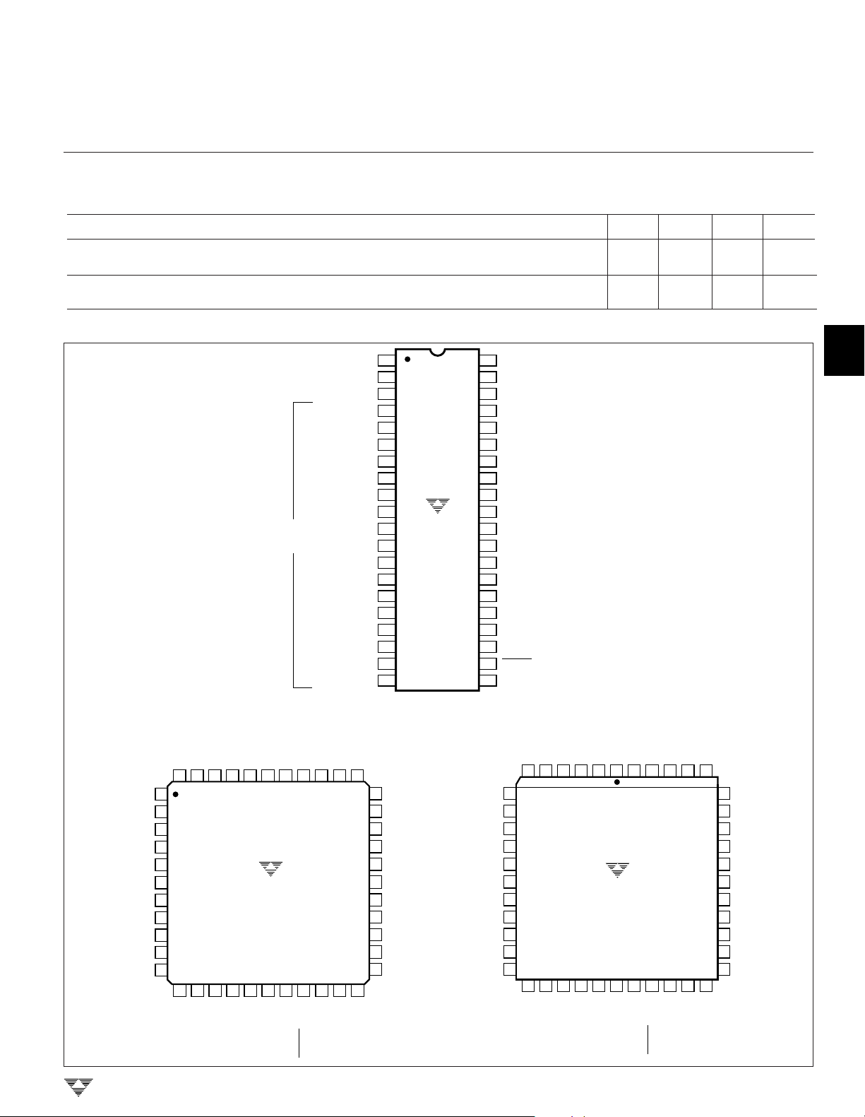
PIN CONFIGURATIONS
40
40-Pin PDIP
OSC
OSC
ANNUNICATOR DRIVE
B1, C1, CONT
A1, G1, D
F1, E1, DP
B2, C2, LO BATT
A2, G2, D
F2, E2, DP
B3, C
MINUS
DISPLAY
OUTPUT
LINES
3,
A3, G3, D
F3, E3, DP
B4, C
4, BC5
A4, G4, D
F4, E4, DP
V
DISP
DP4/OR
BP
BP
BP
1
1
2
3
3
4
5
1
6
1
7
8
2
9
2
10
TC7129CPL
11
3
12
3
13
14
4
15
4
16
3
17
2
18
1
19
20
OSC
DP
39
38
DP
37
RANGE
36
DGND
REF LO
35
REF HI
34
IN HI
33
32
IN LO
31
BUFF
C
30
29
C
28
COM
CONT
27
INT OUT
26
INT IN
25
V
24
23
V
22
LATCH/HOLD
21
DP3/UR
1
2
–
REF
+
REF
+
–
2
2
3
4
5
44-Pin QFP
, CONT
1
, C
1
B
A.D.
1
2
BP
OSC3OSC1NC
TC7129CKW
16
NC
/OR
4
DISP
V
DP
OSC2DP1DP2RANGE
/UR
3
DP
F1, E1, DP
B2, C2, BATT
A2, G2, D
F2, E2, DP
B3, C
MINUS
3,
A3, G3, D
F3, E3, DP
B4, C
4, BC5
A4, G4, D
F4, E4, DP
1
, D
1
, G
1
A
44 43 42 41 39 3840
1
1
2
3
2
4
2
5
NC
6
7
3
8
3
9
10
4
11
4
12 13 14 15 17 18
BP3BP
TELCOM SEMICONDUCTOR, INC.
37 36 35 34
19 20 21 22
–
V+V
LATCH/HOLD
DGND
33
32
31
30
29
28
27
26
25
24
23
INT IN
REF LO
REF HI
IN HI
IN LO
BUFF
NC
–
C
REF
+
C
REF
COM
CONT
INT OUT
F1, E1, DP
B2, C2, BATT
A2, G2, D
F2, E2, DP
B3, C
MINUS
3,
A3, G3, D
F3, E3, DP
B4, C
4, BC5
A4, G4, D
F4, E4, DP
1
, D
, CONT
1
1
, G
, C
1
1
A
B
6543 1442
7
1
8
9
2
10
2
11
12
NC
13
3
3
4
4
18 19 20 21 23 24
2
BP3BP
44-Pin PLCC
A.D.
OSC3OSC1NC
TC7129CLW
22
1
BP
DISP
V
/OR
4
DP
NC
OSC2DP1DP2RANGE
43 42 41 40
25 26 27 28
/UR
3
DP
LATCH/HOLD
DGND
–
V+V
INT IN
39
38
37
36
35
34
33
3214
3115
3016
2917
REF LO
REF HI
IN HI
IN LO
BUFF
NC
–
C
REF
+
C
REF
COM
CONT
INT OUT
6
7
8
3-233
4-1/2 DIGIT ANALOG-TO-DIGITAL
CONVERTER WITH ON-CHIP LCD DRIVERS
TC7129
PIN DESCRIPTIONS
Pin No. Pin No. Pin No.
40-Pin 44-Pin 44-Pin
TC7129CPL TC7129CKW TC7129CLW Symbol Function
1 40 2 OSC
2 41 3 OSC
1
3
3 ANNUNCIATOR Backplane square-wave output for driving annunciators.
4435B
5446A
617F
728B
839A
9410F
, C1, CONT Output to display segments.
1
, G1, D
1
1
, C2, LO BATT Output to display segments.
2
2
2
, E1, DP
, G2, D
, E2, DP
1
1
2
2
10 5 11 B3, C3, MINUS Output to display segments.
11 7 13 A3, G3, D
12 8 14 F3, E3, DP
13 9 15 B4, C4, BC
14 10 16 A4, D4, G
15 11 17 F4, E4, DP
16 12 18 BP
17 13 19 BP
18 14 20 BP
19 15 21 V
20 16 22 DP
21 18 24 DP
3
3
5
4
4
3
2
1
DISP
/OR Input: When HI, turns on most significant decimal point.
4
/UR Input: Second most significant decimal point on when HI.
3
22 19 25 LATCH/HOLD Input: When floating, ADC operates in the free-run mode.
23 20 26 V
24 27 V
–
+
25 21 28 INT IN Input to integrator amplifier.
26 23 29 INT OUT Output of integrator amplifier.
27 24 30 CONTINUITY Input: When LO, continuity flag on the display is OFF.
28 25 31 COMMON Sets common-mode voltage of 3.2V below V
29 26 32 C
30 27 33 C
+
REF
–
REF
31 29 35 BUFFER Output of buffer amplifier.
32 30 36 IN LO Negative input voltage terminal.
33 31 37 IN HI Positive input voltage terminal.
Input to first clock inverter.
Output of second clock inverter.
Output to display segments.
Output to display segments.
Output to display segments.
Output to display segments.
Output to display segments.
Output to display segments.
Output to display segments.
Output to display segments.
Output to display segments.
Backplane #3 output to display.
Backplane #2 output to display.
Backplane #1 output to display.
Negative rail for display drivers.
Output: Pulled HI when result count exceeds ±19,999.
Output: Pulled HI when result count is less than ±1000.
When pulled HI, the last displayed reading is held. When
pulled LO, the result counter contents aren shown
inincrementing during the deintegrate phase of cycle.
Output: Negative-going edge occurs when the data latches
are updated. Can be used for converter status signal.
Negative power supply terminal.
Positive power supply terminal and positive rail for display
drivers.
When HI, continuity flag is ON.
Output: HI when voltage between inputs is less than +200
mV. LO when voltage between inputs is more than +200
mV.
10X, etc. Can be used as preregulator for external
reference.
Positive side of external reference capacitor.
Negative side of external reference capacitor.
+
for DE,
3-234
TELCOM SEMICONDUCTOR, INC.
4-1/2 DIGIT ANALOG-TO-DIGITAL
CONVERTER WITH ON-CHIP LCD DRIVERS
PIN DESCRIPTIONS
1
TC7129
Pin No. Pin No. Pin No.
40-Pin 44-Pin 44-Pin
TC7129CPL TC7129CKW TC7129CLW Symbol Function
34 32 38 REF HI Positive reference voltage in
35 33 39 REF LO Negative reference voltage
36 34 40 DGND Internal ground reference for digital section. See "±5V Power
Supply" paragraph.
37 35 41 RANGE 3 µA pull-down for 200 mV scale. Pulled HI externally for 2V
scale.
38 36 42 DP
39 37 43 DP
40 38 44 OSC
6,17, 28, 39 12, 23, 34,1 NC No Connection
2
1
2
Internal 3 µA pull-down. When HI, decimal point 2 will be on.
Internal 3 µA pull-down. When HI, decimal point 1 will be on.
Output of first clock inverter. Input of second clock inverter.
COMPONENT SELECTION
(All pin designations refer to 40-Pin Dip)
The TC7129 is designed to be the heart of a highresolution analog measurement instrument. The only additional components required are a few passive elements, a
voltage reference, an LCD, and a power source. Most
component values are not critical; substitutes can be chosen
based on the information given below.
The basic circuit for a digital multimeter application is
shown in Figure 1. See "Special Applications" for variations.
Typical values for each component are shown. The sections
below give component selection criteria.
Oscillator (X
The primary criterion for selecting the crystal oscillator
is to chose a frequency that achieves maximum rejection of
line-frequency noise. To do this, the integration phase
should last an integral number of line cycles. The integration
phase of the TC7129 is 10,000 clock cycles on the 200 mV
range and 1000 clock cycles on the 2V range. One clock
cycle is equal to two oscillator cycles. For 60 Hz rejection, the
oscillator frequency should be chosen so that the period of
one line cycle equals the integration time for the 2V range:
1/60 second = 16.7 msec =
1000 clock cycles 2 osc cycles/clock cycle
, CO1, CO2, RO)
OSC
*
oscillator frequency
,
The resistor and capacitor values are not critical; those
shown work for most applications. In some situations, the
capacitor values may have to be adjusted to compensate for
parasitic capacitance in the circuit. The capacitors can be
low-cost ceramic devices.
Some applications can use a simple RC network instead
of a crystal oscillator. The RC oscillator has more potential
for jitter, especially in the least significant digit. See "RC
Oscillator."
Integrating Resistor (R
The integrating resistor sets the charging current for
the integrating capacitor. Choose a value that provides a
current between 5 µA and 20 µA at 2V, the maximum fullscale input. The typical value chosen gives a charging
current of 13.3 µA:
I
CHARGE
Too high a value for R
noise pickup and increases errors due to leakage current.
Too low a value degrades the linearity of the integration,
leading to inaccurate readings.
2V
= 13.3 µA
150 kΩ
)
INT
increases the sensitivity to
INT
2
3
4
5
6
7
giving an oscillator frequency of 120 kHz. A similar calculation gives an optimum frequency of 100 kHz for 50 Hz
rejection.
TELCOM SEMICONDUCTOR, INC.
8
3-235

TC7129
4-1/2 DIGIT ANALOG-TO-DIGITAL
CONVERTER WITH ON-CHIP LCD DRIVERS
LOW BATTERY CONTINUITY
+
V
20
DP
4
/OR
DP
3
/UR
V
DISP
LATCH/
HOLD
5 pF
OSC
3
DP
1
39
1234567
OSC
1
120
kHz
OSC
2
40
9
12
13141516171819
1011
8
ANNUNC
DISPLAY DRIVE OUTPUTS
CONTINUITY
27262524232221
COMMON
C
REF
+
29
28
INT OUT
INT IN
V
V
+
–
C
REF
–
BUFFER
TC7129
IN LO
323130
IN HI
33
REF LO
REF HI
3534
DGND
36
RANGE
DP
2
3837
C
O1
CRYSTAL
330 kΩ
C
RF
0.1 µF
R
O
10 pF
C
O2
+
V
C
INT
0.1
µF
C
1 µf
150 kΩ
R
INT
REF
+
0.1
µF
R
REF
20
D
REF
kΩ
C
IF
TC04
3-236
9V
10 kΩ
R
BIAS
R
IF
100 kΩ
+
– +
V
IN
Figure 1. Standard Circuit
TELCOM SEMICONDUCTOR, INC.

4-1/2 DIGIT ANALOG-TO-DIGITAL
CONVERTER WITH ON-CHIP LCD DRIVERS
1
TC7129
Integrating Capacitor (C
The charge stored in the integrating capacitor during
the integrate phase is directly proportional to the input
voltage. The primary selection criterion for C
a value that gives the highest voltage swing while remaining within the high-linearity portion of the integrator output
range. An integrator swing of 2V is the recommended
value. The capacitor value can be calculated from the
equation:
t
x I
INT
C
= ,
INT
where t
operation), the equation becomes:
ensure good integration linearity. Polypropylene and Teflon
capacitors are usually suitable. A good measurement of the
dielectric absorption is to connect the reference capacitor
across the inputs by connecting:
is the integration time.
INT
Using the values derived above (assuming 60 Hz
C
The capacitor should have low dielectric absorption to
16.7msec x 13.3 µA
= = 0.1 µF.
INT
V
SWING
INT
2V
INT
)
is to choose
INT
Voltage Reference (D
A TC04 band-gap reference provides a high-stability
voltage reference of 1.25V. The reference potentiometer
(R
) provides an adjustment for adjusting the reference
REF
voltage; any value above 20 kΩ is adequate. The bias
resistor (R
150 µA. The reference filter capacitor (CRF) forms an RC
filter with R
) limits the current through D
BIAS
to help eliminate noise.
BIAS
REF
, R
REF
, R
, CRF)
BIAS
to less than
REF
Input filter (RIF, CIF)
For added stability, an RC input noise filter is usually
included in the circuit. The input filter resistor value should
not exceed 100 kΩ. A typical RC time constant value is
16.7msec to help reject line-frequency noise. The input filter
capacitor should have low leakage for a high-impedance
input.
Battery
The typical circuit uses a 9V battery as a power source.
Any value between 6V and 12V can be used. For operation
from batteries with voltages lower than 6V and for operation
from power supplies, see "Powering the TC7129."
SPECIAL APPLICATIONS
2
3
4
Pin to Pin
20 → 33 (C
30 → 32 (C
A reading between 10,000 and 9998 is acceptable;
anything lower indicates unacceptably high dielectric absorption.
Reference Capacitor (C
The reference capacitor stores the reference voltage
during several phases of the measurement cycle. Low
leakage is the primary selection criterion for this component.
The value must be high enough to offset the effect of stray
capacitance at the capacitor terminals. A value of at least
1 µF is recommended.
REF
REF
+
–
to IN HI)
to IN LO)
REF
)
The TC7129 as a Replacement Part
The TC7129 is a direct pin-for-pin replacement part for
the ICL7129. Note, however, that part requires a capacitor
and resistor between pins 26 and 28 for phase compensation. Since the TC7129 uses internal phase compensation,
these parts are not required and, in fact, must be removed
from the circuit for stable operation.
Powering the TC7129
While the most common power source for the TC7129
is a 9V battery, there are other possibilities. Some of the
more common ones are explained below.
5
6
7
TELCOM SEMICONDUCTOR, INC.
8
3-237

TC7129
±5V Power Supply
4-1/2 DIGIT ANALOG-TO-DIGITAL
CONVERTER WITH ON-CHIP LCD DRIVERS
Measurements are made with respect to power supply
ground. DGND (pin 36) is set internally to about 5V less than
V+ (pin 24); it is not intended as a power supply input and
must not be tied directly to power supply ground. (It can be
used as a reference for external logic, as explained in
"Connecting to External Logic." (See Figure 2.)
+5V
24
+
0.1 µF
0.1 µF
0.1 µF
36
V
REF HI
REF LO
DGND
TC7129
V
23
COM
IN HI
IN LO
–
34
35
28
33
32
TC04
V
IN
+
–
24
+
V
36
+
3.8V
TO
6V
REF HI
DGND
REF LO
TC7129
8
TC7660
3
2
+
4
5
10 µF
10 µF
–
V
COM
IN HI
IN LO
23
34
TC04
35
28
33
32
+
Figure 3. Powering the TC7129 From a Low-Voltage Battery
+
5V
+
V
IN
–
–5V
Figure 2. Powering the TC7129 From a ±5V Power Supply
Low-Voltage Battery Source
A battery with voltage between 3.8V and 6V can be used
to power the TC7129 when used with a voltage-doubler
circuit as shown in Figure 3. The voltage doubler uses the
TC7660 DC-to-DC voltage converter and two external capacitors.
+5V Power Supply
Measurements are made with respect to power supply
ground. COMMON (pin 28) is connected to REF LO (pin 35).
A voltage doubler is needed, since the supply voltage is less
than the 6V minimum needed by the TC7129. DGND (pin
36) must be isolated from power supply ground.
(See Figure 4.)
Connecting to External Logic
External logic can be directly referenced to DGND (pin
36), provided that the supply current of the external logic
does not exceed the sink current of DGND (Figure 5). A safe
value for DGND sink current is 1.2 mA. If the sink current is
expected to exceed this value, a buffer is recommended.
(See Figure 6.)
24
+
8
+
V
TC7660
GND
3
0.1 µF
0.1 µF
2
4
5
10 µF
V
36
DGND
TC7129
V
+
10 µF
34
TC04
35
28
33
32
–
23
+
Figure 4. Powering the TC7129 From a +5V Power Supply
+
V
IN
–
3-238
TELCOM SEMICONDUCTOR, INC.

4-1/2 DIGIT ANALOG-TO-DIGITAL
CONVERTER WITH ON-CHIP LCD DRIVERS
1
TC7129
+
V
24
EXTERNAL
LOGIC
TC7129
36
DGND
I
LOGIC
23
–
V
Figure 5. External Logic Referenced Directly to DGND Figure 6. External Logic Referenced to DGND With Buffer
EXTERNAL
LOGIC
I
LOGIC
–
36
+
TC7129
DGND
+
V
24
23
–
V
Temperature Compensation
For most applications, V
directly to DGND (pin 36). For applications with a wide
temperature range, some LCDs require that the drive levels
vary with temperature to maintain good viewing angle and
display contrast. Figure 7 shows two circuits that can be
(pin 19) can be connected
DISP
adjusted to give temperature compensation of about 10
mV/°C between V+ (pin 24) and V
DGND and V
cause V
DISP
should have a low turn-ON voltage be-
DISP
cannot exceed 0.3V below DGND.
. The diode between
DISP
2
3
4
5
1N4148
5 kΩ
75 kΩ
39 kΩ
–
+
200 kΩ
+
V
24
20 kΩ
TC7129
19
V
DISP
36
DGND
23
–
V
Figure 7. Temperature Compensating Circuits
39 kΩ
2N2222
18 kΩ
19
36
TC7129
V
DISP
DGND
+
V
24
6
7
23
–
V
8
TELCOM SEMICONDUCTOR, INC.
3-239

TC7129
4-1/2 DIGIT ANALOG-TO-DIGITAL
CONVERTER WITH ON-CHIP LCD DRIVERS
RC Oscillator
For applications in which 3-1/2 digit (100 µV) resolution
is sufficient, an RC oscillator is adequate. A recommended
value for the capacitor is 51 pF. Other values can be used as
long as they are sufficiently larger than the circuit parasitic
capacitance. The resistor value is calculated from:
0.45
R =
freq C
*
For 120 kHz frequency and C = 51 pF, the calculated
value of R is 75 kΩ. The RC oscillator and the crystal
oscillator circuits are shown in Figure 8.
Measuring Techniques
Two important techniques are used in the TC7129:
successive integration and digital auto-zeroing. Successive
integration is a refinement to the traditional dual-slope
conversion technique.
Dual-Slope Conversion
A dual-slope conversion has two basic phases: integrate and deintegrate. During the integrate phase, the input
signal is integrated for a fixed period of time; the integrated
voltage level is thus proportional to the input voltage. During
the deintegrate phase, the integrated voltage is ramped
down at a fixed slope, and a counter counts the clock cycles
until the integrator voltage crosses zero. The count is a
measurement of the time to ramp the integrated voltage to
zero, and is therefore proportional to the input voltage being
measured. This count can then be scaled and displayed as
a measurement of the input voltage. Figure 9 shows the
phases of the dual-slope conversion.
The dual-slope method has a fundamental limitation.
The count can only stop on a clock cycle, so that measurement accuracy is limited to the clock frequency. In addition,
a delay in the zero-crossing comparator can add to the
inaccuracy. Figure 10 shows these errors in an actual
measurement.
INTEGRATE
TIME
Figure 9. Dual-Slope Conversion
DEINTEGRATE
ZERO
CROSSING
Successive Integration
The successive integration technique picks up where
dual-slope conversion ends. The overshoot voltage shown
in Figure 10, called the "integrator residue voltage," is
measured to obtain a correction to the initial count. Figure 11
shows the cycles in a successive integration measurement.
The waveform shown is for a negative input signal. The
sequence of events during the measurement cycle is:
+
V
3-240
1 40 2
270 kΩ
5 pF
120 kHz
1 40 2
Figure 8. Oscillator Circuits
10 pF
75 kΩ
51 pF
V
+
TC7129
TC7129
Phase Description
INT
1
DE
1
REST Rest; circuit settles.
X10 Residue voltage is amplified 10 times and inverted.
DE
2
REST Rest; circuit settles.
X10 Residue voltage is amplified 10 times and inverted.
DE
3
Input signal is integrated for fixed time. (1000 clock
cycles on 2V scale, 10,000 on 200 mV)
Integrator voltage is ramped to zero. Counter counts
up until zero crossing to produce reading accurate
to 3-1/2 digits. Residue represents an overshoot of
the actual input voltage.
Integrator voltage is ramped to zero. Counter counts
down until zero crossing to correct reading to 4-1/2
digits. Residue represents an undershoot of the
actual input voltage.
Integrator voltage is ramped to zero. Counter counts
up until zero crossing to correct reading to 5-1/2
digits. Residue is discarded.
TELCOM SEMICONDUCTOR, INC.

4-1/2 DIGIT ANALOG-TO-DIGITAL
CONVERTER WITH ON-CHIP LCD DRIVERS
1
TC7129
ZERO
INTEGRATE
AND LATCH
TIME
INTEGRATE
INT
1
INTEGRATE
DEINTEGRATE
OVERSHOOT DUE TO ZERO CROSSING
BETWEEN CLOCK PULSES
INTEGRATOR RESIDUE VOLTAGE
OVERSHOOT CAUSED BY
COMPARATOR DELAY OF
CLOCK PULSES
Figure 10. Accuracy Errors in Dual-Slope Conversion
DE
DEINTEGRATE
1
REST X10
1 CLOCK PULSE
REST
DE
2
X10
DE
ZERO INTEGRATE
3
2
3
4
NOTE:
Digital Auto-Zeroing
To eliminate the effect of amplifier offset errors, the
TC7129 uses a digital auto-zeroing technique. After the
input voltage is measured as described above, the measurement is repeated with the inputs shorted internally. The
reading with inputs shorted is a measurement of the internal
errors and is subtracted from the previous reading to obtain
a corrected measurement. Digital auto-zeroing eliminates
the need for an external auto-zeroing capacitor used in other
ADCs.
Shaded area greatly expanded
in time and amplitude.
INTEGRATOR
Figure 11. Integrator Waveform
TC7129
RESIDUAL VOLTAGE
Inside the TC7129
Figure 12 shows a simplified block diagram of the
TC7129.
Integrator Section
The integrator section includes the integrator, comparator, input buffer amplifier, and analog switches used to
change the circuit configuration during the separate measurement phases described earlier.
5
6
7
8
TELCOM SEMICONDUCTOR, INC.
3-241

TC7129
OSC
4-1/2 DIGIT ANALOG-TO-DIGITAL
CONVERTER WITH ON-CHIP LCD DRIVERS
LOW BATTERY CONTINUITY
BACKPLANE
SEGMENT DRIVES
1
DRIVES
ANNUNCIATOR
DRIVE
OSC
OSC
RANGE
L/H
CONT
V
V
DGND
LATCH, DECODE DISPLAY MULTIPLEXER
2
UP/DOWN RESULTS COUNTER
3
SEQUENCE COUNTER/DECODER
CONTROL LOGIC
+
–
ANALOG SECTION
V
DISP
DP
1
DP
2
UR/DP
OR/DP
REF HI
REF LO
3
4
3-242
TC7129
COMMON INHIIN
LO
Figure 12. Functional Block Diagram
INT OUT
INT IN
BUFF
TELCOM SEMICONDUCTOR, INC.

4-1/2 DIGIT ANALOG-TO-DIGITAL
CONVERTER WITH ON-CHIP LCD DRIVERS
1
TC7129
C
REF
REF HI
DE
INT
IN HI
COMMON
IN LO
CONTINUITY
Table I. Switch Legends
Label Meaning
DE Open during all deintegrate phases.
DE– Closed during all deintegrate phases when input
voltage is negative.
DE+ Closed during all deintegrate phases when input
voltage is positive.
INT
1
INT
2
INT Open during both integrate phases.
REST Closed during the rest phase.
ZI Closed during the zero-integrate phase.
X10 Closed during the X10 phase.
X10 Open during the X10 phase.
The buffer amplifier has a common-mode input voltage
range from 1.5V above V– to 1V below V+. The integrator
amplifier can swing to within 0.3V of the rails, although for
best linearity the swing is usually limited to within 1V. Both
amplifiers can supply up to 80 µA of output current, but
should be limited to 20 µA for good linearity.
Closed during the first integrate phase
(measurement of the input voltage).
Closed during the second integrate phase
(measurement of the amplifier offset).
1
INT1, INT
–
V
200 mV
DE– DE+
DE+
2
+
REF LO
DE
DE–
INT
–
+
CONTINUITY
COMPARATOR
–
+
BUFFER
ZI, X10
REST
500 kΩ
Figure 13. Integrator Block Diagram
Continuity Indicator
A comparator with a 200 mV threshold is connected
between IN HI (pin 33) and IN LO (pin 32). Whenever the
voltage between inputs is less than 200 mV, the
R
INT
C
INT
INTEGRATOR
–
+
100 pF
TC7129
IN HI
COM
IN LO
200 mV
CONT
Figure 14. Continuity Indicator Circuit
CONTINUITY output (pin 27) will be pulled HIGH, activating
the continuity annunciator on the display. The continuity
pin can also be used as an input to drive the continuity
annunciator directly from an external source. A schematic
of the input/output nature of this pin is shown in Figure 15.
X10
10
COMPARATOR 1
pF
TO DISPLAY DRIVER
V
+
–
–
+
500 kΩ
TO DIGITAL
SECTION
COMPARATOR 2
–
+
TC7129
TO DISPLAY
DRIVER
(NOT LATCHED)
2
3
4
5
BUFFER
6
7
8
TELCOM SEMICONDUCTOR, INC.
3-243

CONVERTER WITH ON-CHIP LCD DRIVERS
TC7129
TC7129
DP4/OR, PIN 20
DP3/UR, PIN 21
LATCH/HOLD PIN 22
CONTINUITY, PIN 27
Figure 15. Input/Output Pin Schematic
Common and Digital Ground
The common and digital ground (DGND) outputs are
generated from internal zener diodes. The voltage between
V+ and DGND is the internal supply voltage for the digital
section of the TC7129. Common can source approximately
12 µA; DGND has essentially no source capability.
'500 kΩ
4-1/2 DIGIT ANALOG-TO-DIGITAL
Sequence and Results Counter
A sequence counter and associated control logic provide signals that operate the analog switches in the integrator section. The comparator output from the integrator gates
the results counter. The results counter is a six-section up/
down decade counter which holds the intermediate results
from each successive integration.
Overrange and Underrange Outputs
When the results counter holds a value greater than
±19,999, the DP4/OR output (pin 20) is driven HIGH. When
the results counter value is less than ±1000, the DP3/UR
output (pin 21) is driven HIGH. Both signals are valid on the
falling edge of LATCH/HOLD (L/H) and do not change until
the end of the next conversion cycle. The signals are
updated at the end of each conversion unless the L/H input
(pin 22) is held HIGH. Pins 20 and 21 can also be used as
inputs for external control of decimal points 3 and 4. Figure
15 shows a schematic of the input/output nature of these
pins.
Low Battery
The low battery annunciator turns on when supply
voltage between V+ and V– drops below 6.8V. The internal
zener has a threshold of 6.3V. When the supply voltage
drops below 6.8V, the transistor tied to V– turns OFF, pulling
the "Low Battery" point HIGH. (See Figure 16.)
24
+
V
12 µA
–
+
TC7129
Figure 16. Digital Ground (DGND) and Common Outputs
N
LOGIC
SECTION
P
N
5V
3.2V
28
36
23
COM
DGND
–
V
Latch/Hold
The L/H output goes LOW during the last 100 cycles of
each conversion. This pulse latches the conversion data into
the display driver section of the TC7129. This pin can also
be used as an input. When driven HIGH, the display will not
be updated; the previous reading is displayed. When driven
LOW, the display reading is not latched; the sequence
counter reading will be displayed. Since the counter is
counting much faster than the backplanes are being updated, the reading shown in this mode is somewhat erratic.
Display Driver
The TC7129 drives a triplexed LCD with three backplanes. The LCD can include decimal points, polarity sign,
and annunciators for continuity and low battery. Figure 17
shows the assignment of the display segments to the
backplanes and segment drive lines. The backplane drive
frequency is obtained by dividing the oscillator frequency by
1200. This results in a backplane drive frequency of 100 Hz
for 60 Hz operation (120 kHz crystal) and 83.3 Hz for 50 Hz
operation (100 kHz crystal).
Backplane waveforms are shown in Figure 18. These
appear on outputs BP1, BP2, BP3 (pins 16, 17, and 18). They
remain the same regardless of the segments being driven.
Other display output lines (pins 4 through 15) have
waveforms that vary depending on the displayed values.
Figure 19 shows a set of waveforms for the A, G, D outputs
(pins 5, 8, 11, and 14) for several combinations of "ON"
segments.
3-244
TELCOM SEMICONDUCTOR, INC.

V
DD
V
H
V
L
V
DISP
V
DD
V
H
V
L
V
DISP
V
DD
V
H
V
L
V
DISP
V
DD
V
H
V
L
V
DISP
b SEGMENT
LINE
ALL OFF
a SEGMENT
ON
d, g OFF
a, g ON
d OFF
ALL ON
4-1/2 DIGIT ANALOG-TO-DIGITAL
CONVERTER WITH ON-CHIP LCD DRIVERS
1
TC7129
F4, E4, DP
A4, G4, D
B4, C4, BC
F3, E3, DP
A3, G3, D
B3, C3, MINUS
LOW BATTERY
CONTINUITY
2
BP
1
BP
BP
LOW BATTERY CONTINUITY
BACKPLANE
2
CONNECTIONS
3
3
4
4
4
4
3
3
B1, C1, CONTINUITY
A1, G1, D
F1, E1, DP
B2, C2, LOW BATTERY
A2, G2, D
F2, E2, DP
1
1
2
2
Figure 17. Display Segment Assignments
BP
1
BP
2
BP
3
Figure 18. Backplane Waveforms
The ANNUNCIATOR DRIVE output (pin 3) is a squarewave running at the backplane frequency (100 Hz or 83.3 Hz),
with a peak-to-peak voltage equal to DGND voltage. Connecting an annunciator to pin 3 turns it ON; connecting it to
its backplane turns it OFF.
TELCOM SEMICONDUCTOR, INC.
Figure 19. Typical Display Output Waveforms
5
6
7
8
3-245
 Loading...