

TelCom Semiconductor Inc TC7126ARCPL, TC7126ARCLW, TC7126ARCKW, TC7126ACPL, TC7126RIPL Datasheet
...
3-217
TELCOM SEMICONDUCTOR, INC.
7
6
5
4
3
1
2
8
TC7126
TC7126A
3-1/2 DIGIT ANALOG-TO-DIGITAL CONVERTERS
FEATURES
■ Low Temperature Drift Internal Reference
TC7126 ....................................... 80 ppm/°C Typ
TC7126A.....................................35 ppm/°C Typ
■ Guaranteed Zero Reading With Zero Input
■ Low Noise....................................................15 µV
P-P
■ High Resolution .............................................. 0.05%
■ Low Input Leakage Current ......................1 pA Typ
10 pA Max
■ Precision Null Detectors With True Polarity at
Zero
■ High-Impedance Differential Input
■ Convenient 9V Battery Operation With
Low Power Dissipation ........................500 µW Typ
900 µW Max
TYPICAL APPLICATIONS
■ Thermometry
■ Bridge Readouts: Strain Gauges, Load Cells, Null
Detectors
■ Digital Meters and Panel Meters
— Voltage/Current/Ohms/Power, pH
■ Digital Scales, Process Monitors
GENERAL DESCRIPTION
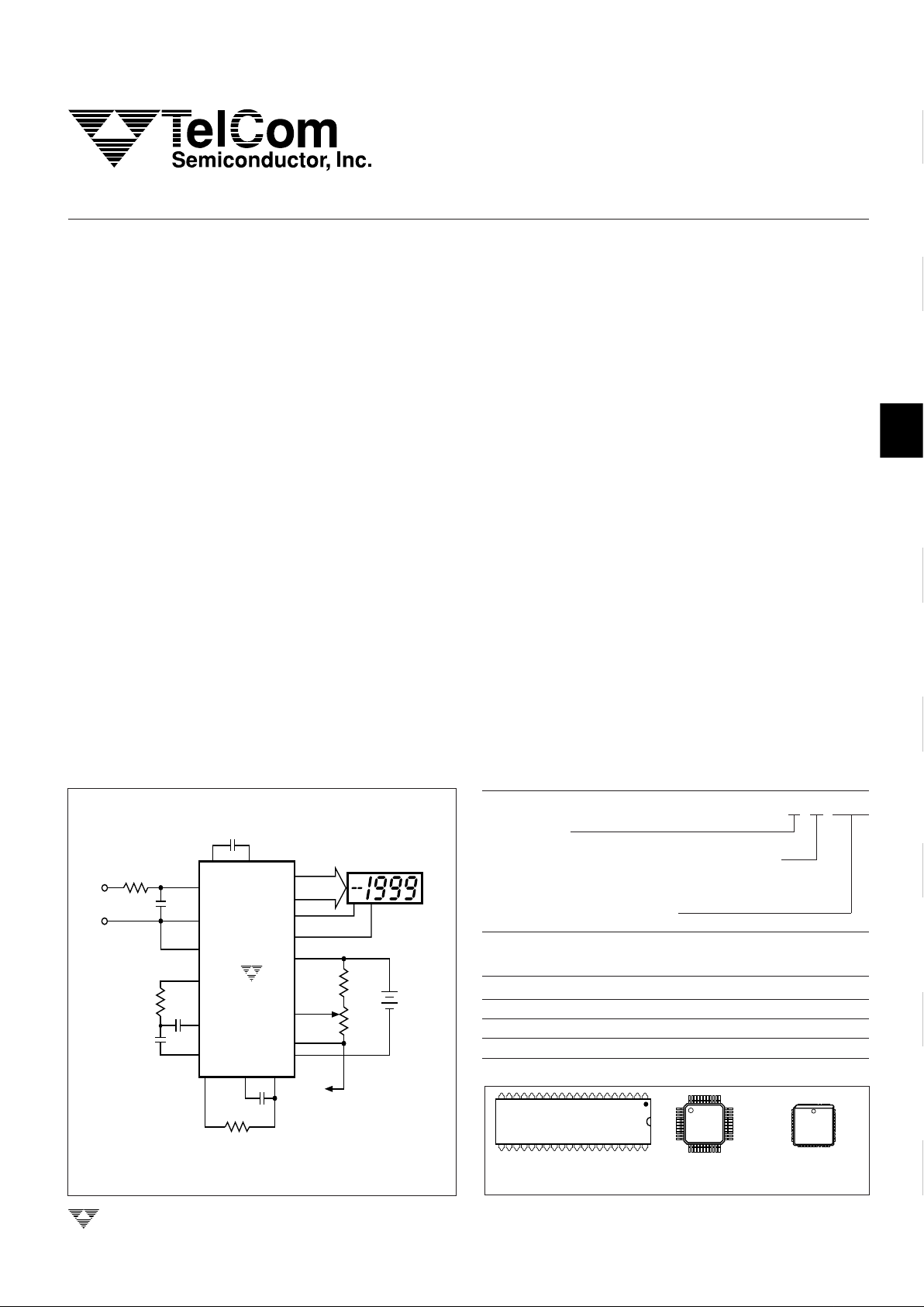
The TC7126A is a 3-1/2 digit CMOS analog-to-digital
converter (ADC) containing all the active components necessary to construct a 0.05% resolution measurement system. Seven-segment decoders, digit and polarity drivers,
voltage reference, and clock circuit are integrated on-chip.
The TC7126A directly drives a liquid crystal display (LCD),
and includes a backplane driver.
A low-cost, high-resolution indicating meter requires
only a display, four resistors, and four capacitors. The
TC7126A's extremely low power drain and 9V battery
operation make it ideal for portable applications.
The TC7126A reduces linearity error to less than 1
count. Roll-over error (the difference in readings for equal
magnitude but opposite polarity input signals) is below ±1
count. High-impedance differential inputs offer 1 pA leakage current and a 1012Ω input impedance. The 15 µV
P-P
noise performance guarantees a "rock solid" reading, and
the auto-zero cycle guarantees a zero display reading with
a 0V input.
The TC7126A features a precision, low-drift internal
voltage reference and is functionally identical to the TC7126.
A low-drift external reference is not normally required with
the TC7126A.
ORDERING INFORMATION
PART CODE TC7126X X XXX
A or blank*
R (reversed pins) or blank (CPL pkg only)
* "A" parts have an improved reference TC
Package Code (see below):
Package Temperature
Code Package Range
CKW 44-Pin PQFP 0°C to +70°C
CLW 44-Pin PLCC 0°C to +70°C
CPL 40-Pin PDIP 0°C to +70°C
IPL 40-Pin PDIP (non-A only) – 25°C to +85°C
V
REF
+
TC7126
TC7126A
33
34
240 kΩ
10 kΩ
31
29
39 38 40
V
REF
–
0.33
µF
0.1 µF
V
–
1
OSC
3
OSC
2
OSC
TO ANALOG COMMON
(PIN 32)
1 CONVERSION/SEC
C
OSC
560 kΩ
180 kΩ
0.15 µF
0.01 µF
ANALOG
INPUT
+
–
C
REF
–
C
REF
+
V
IN
+
V
IN
–
ANALOG
COMMON
V
INT
V
BUFF
C
AZ
20
21
1
SEGMENT
DRIVE
2–19
22–25
POL
BP
V
+
MINUS SIGN
BACKPLANE
28
50 pF
LCD
1 MΩ
27
30
32
35
36
9V
+
R
OSC
26
NOTE: Pin numbers refer to 40-pin DIP.
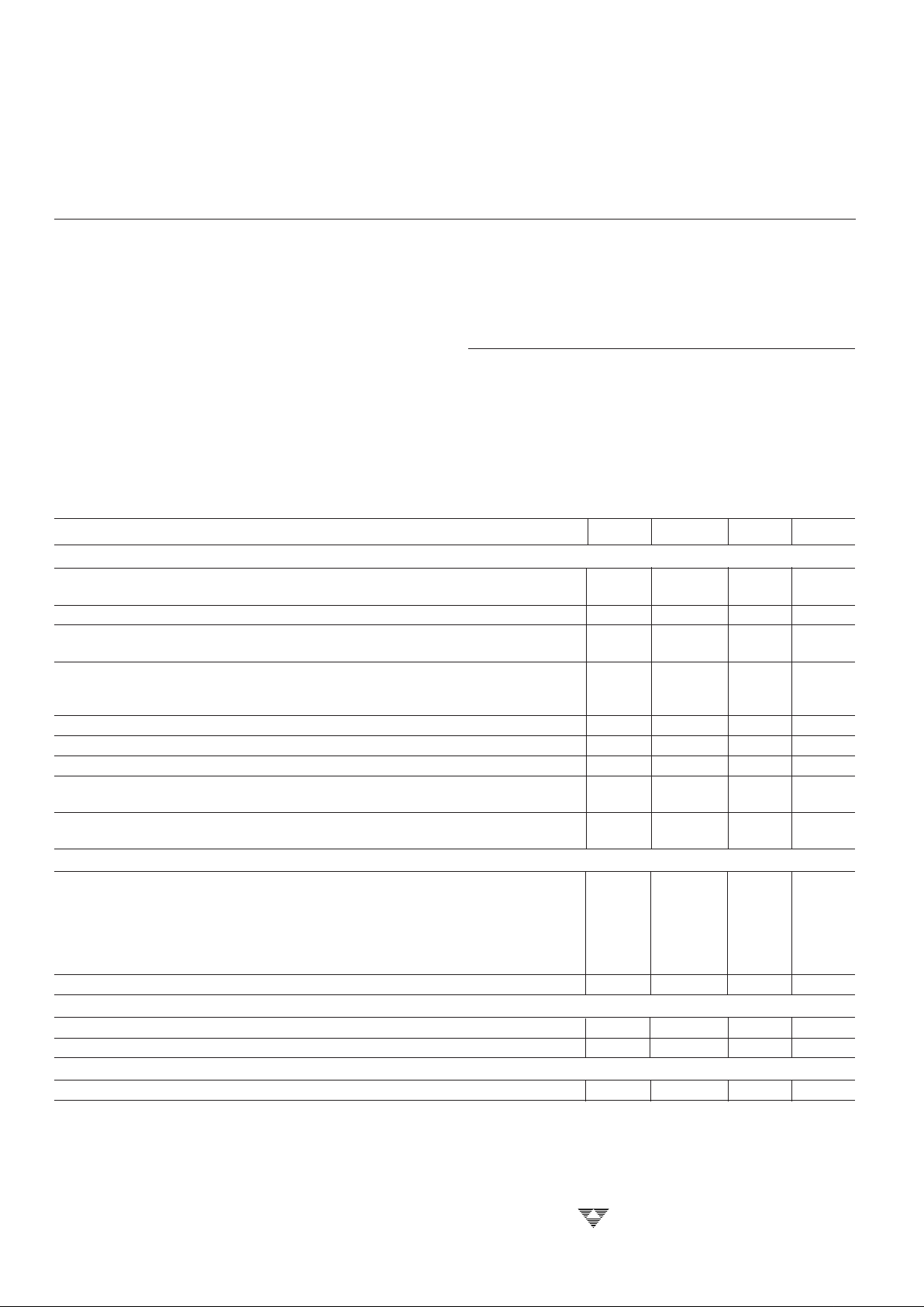
40-Pin Plastic DIP
44-Pin Plastic Quad Flat
Package Formed Leads
44-Pin Plastic Chip
Carrier PLCC
AVAILABLE PACKAGES
TYPICAL OPERATING CIRCUIT
TC7126/A-8 11/6/96
3-218
TELCOM SEMICONDUCTOR, INC.
3-1/2 DIGIT
ANALOG-TO-DIGITAL CONVERTERS
TC7126
TC7126A
ABSOLUTE MAXIMUM RATINGS*
Supply Voltage (V+ to V–)......................................... +15V
Analog Input Voltage (Either Input) (Note 1) ........ V+ to V
–
Reference Input Voltage (Either Input).................V+ to V
–
Clock Input ......................................................TEST to V
+
Operating Temperature Range
C Devices ..............................................0°C to +70°C
I Devices...........................................– 25°C to +85°C
Storage Temperature Range ................– 65°C to +150°C
Lead Temperature (Soldering, 10 sec) .................+300°C
Power Dissipation, (TA ≤ 70°C), (Note 2)
44-Pin PQFP ....................................................1.00W
44-Pin PLCC.....................................................1.23W
40-Pin Plastic PDIP ..........................................1.23W
*Static-sensitive device. Unused devices must be stored in conductive
material. Protect devices from static discharge and static fields. Stresses
above those listed under Absolute Maximum Ratings may cause permanent damage to the device. These are stress ratings only and functional
operation of the device at these or any other conditions above those
indicated in the operational sections of the specifications is not implied.
Exposure to Absolute Maximum Rating Conditions for extended periods
may affect device reliability.
ELECTRICAL CHARACTERISTICS: V
S
= +9V, f
CLK
= 16 kHz, and TA = +25°C, unless otherwise noted.
Symbol Parameter Test Conditions Min Typ Max Unit
Input
Zero Input Reading V
IN
= 0V –000.0 ±000.0 +000.0 Digital
Full Scale = 200 mV Reading
Zero Reading Drift VIN = 0V, 0°C ≤ TA ≤ +70°C — 0.2 1 µV/°C
Ratiometric Reading VIN = V
REF
, V
REF
= 100 mV 999 999/1000 1000 Digital
Reading
NL Linearity Error Full Scale = 200 mV or 2V – 1 ±0.2 1 Count
Max Deviation From Best Fit
Straight Line
Roll-Over Error –VIN = +VIN ≈ 200 mV – 1 ±0.2 1 Count
e
N
Noise VIN = 0V, Full Scale = 200 mV — 15 — µV
P-P
I
L
Input Leakage Current VIN = 0V — 1 10 pA
CMRR Common-Mode Rejection VCM = ±1V, VIN = 0V, — 50 — µV/V
Ratio Full Scale = 200 mV
Scale Factor Temperature VIN = 199 mV, 0°C ≤ TA ≤ +70°C — 1 5 ppm/°C
Coefficient Ext Ref Temp Coeff = 0 ppm/°C
Analog Common
V
CTC
Analog Common 250 kΩ Between Common and V
+
— — — —
Temperature Coefficient 0°C ≤ T
A
≤ +70°C ("C" Devices): — — — —
TC7126 — 80 — ppm/°C
TC7126A — 35 75 ppm/°C
– 25°C ≤ T
A
≤ +85°C ("I" Device):
TC7126A — 35 100 ppm/°C
V
C
Analog Common Voltage 250 kΩ Between Common and V
+
2.7 3.05 3.35 V
LCD Drive
V
SD
LCD Segment Drive Voltage V+ to V– = 9V 4 5 6 V
P-P
V
BD
LCD Backplane Drive Voltage V+ to V– = 9V 4 5 6 V
P-P
Power Supply
I
S
Power Supply Current VIN = 0V, V+ to V– = 9V (Note 6) — 55 100 µA
NOTES: 1. Input voltage may exceed supply voltages when input current is limited to 100 µA.
2. Dissipation rating assumes device is mounted with all leads soldered to PC board.
3. Refer to "Differential Input" discussion.
4. Backplane drive is in-phase with segment drive for "OFF" segment and 180° out-of-phase for "ON" segment. Frequency is 20 times
conversion rate. Average DC component is less than 50 mV.
5. See "Typical Operating Circuit."
6. During auto-zero phase, current is 10–20 µA higher. A 48 kHz oscillator increases current by 8 µA (typical). Common current not
included.

3-219
TELCOM SEMICONDUCTOR, INC.
7
6
5
4
3
1
2
8
3-1/2 DIGIT
ANALOG-TO-DIGITAL CONVERTERS
TC7126
TC7126A
PIN CONFIGURATIONS
27
28
29
30
31
32
33
7
4
3
2
1
NC
TC7126CKW
TC7126ACKW
(FLAT PACKAGE)
12 13 14 15 17 18
G
44 43 42 41 39 3840
COMMON
16
37
C
AZ
36
V
BUFF
35
V
INT
34
V
19 20 21 22
D
26
8
+
25
9
24
10
23
11
5
6
C
OSC
TEST
NC
NC
V
3
3
D2C2B2A
2F2E2
NC
OSC
2
OSC
1
REFCREF
C
–
2
3
A
3
G
3
BP
POL
AB
4
E
3
F
3
B
3
33
34
35
36
37
38
39
13
10
9
8
7
COMMON
V
REF
18 19 20 21 23 24
3
AB
4
POL
NC
BP
NC
B
6543 1442
A
OSC
22
43
OSC42OSC41TEST
40
25 26 27 28
F
E
G
A
C
G
3214
C
AZ
2
3115
V
BUFF
2
3016
V
INT
E
2917
D
NC
11
12
NC
C
D
3
2
F
A
2
2
2
B
3
3
3
3
3
2
TC7126CLW
TC7126ACLW
(PLCC)
1
2
3
V
–
1B1C1D1V+
F
1
G
1
E
1
D
1
C
1
B
1
A
1F1G1E1
+
–
REF
C
REF
C
+
–
–
+
V
IN
V
IN
–
V
REF
+
V
REF
+
V
REF
–
+
VINV
IN
–
TC7126CPL
TC7126ACPL
TC7126IPL
TC7126AIPL
1
2
3
4
OSC
1
5
6
7
8
9
10
11
12
TEST
V
ANALOG
COMMON
C
AZ
V
+
D
NORMAL PIN
CONFIGURATION
13
14
15
16
17
18
19
20
40
39
38
37
36
35
34
33
32
31
30
29
28
27
26
25
24
23
22
21
2
C
2
B
2
A
2
F
2
E
2
D
3
B
3
F
3
E
3
AB
4
10's
100's
1000's
100's
OSC
2
OSC
3
+
REF
V
–
REF
C
+
REF
C
–
REF
V
+
IN
V
–
IN
V
BUFF
V
INT
V
–
G
C
A
G
BP
(BACKPLANE)
POL
(MINUS SIGN)
3
3
3
2
TC7126RCPL
TC7126ARCPL
TC7126RIPL
TC7126ARIPL
1
2
3
4
5
6
7
8
9
10
11
12
13
14
15
16
17
18
19
20
100's
1000's
100's
REVERSE PIN
CONFIGURATION
40
39
38
37
36
35
34
33
32
31
30
29
28
27
26
25
24
23
22
21
D
1
C
1
B
1
A
1
F
1
G
1
E
1
1's
V
+
D
2
C
2
B
2
A
2
F
2
E
2
D
3
B
3
F
3
E
3
AB
4
POL
(MINUS SIGN)
D
1
C
1
B
1
A
1
F
1
G
1
E
1
1's
10's
OSC
TEST
V
ANALOG
COMMON
C
AZ
OSC
2
OSC
+
REF
V
–
REF
C
+
REF
C
–
REF
V
+
IN
V
–
IN
V
BUFF
V
INT
V
–
G
C
A
G
BP
(BACKPLANE)
3
3
3
2
3
1
NC = NO INTERNAL CONNECTION

3-220
TELCOM SEMICONDUCTOR, INC.
3-1/2 DIGIT
ANALOG-TO-DIGITAL CONVERTERS
TC7126
TC7126A
PIN DESCRIPTION
40-Pin PDIP
Pin Number
Normal (Reverse) Name Description
1 (40) V
+
Positive supply voltage.
2 (39) D
1
Activates the D section of the units display.
3 (38) C
1
Activates the C section of the units display.
4 (37) B
1
Activates the B section of the units display.
5 (36) A
1
Activates the A section of the units display.
6 (35) F
1
Activates the F section of the units display.
7 (34) G
1
Activates the G section of the units display.
8 (33) E
1
Activates the E section of the units display.
9 (32) D
2
Activates the D section of the tens display.
10 (31) C
2
Activates the C section of the tens display.
11 (30) B
2
Activates the B section of the tens display.
12 (29) A
2
Activates the A section of the tens display.
13 (28) F
2
Activates the F section of the tens display.
14 (27) E
2
Activates the E section of the tens display.
15 (26) D
3
Activates the D section of the hundreds display.
16 (25) B
3
Activates the B section of the hundreds display.
17 (24) F
3
Activates the F section of the hundreds display.
18 (23) E
3
Activates the E section of the hundreds display.
19 (22) AB
4
Activates both halves of the 1 in the thousands display.
20 (21) POL Activates the negative polarity display.
21 (20) BP Backplane drive output.
22 (19) G
3
Activates the G section of the hundreds display.
23 (18) A
3
Activates the A section of the hundreds display.
24 (17) C
3
Activates the C section of the hundreds display.
25 (16) G
2
Activates the G section of the tens display.
26 (15) V
–
Negative power supply voltage.
27 (14) V
INT
The integrating capacitor should be selected to give the maximum voltage swing
that ensures component tolerance build-up will not allow the integrator output to
saturate. When analog common is used as a reference and the conversion rate is
3 readings per second, a 0.047 µF capacitor may be used. The capacitor must
have a low dielectric constant to prevent roll-over errors. See "Integrating Capaci-
tor" section for additional details.
28 (13) V
BUFF
Integration resistor connection. Use a 180 kΩ resistor for a 200 mV full-scale
range and a 1.8 MΩ resistor for a 2V full-scale range.
29 (12) C
AZ
The size of the auto-zero capacitor influences system noise. Use a 0.33 µF
capacitor for 200 mV full scale, and a 0.033 µF capacitor for 2V full scale. See
paragraph on auto-zero capacitor for more details.
30 (11) V
IN
–
The low input signal is connected to this pin.
31 (10) V
IN
+
The high input signal is connected to this pin.
32 (9) ANALOG This pin is primarily used to set the analog common-mode voltage for battery
operation or in systems where the input signal is referenced to the power supply.
See paragraph on analog common for more details. It also acts as a reference
voltage source.
33 (8) C
REF
–
See pin 34.
COMMON
 Loading...