

TelCom Semiconductor Inc TC7116CPL, TC7116ARIJL, TC7116ARCPL, TC7116ARCKW, TC7116ARCLW Datasheet
...
3-203
TELCOM SEMICONDUCTOR, INC.
7
6
5
4
3
1
2
8
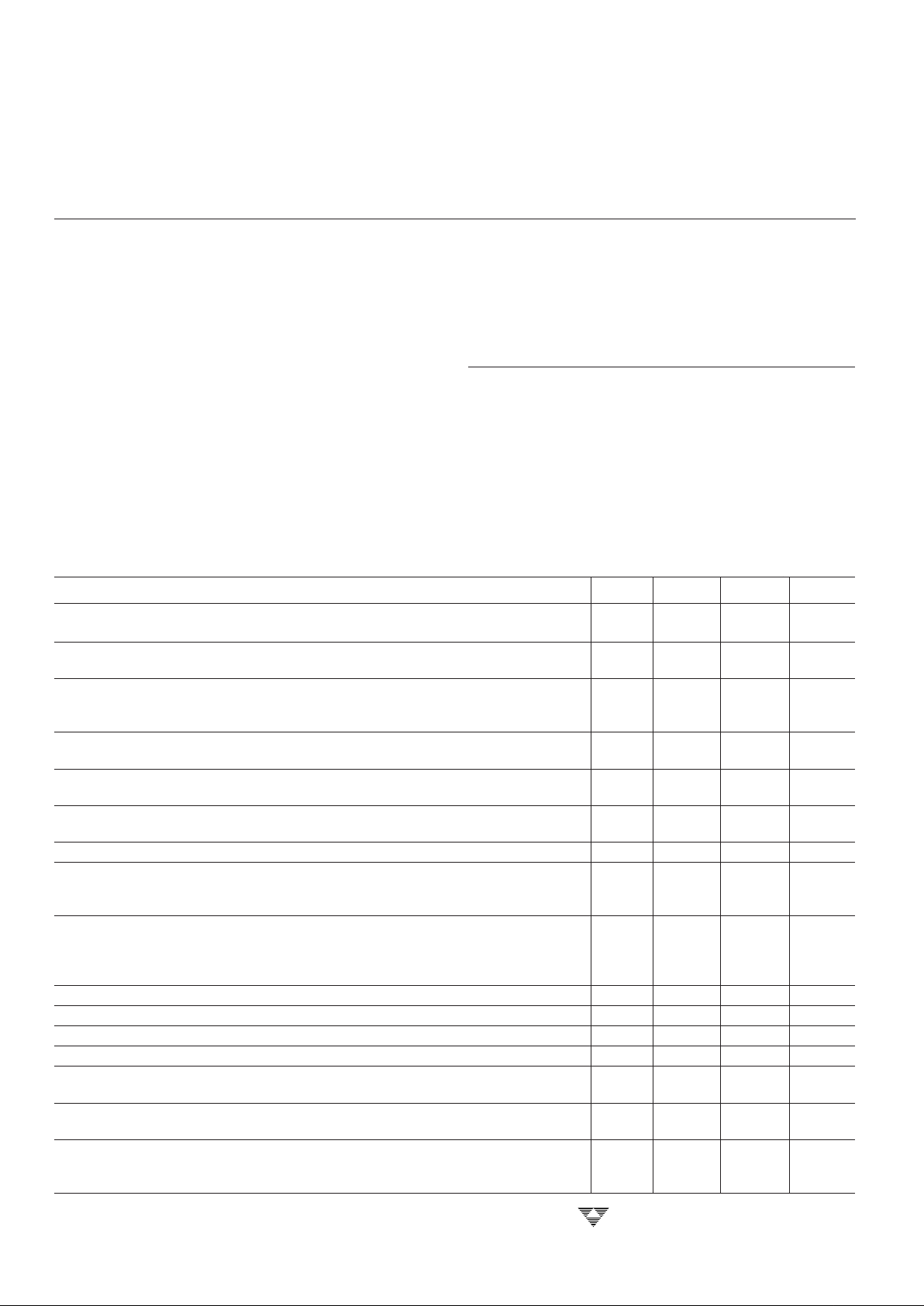
3-1/2 DIGIT ANALOG-T O-DIGITAL CONVERTERS WITH HOLD
V
REF
+
TC7116/A
9V
V
REF
33
34
24 kΩ
1 kΩ
31
29
36
39 38 40
0.47 µF
0.1 µF
V
–
1
OSC
3
OSC
2
OSC
TO ANALOG
COMMON (PIN 32)
3 CONVERSIONS/SEC
C
OSC
100 kΩ
47 kΩ
0.22 µF
0.01 µF
ANALOG
INPUT
+
–
C
REF
–
C
REF
+
V
IN
+
V
IN
–
ANALOG
COMMON
V
INT
V
BUFF
C
AZ
20
21
35
SEGMENT
DRIVE
2–19
22–25
POL
BP/GND
V
+
MINUS SIGN
BACKPLANE
DRIVE
28
R
OSC
100 pF
LCD DISPLAY (TC7116/7116A)
OR COMMON ANODE LED
DISPLAY (TC7117/7117A)
1 MΩ
27
30
32
HLDR
DISPLAY
HOLD
100 mV
1
26
TC7117/A
+
FEATURES
■ Low Temperature Drift Internal Reference
TC7116/TC7117............................. 80 ppm/°C Typ
TC7116A/TC7117A........................20 ppm/°C Typ
■ Display Hold Function
■ Directly Drives LCD or LED Display
■ Guaranteed Zero Reading With Zero Input
■ Low Noise for Stable
Display .........2V or 200 mV Full-Scale Range (FSR)
■ Auto-Zero Cycle Eliminates Need for Zero
Adjustment Potentiometer
■ True Polarity Indication for Precision Null
Applications
■ Convenient 9V Battery Operation
(TC7116/TC7116A)
■ High Impedance CMOS Differential Inputs.... 1012Ω
■ Low Power Operation.................................... 10 mW
GENERAL DESCRIPTION
The TC7116A/TC7117A are 3-1/2 digit CMOS analogto-digital converters (ADCs) containing all the active
components necessary to construct a 0.05% resolution
measurement system. Seven-segment decoders, polarity
and digit drivers, voltage reference, and clock circuit are
integrated on-chip. The TC7116A drives liquid crystal
displays (LCDs) and includes a backplane driver. The
TC7117A drives common anode light emitting diode (LED)
displays directly with an 8-mA drive current per segment.
These devices incorporate a display hold (HLDR)
function. The displayed reading remains indefinitely, as
long as HLDR is held high. Conversions continue, but
output data display latches are not updated. The reference
low input (V
–
REF
) is not available as it is with the TC7106/
7107. V
–
REF
is tied internally to analog common in the
TC7116A/7117A devices.
The TC7116A/7117A reduces linearity error to less
than 1 count. Roll-over error (the difference in readings for
equal magnitude but opposite polarity input signals) is
below ±1 count. High-impedance differential inputs offer 1
pA leakage current and a 1012Ω input impedance. The 15
µV
P-P
noise performance guarantees a “rock solid” reading.
The auto-zero cycle guarantees a zero display reading with
a 0V input.
The TC7116A and TC7117A feature a precision, lowdrift internal reference, and are functionally identical to the
TC7116/TC7117. A low-drift external reference is not
normally required with the TC7116A/TC7117A.
AVAILABLE PACKAGES
40-Pin Plastic
DIP
40-Pin CerDIP
44-Pin Plastic Quad Flat
Package Formed Leads
44-Pin Plastic Chip
Carrier PLCC
Package Temperature
Code Package Range
CKW 44-Pin PQFP 0°C to +70°C
CLW 44-Pin PLCC 0°C to +70°C
CPL 40-Pin Plastic DIP 0°C to +70°C
IJL 40-Pin CerDIP – 25°C to +85°C
Figure 1. Typical TC7116/A/7/A Operating Circuit
TC7116
TC7116A
TC7117
TC7117A
TC7116/A/7117/A-7 10/18/96
ORDERING INFORMATION
PART CODE TC711X X X XXX
6 = LCD
7 = LED
A or blank*
R (reversed pins) or blank (CPL pkg. only)
* "A" parts have an improved reference TC
Package Code (see below):
}
3-204
TELCOM SEMICONDUCTOR, INC.
3-1/2 DIGIT ANALOG-TO-DIGITAL
CONVERTERS WITH HOLD
TC7116
TC7116A
TC7117
TC7117A
ABSOLUTE MAXIMUM RATINGS*
Supply Voltage
TC7116/TC7116A: V+ to V–.................................15V
TC7117/TC7117A: V+ to GND............................. +6V
V– to GND ............................– 9V
Analog Input Voltage (Either Input) (Note 1) ........ V+ to V
–
Reference Input Voltage (Either Input)................. V+ to V
–
Clock Input
TC7116/TC7116A.....................................TEST to V
+
TC7117/TC7117A...................................... GND to V
+
Package Power Dissipation, TA ≤ 70°C (Note 2)
CerDIP..............................................................2.29W
Plastic DIP ........................................................1.23W
Plastic Chip Carrier (PLCC)..............................1.23W
Plastic Quad Flat Package (PQFP) ..................1.00W
Operating Temperature
“C” Device..............................................0°C to +70°C
“I” Device ..........................................– 25°C to +85°C
Storage Temperature ............................– 65°C to +150°C
Lead Temperature (Soldering, 10 sec) ................. +300°C
*Static-sensitive device. Unused devices must be stored in conductive
material. Protect devices from static discharge and static fields. Stresses
above those listed under Absolute Maximum Ratings may cause permanent damage to the device. These are stress ratings only and functional
operation of the device at these or any other conditions above those
indicated in the operational sections of the specifications is not implied.
Exposure to Absolute Maximum Rating Conditions for extended periods
may affect device reliability.
ELECTRICAL CHARACTERISTICS (Note 3)
Parameter Test Conditions Min Typ Max Unit
Zero Input Reading VIN = 0V — ±0 — Digital
Full Scale = 200 mV Reading
Ratiometric Reading VIN = V
REF
999 999/1000 1000 Digital
V
REF
= 100 mV Reading
Roll-Over Error (Difference in –VIN = +VIN ≅ 200 mV or ≈ 2V – 1 ±0.2 +1 Counts
Reading for Equal Positive and
Negative Readings Near Full Scale)
Linearity (Maximum Deviation From Full Scale = 200 mV or 2V – 1 ±0.2 +1 Counts
Best Straight Line Fit)
Common-Mode Rejection Ratio (Note 4) VCM = ±1V, VIN = 0V — 50 — µV/V
Full Scale = 200 mV
Noise (Peak-to-Peak Value Not VIN = 0V — 15 — µV
Exceeded 95% of Time) Full Scale = 200 mV
Leakage Current at Input VIN = 0V — 1 10 pA
Zero Reading Drift V
IN
= 0V
“C” Device: 0°C to +70°C — 0.2 1 µV/°C
“I” Device: –25°C to +85°C—12µv/°C
Scale Factor Temperature Coefficient VIN = 199 mV
“C” Device: 0°C to +70°C — 1 5 ppm/°C
(Ext Ref = 0 ppm/°C)
“I” Device: –25°C to +85°C — — 20 ppm/°C
Input Resistance, Pin 1 Note 6 30 70 — kΩ
VIL, Pin 1 TC7116/A Only — — Test +1.5 V
VIL, Pin 1 TC7117/A Only — — GND +1.5 V
VIH, Pin 1 Both V+ – 1.5 — — V
Supply Current (Does Not Include VIN = 0V — 0.8 1.8 mA
LED Current for 7117/A)
Analog Common Voltage 25 kΩ Between Common 2.4 3.05 3.35 V
(With Respect to Positive Supply) and Positive Supply
Temperature Coefficient of Analog Common "C" Device: 0°C to +70°C
(With Respect to Positive Supply) TC7116A/TC7117A — 20 50 ppm/°C
TC7116/TC7117 — 80 — ppm/°C

3-205
TELCOM SEMICONDUCTOR, INC.
7
6
5
4
3
1
2
8
3-1/2 DIGIT ANALOG-TO-DIGITAL
CONVERTERS WITH HOLD
TC7116
TC7116A
TC7117
TC7117A
ELECTRICAL CHARACTERISTICS (Cont.)
Parameter Test Conditions Min Typ Max Unit
Temperature Coefficient of Analog Common "I" Device: –25°C to +85°C — — 75 ppm/°C
(With Respect to Positive Supply) 25 kΩ Between Common and
Positive Supply (TC7116A/TC7117A)
TC7116/TC7116A ONLY Peak-to-Peak V+ to V– = 9V 4 5 6 V
Segment Drive Voltage (Note 5)
TC7116/TC7116A ONLY Peak-to-Peak V+ to V– = 9V 4 5 6 V
Backplane Drive Voltage (Note 5)
TC7117/TC7117A ONLY Segment V
+
= 5V 5 8 — mA
Sinking Current (Except Pin 19) Segment Voltage = 3V
TC7117/TC7117A ONLY Segment V
+
= 5V 10 16 — mA
Sinking Current (Pin 19 Only) Segment Voltage = 3V
NOTES: 1. Input voltages may exceed supply voltages, provided input current is limited to ±100 µA.
2. Dissipation rating assumes device is mounted with all leads soldered to printed circuit board.
3. Unless otherwise noted, specifications apply at TA = +25°C, f
CLOCK
= 48 kHz. TC7116/TC7116A and TC7117/TC7117A are tested in the
circuit of Figure 1.
4. Refer to "Differential Input" discussion.
5. Backplane drive is in-phase with segment drive for “OFF” segment, 180° out-of-phase for “ON” segment. Frequency is 20 times
conversion rate. Average DC component is less than 50 mV.
6. The TC7116/TC7116A logic inputs have an internal pull-down resistor connected from HLDR, pin 1 to TEST, pin 37.
The TC7117/TC7117A logic inputs have an internal pull-down resistor connected from HLDR, pin 1 to GND, pin 21.

3-206
TELCOM SEMICONDUCTOR, INC.
TC7116
TC7116A
TC7117
TC7117A
BP/
GND
33
34
35
36
37
38
39
13
10
9
8
7
COMMON
V
+
18 19 20 21 23 24
3
AB
4
POL
NC
IN HI
NC
IN LO
B
6543 1442
A
OSC
22
43
OSC42OSC41TEST40REF HI
25 26 27 28
F
E
G
A
C
G
3214
A/Z
2
3115
BUFF
2
3016
INT
E
2917
D
NC
11
12
NC
C
D
3
2
F
A
2
2
2
B
3
3
3
3
3
2
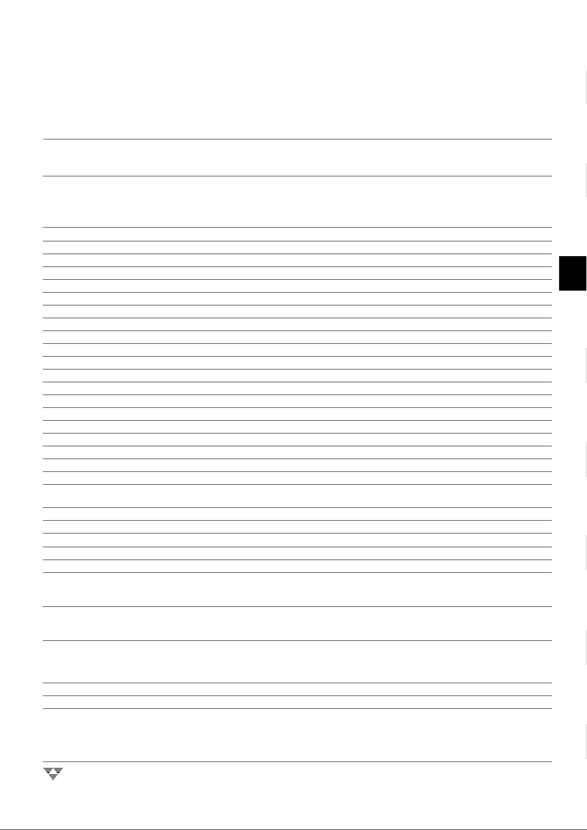
TC7116CLW
TC7116ACLW
TC7117CLW
TC7117ACLW
(PLCC)
1
2
3
V
–
C
REF
C
REF
1B1C1D1
F
1
G
1
E
1
BP/
GND
27
28
29
30
31
32
33
7
4
3
2
1
NC
TC7116CKW
TC7116ACKW
TC7117CKW
TC7117ACKW
12 13 14 15 17 18
G
44 43 42 41 39 3840
REF HI
COMMON
16
37
A/Z36BUFF35INT34V
19 20 21 22
D
26
8
25
9
24
10
23
11
IN HI
5
6
C
OSC
TEST
NC
NC
HLDR
3
3
D2C2B2A
2F2E2
NC
OSC
2
OSC
1
V
+
REFCREF
C
IN LO
–
2
3
A
3
G
3
POL
AB
4
E
3
F
3
B
3
(FLAT PACKAGE)
D
1
C
1
B
1
A
1F1G1E1
TC7116IPL
TC7116AIPL
TC7117CPL
TC7117ACPL
(PDIP)
1
2
3
4
OSC
1
5
6
7
8
9
10
11
12
TEST
V
COMMON
C
AZ
HLDR
D
13
14
15
16
17
18
19
20
40
39
38
37
36
35
34
33
32
31
30
29
28
27
26
25
24
23
22
21
2
C
2
B
2
A
2
F
2
E
2
D
3
B
3
F
3
E
3
AB
4
(MINUS SIGN)
10's
100's
1000's
(TC7116/7117)
(TC7116A/TC7117A)
100's
OSC
2
OSC
3
+
REF
V+
C
+
REF
C
–
REF
V
+
IN
V
–
IN
V
BUFF
V
INT
V
–
G
C
A
G
BP/GND
POL
3
3
3
2
D
1
C
1
B
1
A
1
F
1
G
1
E
1
1's
NOTES:
1. NC = No internal connection.
2. Pins 9, 25, 40, and 56 are connected to the die substrate. The potential at these pins is approximately V . No external connections
should be made.
+
+
–
+
–
HLDR
TC7116IJL
TC7116AIJL
TC7117IJL
TC7117AIJL
(CerDIP)
1
2
3
4
OSC
1
5
6
7
8
9
10
11
12
TEST
V
COMMON
C
AZ
HLDR
D
13
14
15
16
17
18
19
20
40
39
38
37
36
35
34
33
32
31
30
29
28
27
26
25
24
23
22
21
2
C
2
B
2
A
2
F
2
E
2
D
3
B
3
F
3
E
3
AB
4
(MINUS SIGN)
10's
100's
1000's
(TC7116/7117)
(TC7116A/TC7117A)
100's
OSC
2
OSC
3
+
REF
V+
C
+
REF
C
–
REF
V
+
IN
V
–
IN
V
BUFF
V
INT
V
–
G
C
A
G
BP/GND
POL
3
3
3
2
D
1
C
1
B
1
A
1
F
1
G
1
E
1
1's
PIN CONFIGURATIONS
3-1/2 DIGIT ANALOG-TO-DIGITAL
CONVERTERS WITH HOLD
3-207
TELCOM SEMICONDUCTOR, INC.
7
6
5
4
3
1
2
8
PIN DESCRIPTION
40-Pin PDIP/ 44-Pin
40-PinCerDIP Plastic Quad
Pin Number Flat Package
Normal Pin Number Symbol Description
1 8 HLDR Hold pin, Logic 1 holds present display reading.
29D
1
Activates the D section of the units display.
310C
1
Activates the C section of the units display.
411B
1
Activates the B section of the units display.
512A
1
Activates the A section of the units display.
613F
1
Activates the F section of the units display.
714G
1
Activates the G section of the units display.
815E
1
Activates the E section of the units display.
916D
2
Activates the D section of the tens display.
10 17 C
2
Activates the C section of the tens display.
11 18 B
2
Activates the B section of the tens display.
12 19 A
2
Activates the A section of the tens display.
13 20 F
2
Activates the F section of the tens display.
14 21 E
2
Activates the E section of the tens display.
15 22 D
3
Activates the D section of the hundreds display.
16 23 B
3
Activates the B section of the hundreds display.
17 24 F
3
Activates the F section of the hundreds display.
18 25 E
3
Activates the E section of the hundreds display.
19 26 AB
4
Activates both halves of the 1 in the thousands display.
20 27 POL Activates the negative polarity display.
21 28 BP LCD backplane drive output (TC7116/TC7116A).
GND Digital ground (TC7117/TC7117A).
22 29 G
3
Activates the G section of the hundreds display.
23 30 A
3
Activates the A section of the hundreds display.
24 31 C
3
Activates the C section of the hundreds display.
25 32 G
2
Activates the G section of the tens display.
26 34 V
–
Negative power supply voltage.
27 35 V
INT
Integrator output. Connection point for integration
capacitor. See Integration Capacitor section for
additional details.
28 36 V
BUFF
Integration resistor connection. Use a 47 kΩ resistor for
200 mV full-scale range and a 470 kΩ resistor for 2V
full-scale range.
29 37 C
AZ
The size of the auto-zero capacitor influences system
noise. Use a 0.47 µF capacitor for 200 mV full scale and
a 0.047 µF capacitor for 2V full scale. See Auto-Zero
Capacitor paragraph for more details.
30 38 V
–
IN
The analog LOW input is connected to this pin.
31 39 V
+
IN
The analog HIGH input is connected to this pin.
39 40 COMMON This pin is primarily used to set the analog common-
mode COMMON voltage for battery operation or in
systems where the input signal is referenced to the
power supply. See Analog Common paragraph for more
details. It also acts as a reference voltage source.
TC7116
TC7116A
TC7117
TC7117A
3-1/2 DIGIT ANALOG-TO-DIGITAL
CONVERTERS WITH HOLD
 Loading...