

TelCom Semiconductor Inc TC660EPA, TC660EOA, TC660CPA, TC660COA Datasheet
100mA CHARGE PUMP DC-TO-DC VOLT AGE CONVERTER
EVALUATION
KIT
AVAILABLE
FEATURES
■ Pin Compatible with TC7660
■ High Output Current ..................................... 100mA
■ Converts (+1.5V to 5.5V) to (– 1.5V to – 5.5V)
■ Power Efficiency @100mA......................... 88% typ
■ Low Power Consumption ................200µA @ 5 V
■ Low Cost and Easy to Use
— Only Two External Capacitors Required
■ Selectable Oscillator Frequency ....... 10kHz/90kHz
■ ESD Protection ...................................................4kV
APPLICATIONS
■ Laptop Computers
■ µP Based Controllers
■ Process Instrumentation
■ Automotive Instruments
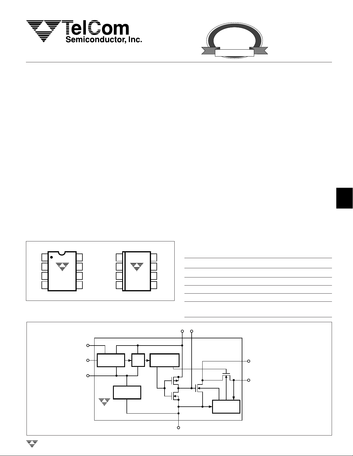
PIN CONFIGURATION (DIP and SOIC)
GENERAL DESCRIPTION
The TC660 DC-to-DC voltage converter generates a
negative voltage supply, that can support a 100mA maximum load, from a positive voltage input of 1.5V to 5.5V. Only
two external capacitors are required.
IN
Power supply voltage is stored on an undedicated
capacitor then inverted and transferred to an output reservoir capacitor. The on-board oscillator normally runs at a
frequency of 10kHz with V+ at 5V. This frequency can be
lowered by the addition of an external capacitor from OSC
(pin 7) to ground, or raised to 90kHz by connecting the
frequency control pin (FC) to V+, in order to optimize capacitor size, quiescent current, and output voltage ripple
frequency. Operation using input voltage between 1.5V and
3.0V is accommodated by grounding the LV input (pin 6).
Operation at higher input voltages (3.0V to 5.5V) is accomplished by leaving LV open.
The TC660 open circuit output voltage is within 0.1% of
the input voltage with the output open-circuited. Power
conversion efficiency is 98% when output load is between
2mA and 5mA.
1
TC660
2
3
4
+
8
V
7
OSC
6
LV
5
V
OUT
FC
CAP
GND
CAP
CAP
GND
CAP
FC
1
+
2
3
–
4
TC660CPA
TC660EPA
FUNCTIONAL BLOCK DIAGRAM
1
FC
OSC
LV
7
6
RC
OSCILLATOR
TC660
1
+
2
TC660COA
3
TC660EOA
–
4
INTERNAL
VOLTAGE
REGULATOR
÷ 2
+
8
V
7
OSC
6
LV
5
V
OUT
VOLTAGE–
LEVEL
TRANSLATOR
ORDERING INFORMATION
Part No. Package Temp. Range
TC660COA 8-Pin SOIC 0°C to +70°C
TC660CPA 8-Pin Plastic DIP 0°C to +70°C
TC660EOA 8-Pin SOIC – 40°C to +85°C
TC660EPA 8-Pin Plastic DIP – 40°C to +85°C
TC7660EV Evaluation Kit for
Charge Pump Family
+
V+CAP
82
4
–
CAP
5
V
OUT
LOGIC
NETWORK
5
6
7
TELCOM SEMICONDUCTOR, INC.
3
GND
8
TC660-2 9/10/96
4-5
TC660
100mA CHARGE PUMP DC-TO-DC
VOLTAGE CONVERTER
ABSOLUTE MAXIMUM RATINGS*
Supply Voltage ........................................................... +6V
LV, FC, OSC Input
Voltage (Note 1) .......................V
Current Into LV (Note 1)...................... 20 µA for V+ >3.5V
Output Short Duration (V
SUPPLY
– 0.3V to (V+ +0.3V)
OUT
≤ 5.5V) (Note 3) ..10 Sec
*Static-sensitive device. Unused devices must be stored in conductive
material. Protect devices from static discharge and static fields. Stresses
above those listed under "Absolute Maximum Ratings" may cause permanent damage to the device. These are stress ratings only and functional
operation of the device at these or any other conditions above those
indicated in the operation sections of the specifications is not implied.
Exposure to absolute maximum rating conditions for extended periods may
affect device reliability.
Power Dissipation (Note 2) (TA ≤ 70°C)
SOIC...............................................................470mW
Plastic DIP ......................................................730mW
Operating Temperature Range
C Suffix ..................................................0°C to +70°C
E Suffix .............................................– 40°C to +85°C
Storage Temperature Range ................– 65°C to +150°C
Lead Temperature (Soldering, 10 sec) .................+300°C
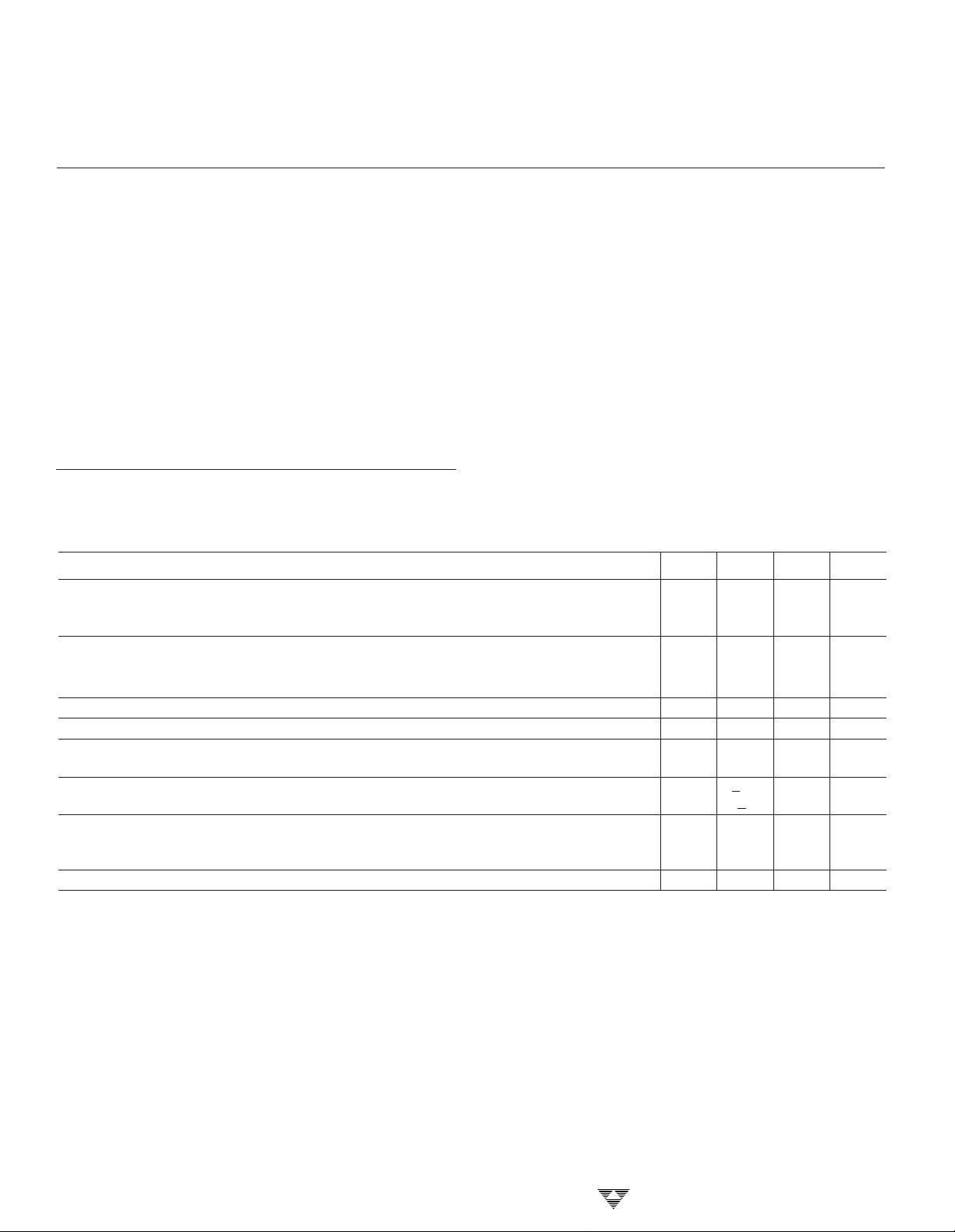
ELECTRICAL CHARACTERISTICS: Specifications Measured Over Operating Temperature Range With,
V+ = 5V, C
(Figure 1), unless otherwise indicated.
Symbol Parameter Test Conditions Min Typ Max Unit
+
I
+
V
R
OUT
I
OUT
F
OSC
I
OSC
P
EFF
V
OUT EFF
NOTES: 1. Connecting any input terminal to voltages greater than V+ or less than GND may cause destructive latch-up. It is recommended that no
Supply Current RL = ∞
FC pin = OPEN or GND — 200 500 µA
FC pin = V
Supply Voltage Range LV = HIGH, RL = 1 kΩ 3 — 5.5 V
LV = GND, RL = 1 kΩ 1.5 — 5.5
LV = OUT, RL = 1 kΩ (Figure 9) 2.5 — 5.5
Output Source Resistance I
Output Current V
= 100mA — 6.5 10 Ω
OUT
< – 4V 100 — — mA
OUT
Oscillator Frequency Pin 7 open; Pin 1 open or GND — 10 — kHz
Pin 1 = V
+
Input Current Pin 1 open —
Pin 1 = V
+
Power Efficiency (Note 4) RL = 1 kΩ connected between V+ & V
= 500Ω connected between V
R
L
IL = 100mA to GND — 88 —
Voltage Conversion Efficiency RL = ∞ 99 99.9 — %
inputs from sources operating from external supplies be applied prior to "power up" of the TC660.
2. Derate linearly above 50°C by 5.5 mW/°C.
3. To prevent damaging the device, do not short V
4. To maximize output voltage and efficiency performance, use low ESR capacitors for C1 and C2.
OUT
to V+.
= Open, C1, C2 = 150µF, FC = Open, Test Circuit
OSC
+
—1 3mA
—90—
+
1.1 — µA
—
OUT
& GND 92 96 —
OUT
96 98 — %
+
5—
4-6
TELCOM SEMICONDUCTOR, INC.

100mA CHARGE PUMP DC-TO-DC
VOLTAGE CONVERTER
TYPICAL CHARACTERISTICS
1
TC660
All curves are generated using the test circuit of Figure 1 with V+ = 5V, LV = GND, FC = open, and TA = +25°C, unless
otherwise noted.
1)
600
500
400
300
200
SUPPLY CURRENT (µA)
100
4)
2.0
1.6
1.2
0.8
0.4
OUTPUT VOLTAGE DROP
FROM SUPPLY VOLTAGE (V)
Supply Current vs.
Supply Voltage
DOUBLER MODE
LV = OUT
LV = OPEN
0
1.5 2.52.0 3.5 5.04.54.03.0 5.5
LV = GND
SUPPLY VOLTAGE (V)
Output Voltage Drop
vs. Load Current
V+ = 3.5V
V+ = 1.5V
V+ = 2.5V
0
04020 1008060
LOAD CURRENT (mA)
V+ = 4.5V
V+ = 5.5V
2) 3)
Supply Current vs.
Oscillator Frequency
10,000
1000
100
SUPPLY CURRENT (µA)
5)
DOUBLER MODE
10
1
0.01 0.1 1 10 100
OSCILLATOR FREQUENCY (kHz)
INVERTING MODE
Output Voltage vs.
Oscillator Frequency
-5.0
I
= 10mA
-4.5
I
= 1mA
LOAD
-4.0
-3.5
OUTPUT VOLTAGE (V)
-3.0
0.1 0.2 0.4 1 4 10 20 402 100
OSCILLATOR FREQUENCY (kHz)
LOAD
I
LOAD
= 80mA
Efficiency vs.
Load Current
100
92
84
76
EFFICIENCY (%)
68
60
04020 1008060
6)
V+ = 3.5V
V+ = 2.5V
V+ = 1.5V
LOAD CURRENT (mA)
Efficiency vs.
Oscillator Frequency
100
96
92
88
84
80
76
72
POWER EFFICIENCY (%)
68
64
60
0.1 0.2 0.4 1 4 10 20 402 100
OSCILLATOR FREQUENCY (kHz)
I
LOAD
I
LOAD
= 1mA
V+ = 5.5V
V+ = 4.5V
= 10mA
I
LOAD
80mA
=
2
3
4
5
6
Output Source Resistance
7)
vs. Supply Voltage
15
12
9
6
3
OUTPUT SOURCE RESISTANCE (Ω)
0
0.5 1.51.0 2.0 3.0 3.5 4.02.5 5.55.04.5
SUPPLY VOLTAGE (V)
TELCOM SEMICONDUCTOR, INC.
Output Source Resistance
8)
vs. Temperature
16
14
12
10
8
6
OUTPUT SOURCE RESISTANCE (Ω)
4
V+ = 1.5VDC
V+ = 3VDC
0
-20-40
20 40
TEMPERATURE (°C)
V+ = 5VDC
8060 100
9)
Oscillator Frequency
vs. Supply Voltage
12
10
8
6
4
2
OSCILLATOR FREQUENCY (kHz)
0
1.0 2.01.5 2.5 3.0 3.5 4.0 4.5 5.0 5.5
LV GROUNDED
FC = OPEN, OSC = OPEN
SUPPLY VOLTAGE (V)
LV OPEN
7
8
4-7
 Loading...