

TelCom Semiconductor Inc TC626100VZB, TC626100VAB, TC626090VAB, TC626090VZB, TC626080VZB Datasheet
...
TEMPERA TURE LIMIT SWITCH
1
TC626*
* PATENTED
FEATURES
■ Requires No External Components
■ On-Chip Temperature Sensing
■ TO-220 package for "Hot Spot" Mounting
■ 50mA Output Signal TO-220 Package (TC626VAB)
■ TO-92 Package for Direct Circuit Board Mounting
APPLICATIONS
■ Vibration-Immune Temperature Sensing
■ Fan Speed Control Circuits
■ System Overtemperature Shutdown
■ Advanced Thermal Warning
■ Consumer Products
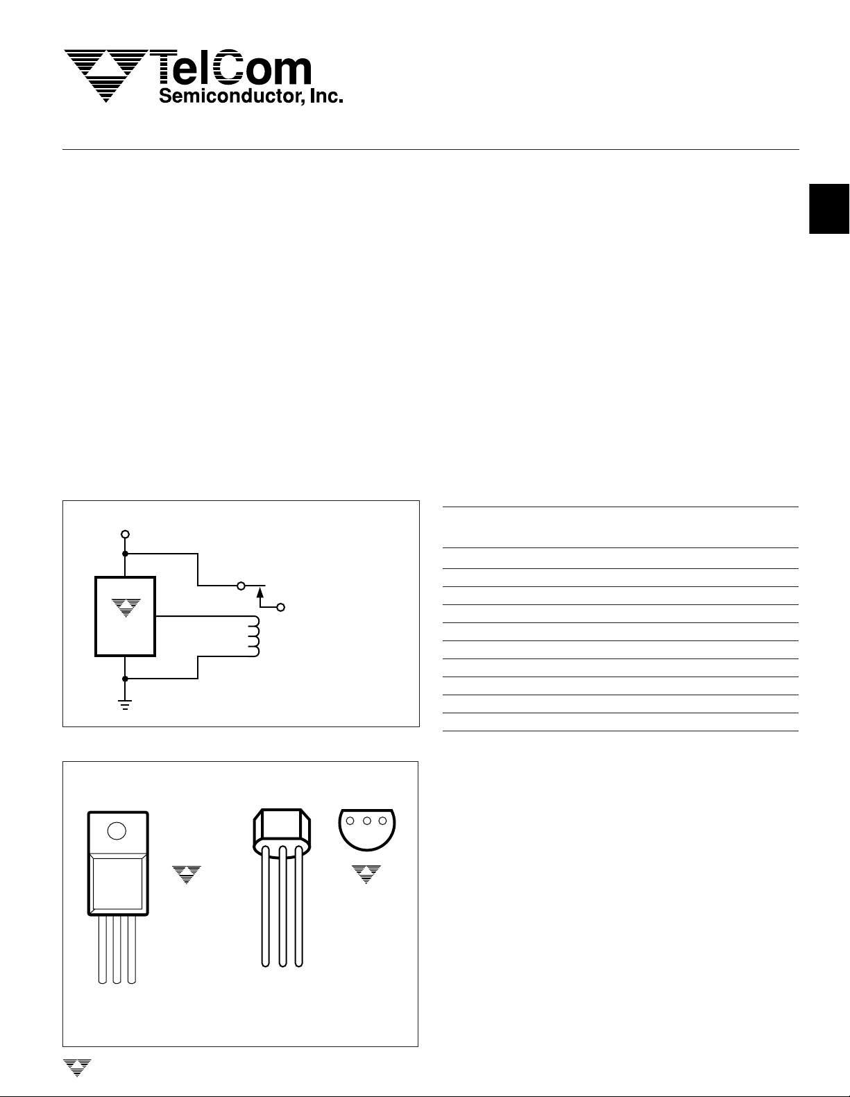
SYSTEM OVERTEMPERATURE PROTECTION
5V TO 18V
2
1
TC626
3
PIN CONFIGURATIONS
TO-220-3 TO-92-3
PIN 1 SWITCHES 'HIGH' IF
TEMPERATURE GOES ABOVE
THE PRESET VALUE.
NC
SYSTEM POWER
RELAY
NC = NORMALLY CLOSED
123
GENERAL DESCRIPTION
The TC626 is a temperature limit detector that notifies
the system when measured temperature is above the factory-programmed setting. It is designed to replace mechanical (bimetal) temperature limit switches and offers increased
ruggedness, higher reliability and greater setpoint accuracy.
It requires no external components.
The TC626 operates over a – 55°C to +125°C temperature range. It is available in a TO-92 package, which is ideal
for ambient temperature sensing applications. It is also
available in a TO-220-3 package for heatsink temperature
measurement applications.
ORDERING INFORMATION
Temperature
Part Number* Package Range
TC626040VAB TO-220-3 – 55°C to +125°C
TC626040VZB TO-92-3 – 55°C to +125°C
TC626050VAB TO-220-3 – 55°C to +125°C
TC626050VZB TO-92-3 – 55°C to +125°C
TC626080VAB TO-220-3 – 55°C to +125°C
TC626080VZB TO-92-3 – 55°C to +125°C
TC626090VAB TO-220-3 – 55°C to +125°C
TC626090VZB TO-92-3 – 55°C to +125°C
TC626100VAB TO-220-3 – 55°C to +125°C
TC626100VZB TO-92-3 – 55°C to +125°C
*Trip-point temperature is designated as follows: Part numbers are
TC626xxxVAB or TC626VZB, where xxx = trip-point tempeature in °C.
For high volume applications requiring different trip-points, contact
factory.
2
3
4
5
6
TC626xxxVAB
123
123
DD
DD
V
OUTPUT
GROUND
TELCOM SEMICONDUCTOR, INC.
V
OUTPUT
GROUND
TC626xxxVZB
7
8
TC626-6 8/23/96
2-29
PRELIMINARY INFORMATION
TC626
TEMPERATURE LIMIT SWITCH
ABSOLUTE MAXIMUM RATINGS*
Package Power Dissipation (TA ≤ 70°C)
TO-92 ...........................................................440mW
TO-220 ............................................................1.6mW
*Stresses above those listed under "Absolute Maximum Ratings" may
cause permanent damage to the device. These are stress ratings only and
functional operation of the device at these or any other conditions above
those indicated in the operation sections of the specifications is not implied.
Exposure to absolute maximum rating conditions for extended periods may
affect device reliability.
Supply Voltage ............................................................20V
Input Voltage Any Input......(GND – 0.3V) to (VDD + 0.3V)
Operating Temperature.........................– 55°C to +125°C
Maximum Junction Temperature...........................+150°C
Storage Temperature ............................– 65°C to +150°C
Lead Temperature (Soldering, 10 sec) .................+300°C
ELECTRICAL CHARACTERISTICS: V
= +5V and TA = – 55°C to +125°C, unless otherwise specified.
DD
Parameter Test Conditions Min Typ Max Units
Supply Voltage 4.5 — 18 V
Supply Current — 300 600 µA
Output Resistance Output High or Low — — 75 Ω
Output Current Source/Sink, VCC = 18V — — 25 mA
Source/Sink, VCC = 4.5V — — 10 mA
Absolute Accuracy At trip point T – 3 T T + 3 °C
Trip Point Hysteresis 3.5 5 6.5 °C
TelCom Semiconductor reserves the right to make changes in the circuitry or specifications detailed in this manual at any time without notice. Minimums
and maximums are guaranteed. All other specifications are intended as guidelines only. TelCom Semiconductor assumes no responsibility for the use of
any circuits described herein and makes no representations that they are free from patent infringement.
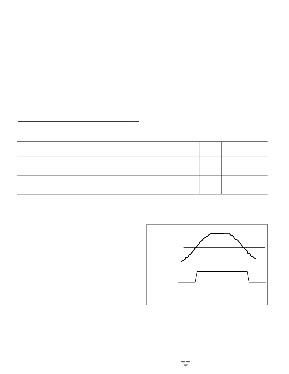
DETAILED DESCRIPTION
The TC626 output maintains a logic low state when
measured temperature is below the factory-programmed
setting. As temperature rises, the output is driven active to
a high level [VDD – (I
the setpoint value ±3°C.
Built-in hysteresis prevents output "chattering" when
measured temperature is at (or near) the trip point (Figure 1).
As temperature falls through the trip point, hysteresis maintains the output high until measured temperature is 5°C
lower than the trip point setting.
The TC626VZB (TO-92 package) has a maximum output current of 10mA while the TC626VAB has a maximum
output current of 50mA. Care must be taken to observe
these output current limits as output currents in excess of
those stated will cause device self-heating resulting in
erroneous temperature measurements.
OUT
)(R
)] when temperature equals
OUT
SET POINT
(SET POINT – 5°C)
OUTPUT
Figure 1. TC626 Operation
2-30
TELCOM SEMICONDUCTOR, INC.
 Loading...