

TelCom Semiconductor Inc TC621HCPA, TC621HEOA, TC621HCOA, TC621CEPA, TC621CCPA Datasheet
...
5V , DUAL TRIP POINT TEMPERA TURE SENSORS
1
TC620
TC621
FEATURES
■ User-Programmable Hysteresis and Temperature
Set Point
■ Easily Programs with 2 External Resistors
■ Wide Temperature Detection
Range................ – 40°C to +125°C (TC620/621CVx)
■ External Thermistor for Remote Sensing
Applications (TC621x)
APPLICATIONS
■ Power Supply Overtemperature Detection
■ Consumer Equipment
■ Temperature Regulators
■ CPU Thermal Protection
ORDERING INFORMATION
Ambient
Part No. Package Temperature
TC620x*COA 8-Pin SOIC 0°C to +70°C
TC620x*CPA 8-Pin Plastic DIP 0°C to +70°C
TC620x*EOA 8-Pin SOIC – 40°C to +85°C
TC620x*EPA 8-Pin Plastic DIP – 40°C to +85°C
TC620CVOA 8-Pin SOIC – 40°C to +125°C
TC621x*COA 8-Pin SOIC 0°C to +70°C
TC621x*CPA 8-Pin Plastic DIP 0°C to +70°C
GENERAL DESCRIPTION
The TC620 and TC621 are programmable logic output
temperature detectors designed for use in thermal management applications. The TC620 features an on-board temperature sensor, while the TC621 connects to an external
NTC thermistor for remote sensing applications.
Both devices feature dual thermal interrupt outputs
(HIGH LIMIT and LOW LIMIT), each of which program with
a single external resistor. On the TC620, these outputs are
driven active (high) when measured temperature equals the
user-programmed limits. The CONTROL (hysteresis) output is driven high when temperature equals the high limit
setting, and returns low when temperature falls below the
low limit setting. This output can be used to provide simple
ON/OFF control to a cooling fan or heater. The TC621
provides the same output functions except that the logical
states are inverted.
The TC620/621 are usable over a maximum temperature range of – 40°C to +125°C.
Ambient
Part No. Package Temperature
TC621x*EOA 8-Pin SOIC – 40°C to +85°C
TC621x*EPA 8-Pin Plastic DIP – 40°C to +85°C
*The part code will be C or H (see Functional Block Diagram, below,
and page 2).
2
3
4
5
FUNCTIONAL BLOCK DIAGRAM
Temp
to
Voltage
Converter
V
LOW SET
HIGH SET
2
3
REF
GEN
V
REF
V
REF
GEN
TELCOM SEMICONDUCTOR, INC.
TC620
+
–
+
–
R
Q
V
DD
8
Thermistor
1
4
7
LOW LIMIT
6
HIGH LIMIT
S
Q
5
CONTROL*
*Suffix code "C" denotes cooling option (high true CONTROL output);
suffix code "H" denotes heating option (low true CONTROL output).
THERMISTOR
HIGH SET
LOW SET
Interface
Circuit
V
2
GEN
V
3
V
GEN
REF
REF
REF
V
DD
8
TC621
+
–
4
7
HIGH LIMIT
6
7
+
–
R
Q
6
LOW LIMIT
S
Q
5
CONTROL*
8
TC620/1-9 11/4/96
2-15
TC620
TC621
5V , DUAL TRIP POINT
TEMPERATURE SENSORS
ABSOLUTE MAXIMUM RATINGS*
Maximum Chip Temperature.................................+150°C
Storage Temperature ............................– 65°C to +150°C
Package Power Dissipation (TA ≤ 70°C)
PDIP ...............................................................730mW
SOIC...............................................................470mW
Derating Factors
Plastic ............................................................8mW/°C
Supply Voltage ............................................................20V
Input Voltage Any Input....... (GND – 0.3V) to (VDD +0.3V)
Operating Temperature
M Version .......................................– 55°C to +125°C
Lead Temperature (Soldering, 10 sec) ................. +300°C
*Static-sensitive device. Unused devices must be stored in conductive
material. Protect devices from static discharge and static fields. Stresses
above those listed under "Absolute Maximum Ratings" may cause permanent damage to the device. These are stress ratings only and functional
operation of the device at these or any other conditions above those
indicated in the operation sections of the specifications is not implied.
Exposure to absolute maximum rating conditions for extended periods may
affect device reliability.
V Version ........................................– 40°C to +125°C
E Version ..........................................– 40°C to +85°C
C Version............................................... 0°C to +70°C
ELECTRICAL CHARACTERISTICS: T
= 25°C, unless otherwise specified.
A
Parameter Conditions Min Typ Max Unit
Supply Voltage Range 4.5 — 18 V
Supply Current 5V ≤ VDD ≤ 18V — 270 400 µA
Output Resistance Output High or Low, 5V ≤ VDD ≤ 18V — 400 1000 Ω
Output Current Temp Sensed Source/Sink — — 1 mA
Output Current Cool/Heat Source/Sink — — 1 mA
Absolute Accuracy T = Programmed Temperature T – 3 T T + 3 °C
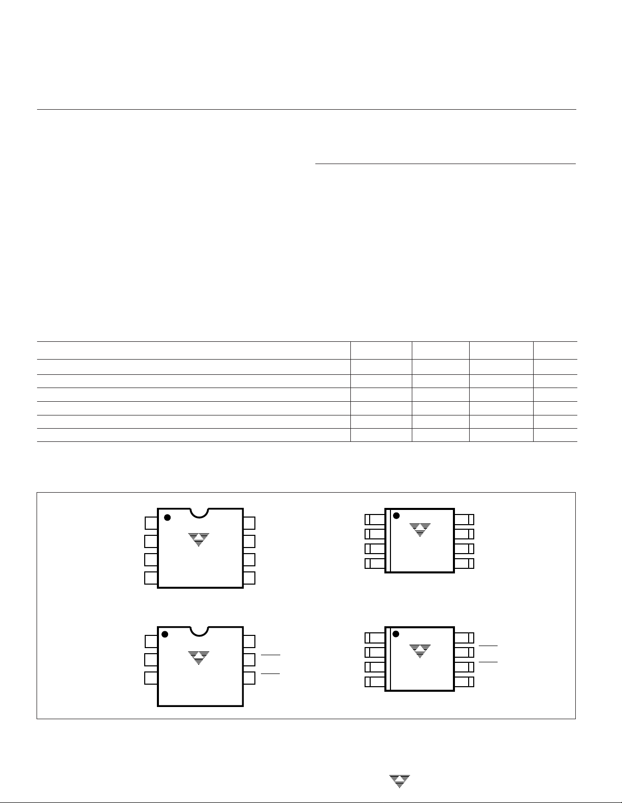
PIN CONFIGURATIONS (DIP and SOIC)
1
NC
GND
NC
GND
2
3
4
1
2
3
4
TC620xCPA
TC620xEPA
TC621xCPA
TC621xEPA
LOW SET
HIGH SET
HIGH SET
LOW SET
V
8
DD
LOW LIMIT
7
HIGH LIMIT
6
5
CONTROL
8
V
DD
HIGH LIMIT
7
6
LOW LIMIT
CONTROL
5
NC
LOW SET
HIGH SET
GND
NC
HIGH SET
LOW SET
GND
1
2
TC620xCOA
3
TC620xEOA
4
TC620CVOA
1
2
TC621xCOA
3
TC621xEOA
4
8
7
6
5
8
7
6
5
V
DD
LOW LIMIT
HIGH LIMIT
CONTROL
V
DD
HIGH LIMIT
LOW LIMIT
CONTROL
2-16
TELCOM SEMICONDUCTOR, INC.
 Loading...