

TelCom Semiconductor Inc TC55RP6002EMB, TC55RP5902EZB, TC55RP6001ECB, TC55RP5902EMB, TC55RP5902ECB Datasheet
...
4-127
TELCOM SEMICONDUCTOR, INC.
7
6
5
4
3
1
2
8
TC55 Series
FEATURES
■ Very Low Dropout Voltage.... 120mV typ at 100mA
380mV typ at 200mA
■ High Output Current .............. 250mA (V
OUT
= 5.0V)
■ High Accuracy Output Voltage........................± 2%
(± 1% Semicustom Version)
■ Wide Output Voltage Range .................... 2.1V-6.0V
■ Low Power Consumption ................... 1.1µA (Typ.)
■
Low Temperature Drift ...................± 100ppm/°C Typ
■ Excellent Line Regulation ..................... 0.2%/V Typ
■ Package Options ....................................SOT-23A-3
SOT-89-3
TO-92
■ Short Circuit Protected
■ Standard 3.0V, 3.3V and 5.0V Output Voltages
■ Custom Voltages Available from 2.1V to 6.0V in
0.1V Steps.
APPLICATIONS
■ Battery-Powered Devices
■ Cameras and Portable Video Equipment
■ Pagers and Cellular Phones
■ Solar-Powered Instruments
■ Consumer Products
GENERAL DESCRIPTION
The TC55 Series is a collection of CMOS low dropout
positive voltage regulators which can source up to 250mA of
current with an extremely low input-output voltage differential of 380mV.
The low dropout voltage combined with the low current
consumption of only 1.1µA makes this part ideal for battery
operation. The low voltage differential (dropout voltage)
extends battery operating lifetime. It also permits high currents in small packages when operated with minimum VIN –
V
OUT
differentials.
The circuit also incorporates short-circuit protection to
ensure maximum reliability.
LOW DROPOUT POSITIVE VOL T AGE REGULA TOR
Output Voltage:
Ex: 21= 2.1V; 60 = 6.0V
Extra Feature Code: Fixed: 0
Tolerance:
1 = ±1.0% (Custom)
2 = ±2.0% (Standard)
Temperature: E: – 40°C to +85°C
Package Type and Pin Count:
CB: SOT-23A-3 (Equivalent to EIAJ (SC-59))
MB: SOT-89-3
ZB: TO-92-3
Taping Direction:
Standard Taping
Reverse Taping
No suffix: TO-92 Bulk
PART CODE TC55 RP XX X X X XX XXX
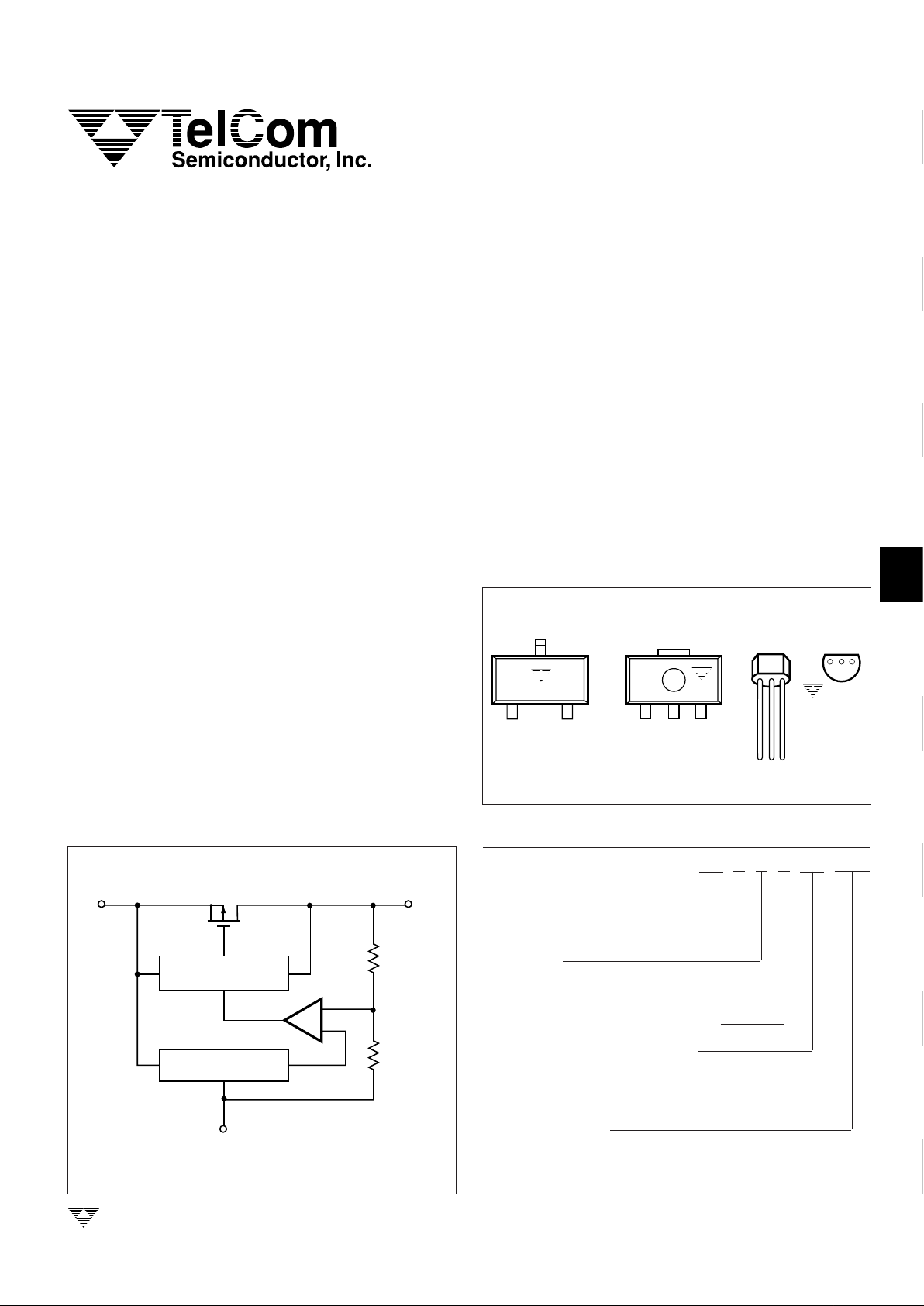
ORDERING INFORMATION
PIN CONFIGURATIONS
FUNCTIONAL BLOCK DIAGRAM
V
IN
V
OUT
GND
+
–
Short-circuit
Protection
Voltage
Reference
TC55-20 11/8/96
132
V
IN
V
IN
V
IN
V
OUT
V
OUT
V
OUT
GND
GND
GND
TC55
TC55
TC55
11233
2
*SOT-23A-3
SOT-89-3 TO-92
*SOT-23A-3 is equivalent to EIAJ (SC-59)
4-128
TELCOM SEMICONDUCTOR, INC.
TC55 Series
LOW DROPOUT
POSITIVE VOLT AGE REGULATOR
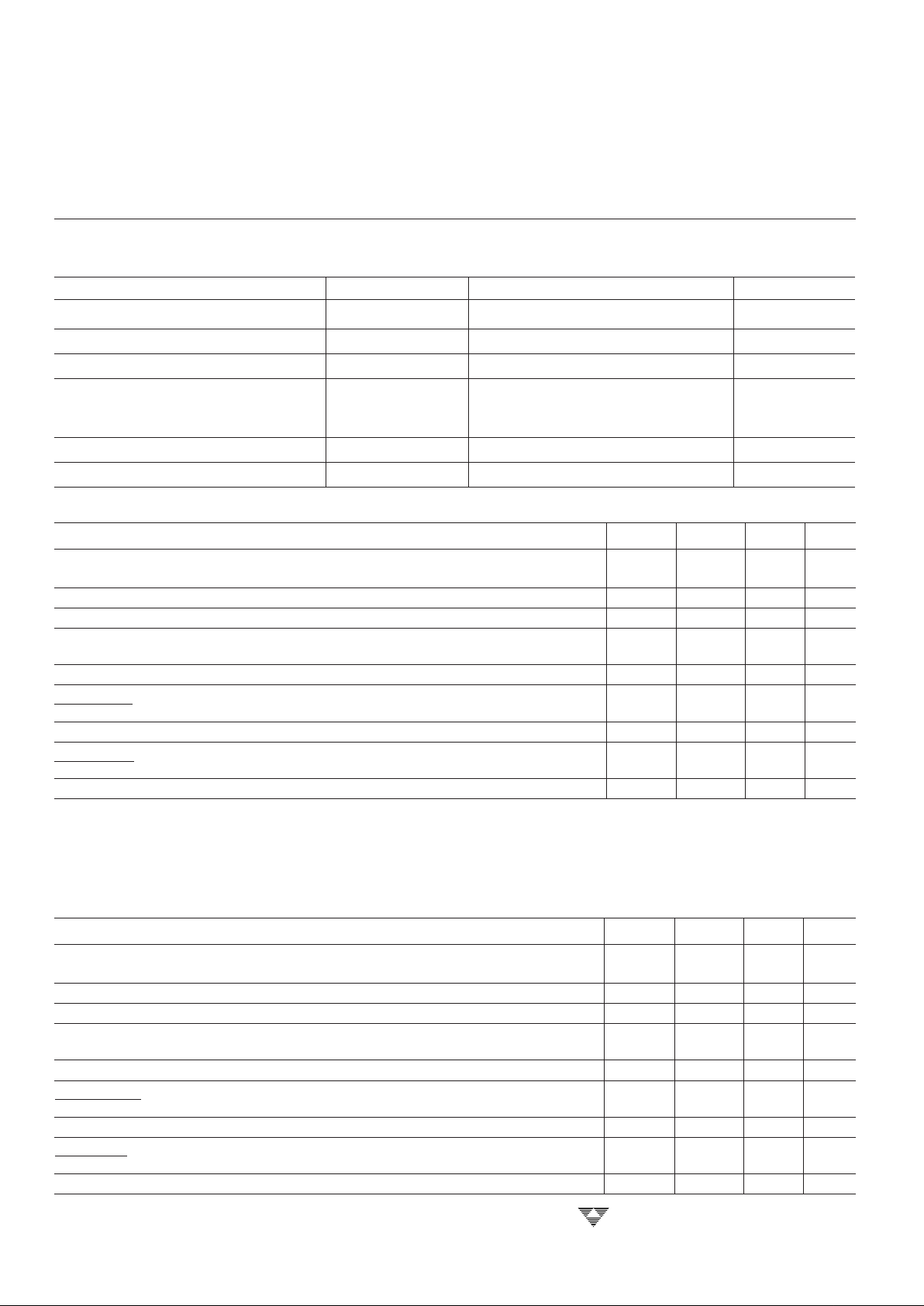
TC55RP50 ELECTRICAL CHARACTERISTICS:
V
OUT
(S) = 5.0V, TA = 25°C unless otherwise specified (see REMARKS).
Symbol Parameter Test Conditions Min Typ Max Unit
V
OUT
(A) Output Voltage I
OUT
= 40mA — — — V
VIN = 6.0V 4.90 5.0 5.10
I
OUT
max Maximum Output Current VIN = 6.0V, V
OUT
(A) ≥ 4.5V 250 — — mA
∆V
OUT
Load Regulation VIN = 6.0 V, 1 mA ≤ I
OUT
≤ 100mA — 40 80 mV
V
dif
I/O Voltage Difference I
OUT
= 100mA — 120 300 mV
I
OUT
= 200 mA — 380 600
I
SS
Current Consumption VIN = 6.0V — 1.1 3.0 µA
V
OUT
(A)·100 Voltage Regulation I
OUT
= 40mA — 0.2 0.3 %/V
∆VIN·V
OUT
(S) 6.0V ≤ VIN ≤ 10.0V
V
IN
Input Voltage — — 10.0 V
∆V
OUT
(A)·10
6
Temperature Coefficient I
OUT
= 40mA — ±100 — ppm/°C
V
OUT
(S)·∆T
A
of Output Voltage – 40°C ≤ TA ≤ 85°C
Long Term Stability TA = 125°C, 1000 Hours — 0.5 — %
REMARKS:V
OUT
(S): Preset value of Output voltage
V
OUT
(A): Actual value of Output voltage
V
dif
: Definition of I/O voltage difference = {VIN1 – V
OUT
(A)}
V
OUT
(A): Output Voltage when I
OUT
is fixed and VIN = V
OUT
(S) + 1.0V
VIN1: Input Voltage when the output voltage is 98% V
OUT
(A)
TC55RP40 ELECTRICAL CHARACTERISTICS:
V
OUT
(S) = 5.0V, TA = 25°C unless otherwise specified (see REMARKS).
Symbol Parameter Test Conditions Min Typ Max Unit
V
OUT
(A) Output Voltage I
OUT
= 40mA — — — V
VIN = 5.0V 3.92 4.0 4.08
I
OUT
max Maximum Output Current VIN = 5.0V, V
OUT
(A) ≥ 3.6V 200 — — mA
∆V
OUT
Load Regulation VIN = 5.0 V, 1 mA ≤ I
OUT
≤ 100mA — 45 90 mV
V
dif
I/O Voltage Difference I
OUT
= 100mA — 170 330 mV
I
OUT
= 200mA — 400 630
I
SS
Current Consumption VIN = 5.0V — 1.0 2.9 µA
∆V
OUT
(A)·100 Voltage Regulation I
OUT
= 40mA — 0.2 0.3 %/V
∆VIN·V
OUT
(S) 5.0V ≤ VIN ≤ 10.0V
V
IN
Input Voltage — — 10.0 V
∆V
OUT
(A) Temperature Coefficient I
OUT
= 40mA — ±100 — ppm/°C
V
OUT
(S)·∆T
A
of Output Voltage – 40°C ≤ TA ≤ 85°C
Long Term Stability TA = 125°C, 1000 Hours — 0.5 — %
ABSOLUTE MAXIMUM RATINGS*
Item Code Ratings Units
Input Voltage V
IN
+12 V
Output Current I
OUT
Pd/(VIN – V
OUT
)mA
Output Voltage V
OUT
(VSS – 0.3) to (VIN + 0.3) V
Power Dissipation: SOT-23A-3 Pd 240 mW
(TA ≤ 70°C) SOT-89 400
TO-92 440
Operating Temperature Range T
A
– 40 to +85 °C
Storage Temperature Range T
stg
– 65 to +150 °C
 Loading...