

TelCom Semiconductor Inc TC54VN6002EMB, TC54VN6002EZB, TC54VN6002ECB, TC54VN6001EZB, TC54VN5802EZB Datasheet
...
VOL TAGE DETECTOR
FEATURES
1
TC54
2
GENERAL DESCRIPTION
■ Precise Detection Thresholds .... Standard ± 2.0%
Custom ± 1.0%
■ Small Packages ...........SOT-23A-3, SOT-89, TO-92
■ Low Current Drain ..................................... Typ. 1µA
■ Wide Detection Range..........................2.1V to 6.0V
■ Wide Operating Voltage Range ............1.5V to 10V
APPLICATIONS
■ Battery Voltage Monitoring
■ Microprocessor Reset
■ System Brownout Protection
■ Switching Circuit in Battery Backup
■ Level Discriminator
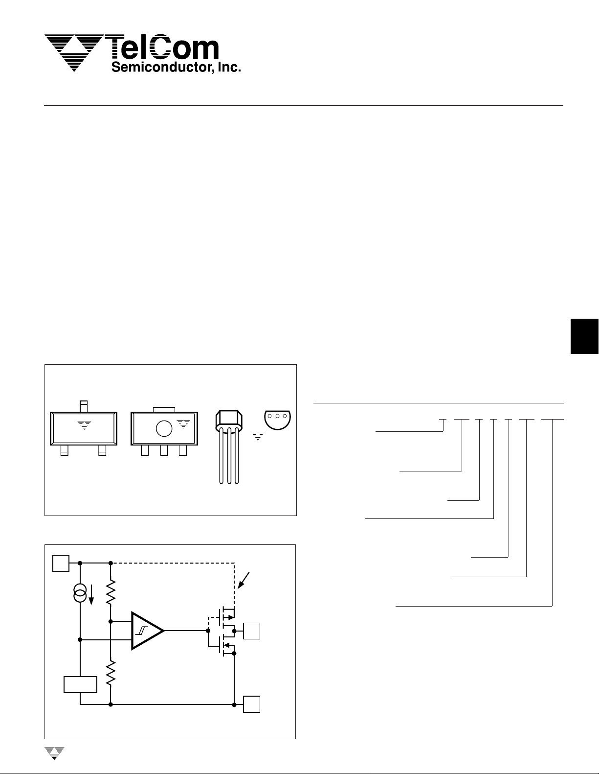
PIN CONFIGURATIONS
*SOT-23A-3 SOT-89-3
V
IN
TC54
V
OUT
*SOT-23A-3 is equivalent to EIAJ (SC-59)
FUNCTIONAL BLOCK DIAGRAM
V
SS
132
V
OUT
TC54
V
V
IN
SS
OUT
V
TO-92
IN
SS
V
V
112332
TC54
The TC54 Series are CMOS voltage detectors, suited
especially for battery-powered applications because of their
extremely low 1µA operating current and small surfacemount packaging. Each part is laser trimmed to the desired
threshold voltage which can be specified from 2.1V to 6.0V,
in 0.1V steps.
The device includes a comparator, low-current highprecision reference, laser-trimmed divider, hysteresis circuit
and output driver. The TC54 is available with either an opendrain or complementary output stage.
In operation, the TC54's output (V
logic HIGH state as long as VIN is greater than the
specified threshold voltage (V
–
V
, the output is driven to a logic LOW. V
DET
LOW until VIN rises above V
whereupon it resets to a logic HIGH.
–
). When VIN falls below
DET
–
by an amount V
DET
) remains in the
OUT
OUT
remains
HYST
ORDERING INFORMATION
PART CODE TC54 V X XX X X X XX XXX
Output form:
N = Nch Open Drain
C = CMOS Output
Detected Voltage:
Ex: 21 = 2.1V; 60 = 6.0V
Extra Feature Code: Fixed: 0
Tolerance:
1 = ± 1.0% (custom)
2 = ± 2.0% (standard)
3
4
,
5
6
2
V
IN
–
+
V
REF
TC54VN has open-drain output.
TC54VC has complementary output.
TELCOM SEMICONDUCTOR, INC.
TC54VC only
V
OUT
1
V
SS
3
Temperature: E: – 40°C to + 85°C
Package Type and Pin Count:
CB: SOT-23A-3*, MB: SOT-89-3, ZB: TO-92-3
Taping Direction:
Standard Taping
Reverse Taping
No suffix: TO-92 Bulk
*SOT-23A-3 is equivalent to EIAJ (SC-59).
7
8
TC54-10 11/8/96
4-279
TC54
VOLT AGE DETECTOR
ABSOLUTE MAXIMUM RATINGS*
Supply Voltage (V
Output Voltage: CMOS ............ (VSS – 0.3) to (VIN + 0.3)
Output Current .........................................................50mA
Power Dissipation: (TA ≤ 70°C)
..................................................................... 12V
IN)
Open Drain................. (VSS – 0.3) to 12V
* Static-sensitive device. Unused devices must be stored in conductive
material. Protect devices from static discharge and static fields. Stresses
above those listed under Absolute Maximum Ratings may cause permanent damage to the device. These are stress ratings only and functional
operation of the device at these or any other conditions above those
indicated in the operational sections of the specifications is not implied.
Exposure to Absolute Maximum Rating Conditions for extended periods
may affect device reliability.
SOT-23A-3 .....................................................240mW
SOT-89-3 .......................................................400mW
TO-92 .......................................................440mW
Operating Temperature..........................– 40°C to + 85°C
Storage Temperature ........................... – 65°C to + 150°C
Soldering Temperature ...................... 300°C, 10 seconds
ELECTRICAL CHARACTERISTICS: T
= 25°C, unless otherwise specified.
A
Symbol Parameter Test Conditions Min Typ Max Unit
V
I
SS
V
V
I
OUT
IN
–
DET
HYST
Operating Voltage V
Quiescent Current VIN = 2.1V 1.0 3.0
Threshold Voltage (V
Hysteresis Range (V
Output Current Nch VDS = 0.5 VIN = 2.1V 7.7 mA
–
= 2.1 to 6.0V 1.5 10.0 V
DET
3.0V 1.3 3.4 µA
4.0V 1.6 3.8
5.0V 2.0 4.2
–
)(V
DET
–
DET
x 0.98 x 1.02
–
)(V
DET
–
)(V
DET
–
DET
x 0.02 x 0.05 x 0.08
3.0V 10.1
4.0V 11.5
5.0V 13.0
)V
)V
Pch VDS = 2.1V VIN = 8.0V – 10.0
TC (V
–
) Tempco of (V
DET
–
) – 40°C ≤ TA ≤ 85°C ± 100 ppm/°C
DET
PIN DESCRIPTION
Pin No. Symbol Description
1VINAnalog input. This pin is both the power supply input and the voltage to be monitored.
2V
OUT
Digital output. This output goes low when VIN drops below V
high when VIN rises above V
–
DET
+ V
. (See timing chart).
HYST
3VSSGround terminal.
4-280
TELCOM SEMICONDUCTOR, INC.
–
and returns
DET

VOLT AGE DETECTOR
1
TC54
TIMING CHART
V
DETECT VOLTAGE V
MINIMUM OPERATING
GROUND LEVEL
OUTPUT VOLTAGE
GROUND LEVEL
–
DET
VOLTAGE
DESCRIPTION OF OPERATION
Refer to the Timing Chart below. In normal steady-state
operation, when VIN > V
In the case of the TC54V, this is an open-drain condition. If
and when the input falls below V
(Logic 0) to VSS. Generally, V
0.5V of VSS at rated output current and input voltage. (See
the Electrical Characteristics section).
The output, V
falls below the Minimum Operating Voltage, VIN(MIN), of
1.5V. Below this minimum operating voltage, the output is
undefined. During power-up or anytime VIN has fallen below
V
(MIN), V
IN
VIN(MIN), at which time the output will become valid. V
will be in its active low state while VIN(MIN) < VIN <
+
(
=
V
V
TC54VC, open-drain for TC54VN).
V
DET
+
, the output will assume its inactive state. (High for
DET
will remain undefined until VIN rises above
OUT
–
+ V
DET
V
HYST
+
V
DET
RELEASE
VOLTAGE
OR
RESET
VOLTAGE
IN
–
, the output will be at a logic high.
DET
–
, the output will pull down
DET
can pull down to within
OUT
, will stay valid until the input voltage
OUT
). If and when the input rises above
HYST
V
+
DET
2
3
OUT
.
4
APPLICATIONS
Refer to TelCom Semiconductor Application Note #2,
Using the TC54 Voltage Detector
.
MARKING
SOT-23A-3
a = output (Nch or CMOS) plus first voltage digit
23456
Nch M N P R S
CMOS C D E F H
ex: CMOS 3.x = uuuu
b = first voltage decimal (0-9)
ex: CMOS 3.4 = uuuu
c & d = assembly lot number
SOT-89-3
D
D4
TO-92
4
3
2
1
8
7
6
5
12
11
10
9
a, b & c = 54_ (fixed)
d = output (C = CMOS, N = Nch)
e = first voltage digit (2-6)
f = first voltage decimal (0-9)
g = extra feature code : fixed : 0
h = detecting accuracy
1 = ± 1.0% (custom), 2 = ± 2.0% (standard)
i, j, k & l = assembly lot number
5
6
7
TELCOM SEMICONDUCTOR, INC.
8
4-281
 Loading...