

TelCom Semiconductor Inc TC530CPL, TC530CPJ, TC530COI, TC530CKW Datasheet
3-47
TELCOM SEMICONDUCTOR, INC.
7
6
5
4
3
1
2
8
TC530
TC534
5V PRECISION DATA ACQUISITION SUBSYSTEMS
EV ALUATION
KIT
A VAILABLE
TC530/534-3 11/14/96
FEATURES
■ Precision (up to 17 Bits) A/D Converter
■ 3 Wire Serial Port
■ Flexible: User Can Trade-Off Conversion Speed
Against Resolution
■ Single Supply Operation
■ –5V Output Pin
■ 4 Input, Differential Analog MUX (TC534)
■ Automatic Input Polarity and Overrange Detection
■ Low Operating Current ............................ 5mA Max
■ Wide Analog Input Range ...................... ±4.2V Max
■ Cost Effective
ORDERING INFORMATION
Part No. Package Temp. Range
TC530COI 28-Pin SOIC 0°C to +70°C
TC530CPJ 28-Pin Plastic DIP (300 Mil.) 0°C to +70°C
TC534CKW 44-Pin PQFP 0°C to +70°C
TC534CPL 40-Pin Plastic DIP 0°C to +70°C
TC530EV Evaluation Kit for TC530/534
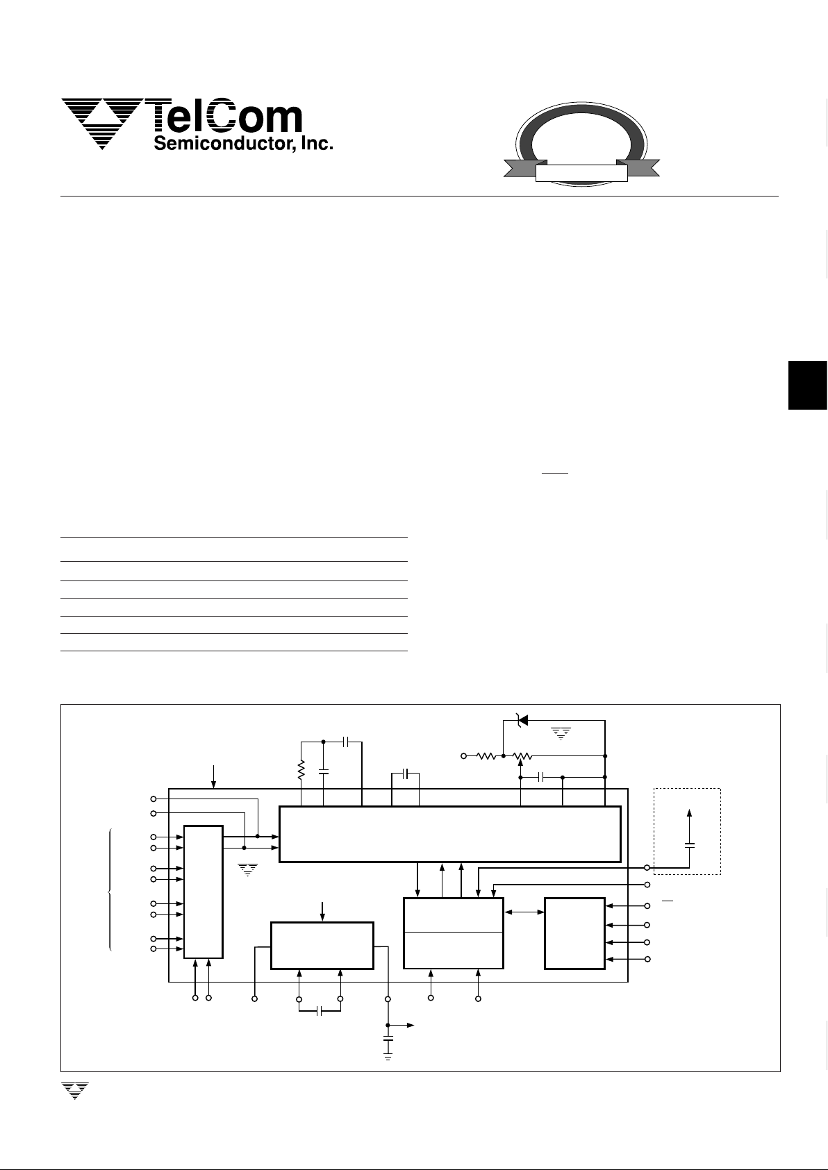
FUNCTIONAL BLOCK DIAGRAM
GENERAL DESCRIPTION
The TC530/534 are serial analog data acquisition subsystems ideal for high precision measurements (up to 17 bits
plus sign). The TC530 consists of a dual slope integrating
A/D converter, negative power supply generator and 3 wire
serial interface port. The TC534 is identical to the TC530, but
adds a four channel differential input multiplexer. Key A/D
converter operating parameters (Auto Zero and Integration
time) are programmable, allowing the user to trade-off
conversion time for resolution.
Data conversion is initiated when the RESET input is
brought low. After conversion, data is loaded into the output
shift register and EOC is asserted indicating new data is
available. The converted data (plus Overrange and polarity
bits) is held in the output shift register until read by the
processor, or until the next conversion is completed allowing
the user to access data at any time.
The TC530/534 timebase can be derived from an external crystal of 2MHz (max), or from an external frequency
source. The TC530/534 requires a single 5V power supply
and features a – 5V, 10mA output which can be used to
supply negative bias to other components in the system.
A0 A1
OSC
IN
EOC
R/W
D
IN
D
OUT
D
CLK
OSC
OUT
OSC
RESET
CAP
+
CAP
–
C
AZ
TC05
TC530
TC534
C
REF
R
INT
C
INT
TC534
(Only)
(TC530 Only)
DC-TO-DC
CONVERTER
State
Machine
Serial Port
Negative
Supply Output
Oscillator
(÷ 4)
Dual Slope A/D Converter
.01µF
0.01µF
Optional
Power-On
Reset Cap
100k
10k
+5V
DIF.
MUX
(TC534
Only)
CH1
CH1
CH2
CH2
CH3
CH3
CH4
CH4
V
IN
VIN
IN
IN
AB
CMPTR
BUF
INT
C
AZ
V
REF
+
V
REF
–
+
C
REF
C
REF
–
ACOM
–
–
–
–
–
+
+
+
+
+
V
DD
V
DD
V
DD
V
DD
V
SS
+
–
3-48
TELCOM SEMICONDUCTOR, INC.
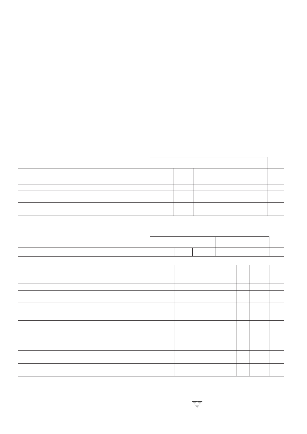
ELECTRICAL CHARACTERISTICS: V
DD
= V
CCD
, CAZ = C
REF
= 0.47µF, unless otherwise specified.
T
A
= +25°C TA = 0°C to +70°C
Symbol Parameter Test Conditions Min Typ Max Min Typ Max Unit
Analog
R Resolution Note 1 — — ±17 — — ±17 Bits
ZSE Zero-Scale Error — — 0.5 — 0.005 0.012 % F.S.
with Auto Zero Phase
ENL End Point Linearity Note 1 and 2 — 0.015 0.030 — 0.015 0.045 % F.S.
NL Max Deviation from Best Notes 1 and 2 — 0.008 0.015 — — — % F.S.
Straight Line Fit
ZS
TC
Zero-Scale Temperature — — — — 1 2 µV/°C
Coefficient
SYE Roll-Over Error Note 3 — .012 — — .03 — % F.S.
FS
TC
Full-Scale Temperature Ext. V
REF
— — — — 10 —
ppm/°C
Coefficient TC = 0ppm/°C
I
IN
Input Current V
IN
= 0V — 6 — — — — pA
V
CMR
Common-Mode V
SS
+ 1.5 — VDD – 1.5
VSS + 1.5
—
V
DD
– 1.5
V
Voltage Range
V
INT
Integrator Output Swing VSS + 0.9 — VDD – 0.9
VSS + 0.9
—
V
DD
– 0.9
V
V
IN
Analog Input Signal Range VSS + 1.5 — VDD – 1.5
VSS + 1.5
—
V
DD
– 1.5
V
V
REF
Voltage Reference Range V
SS
+ 1 — VDD – 1 VDD + 1 —
V
DD
– 1 V
t
D
Zero Crossing Comparator — 2.0 — — 3.0 — µsec
ABSOLUTE MAXIMUM RATINGS*
Supply Voltage ........................................................... +6V
Analog Input Voltage (V
+
IN
or V
–
IN
) ....................... VDD to V
SS
Logic Input Voltage .................(VDD + 0.3V) to (GND – 0.3V)
Ambient Operating Temperature Range
Plastic DIP Package .............................................. (C)
0°C to +70°C
SOIC Package (C)..............................0°C to +70°C
PQFP Package (C)..............................0°C to +70°C
Storage Temperature Range.................... – 65°C to +150°C
Lead Temperature (Soldering, 10 sec) ..................... +300°C
*Stresses beyond those listed under "Absolute Maximum Ratings" may
cause permanent damage to the device. These are stress ratings only, and
functional operation of the device at these or any other conditions beyond
those indicated in the operational sections of the specifications is not
implied. Exposure to absolute maximum rating conditions for extended
periods may affect device reliability.
ELECTRICAL CHARACTERISTICS
T
A
= +25°C TA = 0°C to +70°C
Symbol Parameter Test Conditions Min Typ Max Min Typ Max Unit
V
DD
Analog Power Supply Voltage
4.5 5.0 5.5 4.5 — 5.5 V
V
CCD
Digital Power Supply Voltage
4.5 5.0 5.5 4.5 — 5.5 V
P
D
TC530/534 Total Power VDD = V
CCD
= 5V — — 25 — — — mW
Dissipation
I
S
Supply Current (VS + PIN) — 1.8 2.5 — — 3.0 mA
I
CCD
Supply Current (V
CCD PIN
)f
OSC
= 1MHz — — 1.5 — — 1.7 mA
5V PRECISION DATA ACQUISITION
SUBSYSTEMS
TC530
TC534
3-49
TELCOM SEMICONDUCTOR, INC.
7
6
5
4
3
1
2
8
5V PRECISION DATA ACQUISITION
SUBSYSTEMS
TC530
TC534
ELECTRICAL CHARACTERISTICS:
Serial Port Interface: V
CCD
= +5V, unless otherwise specified.
T
A
= +25°C TA = 0°C to +70°C
Symbol Parameter Test Conditions Min Typ Max Min Typ Max Unit
V
IH
Input Logic HIGH Level 2.5 — — 2.5 — — V
V
IL
Input Logic LOW Level — — 0.8 — — 0.8 V
I
IN
Input Current (DI, DO, D
CLK
) — — 10 ———µA
VOLLogic LOW Output Voltage I
OUT
= 250µA — 0.2 0.3 — — 0.35 V
(EOC)
ELECTRICAL CHARACTERISTICS:
Serial Port Interface: V
CCD
= +5V, unless otherwise specified.
T
A
= +25°C TA = 0°C to +70°C
Symbol Parameter Test Conditions Min Typ Max Min Typ Max Unit
tR, tF Rise and Fall Times CL = 10pF — — 250 — 250 — nsec
(EOC, DI, DO)
F
XTL
Crystal Frequency — — 2.0 — — 2.0 MHz
F
EXT
External Frequency on OSC
IN
— — 4.0 — — 4.0 MHz
t
RS
Read Setup Time 1 — — — 1 — µsec
t
RD
Read Delay Time 250 — — — 250 — nsec
t
DRS
D
CLK
to D
OUT
Delay 450 — — — 450 — nsec
t
PWL
D
CLK
LOW Pulse Width 150 — — — 150 — nsec
t
PWH
D
CLK
HIGH Pulse Width 150 — — — 150 — nsec
t
DR
Data Ready Delay 200 — — — 200 — nsec
ELECTRICAL CHARACTERISTICS:
DC/DC Converter Section: V
DD
= +5V, unless otherwise specified.
T
A
= +25°C TA = 0°C To +70°C
Symbol Parameter Test Conditions Min Typ Max Min Typ Max Unit
R
OUT
Output Resistance I
OUT
= 10mA — 65 85 — — 100 Ω
f
CLK
Oscillator Frequency C
OSC
= 0 — 100 — — — — kHz
I
OUT
VSS Output Current — — 10 — — 10 mA
ELECTRICAL CHARACTERISTICS:
Multiplexer: V
DD
= +5V (Note 4)
, unless otherwise specified.
TA = +25°C TA = 0°C to +70°C
Symbol Parameter Test Conditions Min Typ Max Min Typ Max Unit
V
INMAX
Maximum Input Voltage – 2.5 — 2.5 –2.5 — 2.5 V
R
DS
ON
Drain/Source ON Resistance — 6 10 — — — kΩ
Notes: 1. Integrate time ≥ 66msec, Auto Zero time ≥ 66msec, V
INT
(pk) = 4V.
2. End point linearity at ±¹⁄₄, ±¹⁄₂, ±³⁄₄ F.S. after full scale adjustment.
3. Roll-over error is related to capacitor used for C
INT
(See "Recommended Suppliers for C
INT
", Table 2).
4. TC534 Only.
3-50
TELCOM SEMICONDUCTOR, INC.
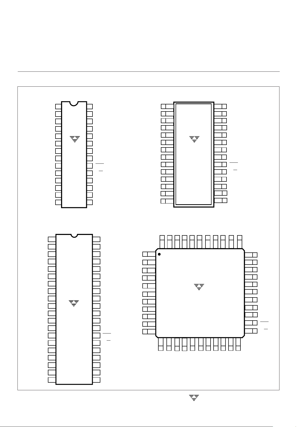
PIN CONFIGURATIONS
1
2
3
4
20
19
18
5
6
7
8
17
23
22
21
9
10
11
12
24
25
26
27
28
TC530CPJ
16
15
13
14
V
V
CCD
D
OUT
D
CLK
C
REF
C
INT
C
AZ
BUF
ACOM
C
REF
REF
V
REF
–
+
–
–
+
CAP
AGND
RESET
–
N/C
EOC
OSC
CAP
+
28
25
24
23
22
21
20
19
18
17
27
26
TC530COI
OSC
OUT
OSC
IN
1
2
3
4
5
6
7
8
9
10
11
12
13
14
1
33
32
31
30
29
28
27
26
25
24
23
2
3
4
5
6
7
8
9
10
11
16
15
V
IN
D
IN
R/W
+
V
IN
DGND
N/C
V
V
SS
V
SS
V
SS
C
REF
C
INT
C
AZ
BUF
ACOM
C
REF
REF
V
REF
–
+
–
–
+
OSC
OUT
V
IN
+
V
IN
DGND
N/C
V
C
REF
C
INT
C
AZ
BUF
ACOM
C
REF
REF
V
REF
–
+
–
+
OSC
OUT
OSC
OUT
DGND
DGND
V
CCD
D
OUT
D
CLK
CAP
AGND
RESET
–
NC
EOC
OSC
CAP
V
CCD
V
CCD
CAP
AGND
AGND
RESET
RESET
OSC
OSC
N/C
N/C
N/C
N/C
N/C
N/C
N/C
N/C
N/C
N/C
+
–
CAP
+
CAP
CAP
–
+
OSC
IN
D
IN
R/W
TC534CPL
1
2
3
4
5
6
7
8
9
10
11
12
13
14
15
16
17
18
19
20
40
39
38
37
36
35
34
33
32
31
30
29
28
27
26
25
24
23
22
21
TC534CKW
A1
A1A0A0
OSC
IN
OSC
IN
D
OUT
D
OUT
D
CLK
D
CLK
EOC
N/C
N/C
N/C
D
IN
D
IN
R/W
R/W
EOC
CH1
+
CH2
+
CH3
+
CH3
+
CH2
+
CH1
+
CH4
+
CH4
–
CH3
–
CH2
–
CH1
–
V
C
REF
ACOM
C
REF
REF
–
+
–
V
REF
+
CH4
+
CH4
–
CH3
–
CH2
–
CH1
–
12 13 14 15
44 43
42
41
39
38
40
N/C
C
INT
37 36 35
34
16
17 18
19 20 21 22
BUF
C
AZ
N/C
N/C
V
DD
V
DD
V
DD
V
SS
V
DD
12 13 14
15
5V PRECISION DATA ACQUISITION
SUBSYSTEMS
TC530
TC534

3-51
TELCOM SEMICONDUCTOR, INC.
7
6
5
4
3
1
2
8
PIN DESCRIPTION
Pin No. Pin No. Pin No Pin No.
(TC530 (TC530 (TC534 (TC534
28-Pin 28-Pin 40-Pin 44-Pin
PDIP, 300 Mil.) SOIC) PDIP) PQFP) Symbol Description
11140VSSAnalog Output. Negative power supply converter output
and reservoir capacitor connection. This output can be
used to provide negative bias to other devices in the system.
22241C
INT
Analog Output. Integrator capacitor connection and integrator
output.
33342CAZAnalog Input. Auto Zero capacitor connection.
4 4 4 43 BUF Analog Output. Integrator capacitor connection and voltage
buffer output.
5 5 5 2 ACOM Analog Input. This pin is ground for all of the analog switches
in the A/D converter. It is grounded for most applications.
ACOM and the input common pin (V
–
IN
or Chx–) should be
within the common mode range, CMR.
6663C
–
REF
Analog Input. Reference cap negative connection.
7774C
+
REF
Analog Input. Reference cap positive connection.
8885V
–
REF
Analog Input. External voltage reference negative connection.
9996V
+
REF
Analog Input. External voltage reference positive connection.
Not Used Not Used 10 7 CH4
–
Analog Input. Multiplexer channel 4 negative differential
analog input.
Not Used Not Used 11 8 CH3
–
Analog Input. Multiplexer channel 3 negative differential
analog input.
Not Used Not Used 12 9 CH2
–
Analog Input. Multiplexer channel 2 negative differential
analog input.
Not Used Not Used 13 10 CH1
–
Analog Input. Multiplexer channel 1 negative differential
analog input.
Not Used Not Used 14 11 CH4
+
Analog Input. Multiplexer channel 4 positive differential
analog input.
Not Used Not Used 15 12 CH3
+
Analog Input. Multiplexer channel 3 positive differential
analog input.
Not Used Not Used 16 13 CH2
+
Analog Input. Multiplexer channel 2 positive differential
analog input.
Not Used Not Used 17 14 CH1
+
Analog Input. Multiplexer channel 1 positive differential
analog input.
10 10 Not Used Not Used V
–
IN
Analog Input. Negative differential analog voltage input.
11 11 Not Used Not Used V
+
IN
Analog Input. Positive differential analog voltage input.
12 12 18 15 DGND Analog Input. Ground connection for serial port circuit.
Not Used Not Used 19 16 A1 Logic Level Input. Multiplexer address MSB.
Not Used Not Used 20 17 A0 Logic Level Input. Multiplexer address LSB.
14 14 21 18 OSC
OUT
Analog Input. Timebase for state machine. This pin connects
to one side of an AT-cut crystal having an effective series
resistance of 100Ω (typ) and a parallel capacitance of 20pF
If an external frequency source is used to clock the TC530/534,
this pin must be left floating.
5V PRECISION DATA ACQUISITION
SUBSYSTEMS
TC530
TC534
 Loading...