

TelCom Semiconductor Inc TC520ACOE, TC520ACPD Datasheet
TC520A
EVALUATION
KIT
AVAILABLE
SERIAL INTERFACE ADAPTER FOR TC500 A/D CONVERTER FAMILY
1
FEATURES
■ Converts TC500/500A/510/514 to Serial Operation
■ Programmable Conversion Rate and Resolution
for Maximum Flexibility
■ Supports up to 17 Bits of Accuracy Plus
Polarity Bit
■ Low Power Operation: Typically 7.5mW
■ 14-Pin DIP or 16-Pin SOIC Packages
■ Polled or Interrupt Mode Operation
ORDERING INFORMATION
Operating
Part No. Package Temp. Range
TC520ACOE 16-Pin SOIC (Wide) 0°C to +70°C
TC520ACPD 14-Pin Plastic DIP 0°C to +70°C
TC500EV Evaluation Kit for TC500 Family
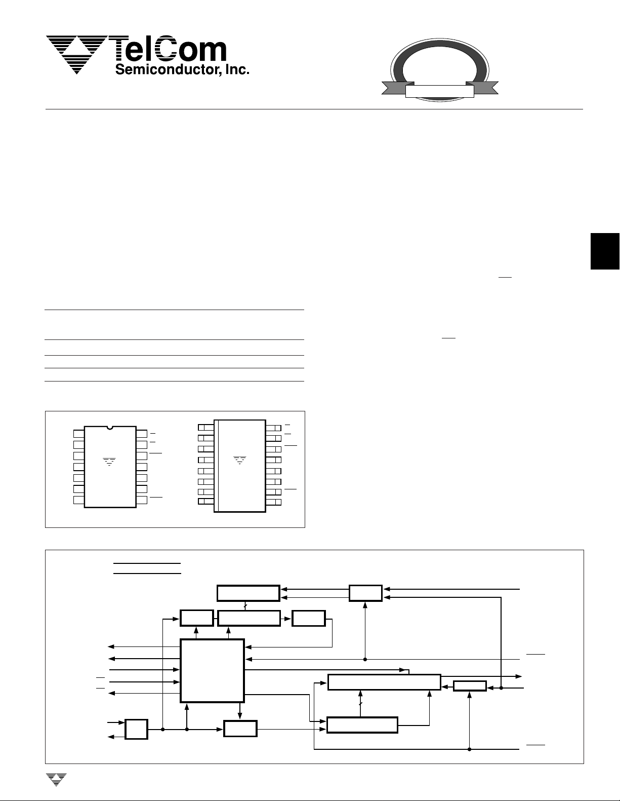
PIN CONFIGURATION
V
V
1
DD
213
DGND
312
CMPTR
411
B
TC520ACPD
510
A
69
OSC
OUT
78
OSC
IN
14
CE
DV
LOAD
D
IN
DCLK
D
OUT
READ
DGND
CMPTR
OSC
OSC
OUT
N/C
1
DD
2
3
4
B
A
IN
5
6
7
8
TC520ACOE
CE
16
DV
15
LOAD
14
D
13
IN
D
12
CLK
D
11
OUT
10
READ
9
N/C
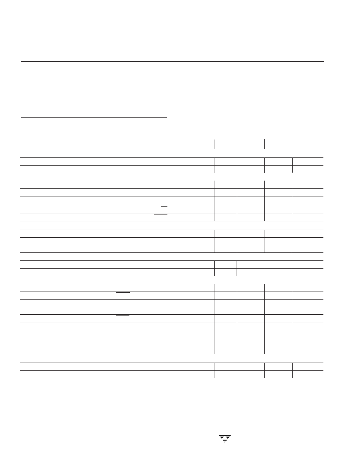
GENERAL DESCRIPTION
The TC520A Serial Interface Adapter provides logic
control for TelCom's TC500/500A/510/514 family of dual
slope, integrating A/D converters. It directly manages TC500
converter phase control signals A, B, and CMPTR thereby
reducing host processor task loading and software complexity. Communication with the TC520A is accomplished over
a 3 wire serial port. Key converter operating parameters are
programmable for complete user flexibility.
Data conversion initiated when the CE input is brought
low. The converted data (plus overrange and polarity bits)
are held in an 18 bit shift register until read by the processor,
or until the next conversion is completed. Data may be
clocked out of the TC520A at any time, and at any rate the
user prefers. A Data Valid (DV) output is driven active at the
start of each conversion cycle indicating the 18 bit shift
register update has just been completed. This signal may be
polled by the processor, or can be used as data ready
interrupt.
The TC520A timebase can be derived from an external
frequency source of up to 6MHz; or can operate from its own
external crystal. It requires a single 5V logic supply and
dissipates less than 7.5mW.
2
3
4
5
FUNCTIONAL BLOCK DIAGRAM
1
V
DD
2
GND
5
A
4
B
CE
DV
OUT
3
14
13
7
IN
÷4
6
CMPTR
OSC
OSC
TELCOM SEMICONDUCTOR, INC.
GATE
LOGIC
CONTROL
SYSCLK
8-BIT SHIFT REG.
8
8-BIT COUNTER
TIME OUT
FORCE AUTO-ZERO
POLARITY BIT
CLEAR COUNT
GATE
÷256
GATE
18-BIT SHIFT REGISTER
16
16-BIT COUNTER
OVERRANGE
BIT
GATE
Pin Out of
14-Pin Package
11
D
IN
12
LOAD
9
D
OUT
10
D
CLK
8
READ
TC520A-1 9/16/96
6
7
8
3-39
TC520A
SERIAL INTERFACE ADAPTER FOR
TC500 A/D CONVERTER FAMILY
ABSOLUTE MAXIMUM RATINGS*
DC Supply Voltage (VDD) ........................................ +6.0V
Input Voltage, All Inputs (VIN)............– 0.3V to VDD +0.3V
Operating Temperature Range (TA).............0°C to +70°C
Storage Temperature Range (T
Lead Temperature (Soldering, 10 sec) (T
ELECTRICAL CHARACTERISTICS: V
) ..... – 65°C to +150°C
STG
) ......+300°C
SDR
DD
= 5V, f
* Static-sensitive device. Unused devices must be stored in conductive
material. Protect devices from static discharge and static fields. Stresses
above those listed under Absolute Maximum Ratings may cause permanent damage to the device. These are stress ratings only and functional
operation of the device at these or any other conditions above those
indicated in the Operational Specifications is not implied. Any exposure to
Absolute Maximum Rating Conditions may affect device reliability.
= 1 MHz, TA = +25°C, unless otherwise specified.
osc
Symbol Parameter Min Typ Max Unit
Supply
V
DD
I
DD
Input Characteristics
V
IL
V
IH
I
IL
I
PD
I
PU
Output Characteristics (I
V
OL
V
OH
tR, t
F
Oscillator (OSCIN, OSC
f
XTL
f
OSC
Timing Characteristics
t
RD
t
RS
t
DRS
t
LS
t
DLS
t
PWL
t
PWH
t
LDL
t
LDS
Parameter
t
IZ
t
AZI
= 250 µA, VDD = 5V)
OUT
)
OUT
Operating Voltage Range 4.5 5 5.5 V
Supply Current — 0.8 1.5 mA
Low Input Voltage — — 0.8 V
High Input Voltage 2.0 — — V
Input Leakage Current — — 10 µA
Pull-down Current (CE) — 5 — µA
Pull-up Current (READ, LOAD) — 5 — µA
Low Output Voltage — 0.2 0.3 V
High Output Voltage 3.5 4.3 — V
CL = 10pF, Rise/Fall Times — — 250 nsec
Crystal Frequency — 1.0 4.0 MHz
External Frequency (OSCIN) — — 6.0 MHz
READ Delay Time 250 — — nsec
Data Read Setup Time 1 — — µsec
D
CLK
to D
Delay 450 — — nsec
OUT
LOAD Setup Time 1 — — µsec
Data Load Setup Time 50 — — nsec
D
Pulse Width Low Time 150 — — nsec
CLK
D
Pulse Width High Time 150 — — nsec
CLK
Load Default Low Time 250 — — nsec
Load Default Setup Time 250 — — nsec
Integrator ZERO Time — 0.5 — msec
Autozero (RESET) Time at Power-Up — 100 — msec
3-40
TELCOM SEMICONDUCTOR, INC.

SERIAL INTERFACE ADAPTER FOR
TC500 A/D CONVERTER FAMILY
DETAILED DESCRIPTION
1
TC520A
The TC520A input and output signals are outlined in the
table below.
PIN DESCRIPTIONS
Pin No. Pin No.
14-Pin PDIP 16-Pin SOIC
Package Package Symbol Description
11VDDInput. +5V ±10% power supply input with respect to DGND.
2 2 DGND Input. Digital Ground.
3 3 CMPTR Input, active high or low (depending on polarity of the voltage input to A/D
converter). This pin connects directly to the zero-crossing comparator output
(CMPTR) of the TC5xx A/D converter. A High-to-Low state change on this pin
causes the TC520A to terminate the de-integrate phase of conversion.
4 4 B Output, active high. The A and B outputs of the TC520A connect directly to the
A and B inputs of the TC5xx A/D converter connected to the TC520A. The
binary code on A, B determines the conversion phase of the TC5xx A/D
converter: (A, B) = 01 places the TC5xx A/D converter into the Auto Zero
phase; (A, B) =10 for Integrate phase (INT); (A, B) =11 for De-integrate phase
(D
) and (A, B) = 00 for Integrator Zero phase (IZ). Please see the TC500
INT
family data sheets for a complete description of these phases of operation.
5 5 A Output, active high. See pin 4 description above.
6 6 OSC
7 7 OSC
8 N/C No connection on 16 pin package version.
9 N/C No connection on 16 pin package version.
8 10 READ Input, active low, level and negative edge triggered. A high-to low transition on
911D
10 12 D
OUT
IN
OUT
CLK
Input. This pin connects to one side of an AT-cut crystal having a effective
series resistance of 100Ω (typ) and a parallel capacitance of 20pF (typ). If an
external frequency source is used to clock the TC520A, this pin must be left
floating.
Input. This pin connects to the other side of the crystal described in pin 6
above. The TC520A may also be clocked from an external frequency source
connected to this pin. The external frequency source must be a pulse train
having a duty cycle of 30% (minimum); rise and fall times of 15nsec and a min/
max amplitude of 0 to V
be left floating. A maximum operating frequency of 4MHz (crystal) or 6MHz
(external clock source) is permitted.
READ loads serial port output shift register with the most recent converted
data. Data is loaded such that the first bit transmitted from the TC520A to the
processor is the overrange bit (OVR), followed by the polarity bit (POL) (high =
input positive; low = input negative). This is followed by a 16 bit data word
(MSB first). (OVR is available at the D
This bit may be used as the 17th data bit if so desired.) The D
serial port is enabled only when READ is held low. Otherwise, D
a high impedance state. A serial port read access cycle is terminated at any
time by bringing READ high.
Output, logic level. Serial port output pin. This pin is enabled only when READ
is low (see READ pin description).
Input, positive and negative edge triggered. Serial port clock. With READ low,
serial data is clocked into the TC520A at each low-to-high transition of D
and clocked out of the TC520A on each high-to-low transition of D
maximum serial port D
. If an external frequency source is used, pin 6 must
IH
as soon as READ is brought low.
OUT
OUT
frequency of 3MHz is permitted.
CLK
pin of the
remains in
OUT
. A
CLK
CLK
2
3
4
5
6
7
,
8
TELCOM SEMICONDUCTOR, INC.
3-41
 Loading...